EP4398037A1 - Composé pour former un film contenant un métal, composition pour former un film contenant un métal, et procédé de formation de motifs - Google Patents
Composé pour former un film contenant un métal, composition pour former un film contenant un métal, et procédé de formation de motifs Download PDFInfo
- Publication number
- EP4398037A1 EP4398037A1 EP23219331.8A EP23219331A EP4398037A1 EP 4398037 A1 EP4398037 A1 EP 4398037A1 EP 23219331 A EP23219331 A EP 23219331A EP 4398037 A1 EP4398037 A1 EP 4398037A1
- Authority
- EP
- European Patent Office
- Prior art keywords
- film
- metal
- pattern
- forming
- resist
- Prior art date
- Legal status (The legal status is an assumption and is not a legal conclusion. Google has not performed a legal analysis and makes no representation as to the accuracy of the status listed.)
- Granted
Links
Images

Classifications
-
- G—PHYSICS
- G03—PHOTOGRAPHY; CINEMATOGRAPHY; ANALOGOUS TECHNIQUES USING WAVES OTHER THAN OPTICAL WAVES; ELECTROGRAPHY; HOLOGRAPHY
- G03F—PHOTOMECHANICAL PRODUCTION OF TEXTURED OR PATTERNED SURFACES, e.g. FOR PRINTING, FOR PROCESSING OF SEMICONDUCTOR DEVICES; MATERIALS THEREFOR; ORIGINALS THEREFOR; APPARATUS SPECIALLY ADAPTED THEREFOR
- G03F7/00—Photomechanical, e.g. photolithographic, production of textured or patterned surfaces, e.g. printing surfaces; Materials therefor, e.g. comprising photoresists; Apparatus specially adapted therefor
- G03F7/004—Photosensitive materials
- G03F7/0042—Photosensitive materials with inorganic or organometallic light-sensitive compounds not otherwise provided for, e.g. inorganic resists
- G03F7/0043—Chalcogenides; Silicon, germanium, arsenic or derivatives thereof; Metals, oxides or alloys thereof
-
- G—PHYSICS
- G03—PHOTOGRAPHY; CINEMATOGRAPHY; ANALOGOUS TECHNIQUES USING WAVES OTHER THAN OPTICAL WAVES; ELECTROGRAPHY; HOLOGRAPHY
- G03F—PHOTOMECHANICAL PRODUCTION OF TEXTURED OR PATTERNED SURFACES, e.g. FOR PRINTING, FOR PROCESSING OF SEMICONDUCTOR DEVICES; MATERIALS THEREFOR; ORIGINALS THEREFOR; APPARATUS SPECIALLY ADAPTED THEREFOR
- G03F7/00—Photomechanical, e.g. photolithographic, production of textured or patterned surfaces, e.g. printing surfaces; Materials therefor, e.g. comprising photoresists; Apparatus specially adapted therefor
- G03F7/004—Photosensitive materials
- G03F7/0042—Photosensitive materials with inorganic or organometallic light-sensitive compounds not otherwise provided for, e.g. inorganic resists
-
- G—PHYSICS
- G03—PHOTOGRAPHY; CINEMATOGRAPHY; ANALOGOUS TECHNIQUES USING WAVES OTHER THAN OPTICAL WAVES; ELECTROGRAPHY; HOLOGRAPHY
- G03F—PHOTOMECHANICAL PRODUCTION OF TEXTURED OR PATTERNED SURFACES, e.g. FOR PRINTING, FOR PROCESSING OF SEMICONDUCTOR DEVICES; MATERIALS THEREFOR; ORIGINALS THEREFOR; APPARATUS SPECIALLY ADAPTED THEREFOR
- G03F7/00—Photomechanical, e.g. photolithographic, production of textured or patterned surfaces, e.g. printing surfaces; Materials therefor, e.g. comprising photoresists; Apparatus specially adapted therefor
- G03F7/004—Photosensitive materials
- G03F7/09—Photosensitive materials characterised by structural details, e.g. supports, auxiliary layers
- G03F7/094—Multilayer resist systems, e.g. planarising layers
-
- C—CHEMISTRY; METALLURGY
- C07—ORGANIC CHEMISTRY
- C07F—ACYCLIC, CARBOCYCLIC OR HETEROCYCLIC COMPOUNDS CONTAINING ELEMENTS OTHER THAN CARBON, HYDROGEN, HALOGEN, OXYGEN, NITROGEN, SULFUR, SELENIUM OR TELLURIUM
- C07F7/00—Compounds containing elements of Groups 4 or 14 of the Periodic Table
- C07F7/22—Tin compounds
- C07F7/2224—Compounds having one or more tin-oxygen linkages
-
- G—PHYSICS
- G03—PHOTOGRAPHY; CINEMATOGRAPHY; ANALOGOUS TECHNIQUES USING WAVES OTHER THAN OPTICAL WAVES; ELECTROGRAPHY; HOLOGRAPHY
- G03F—PHOTOMECHANICAL PRODUCTION OF TEXTURED OR PATTERNED SURFACES, e.g. FOR PRINTING, FOR PROCESSING OF SEMICONDUCTOR DEVICES; MATERIALS THEREFOR; ORIGINALS THEREFOR; APPARATUS SPECIALLY ADAPTED THEREFOR
- G03F1/00—Originals for photomechanical production of textured or patterned surfaces, e.g., masks, photo-masks, reticles; Mask blanks or pellicles therefor; Containers specially adapted therefor; Preparation thereof
- G03F1/68—Preparation processes not covered by groups G03F1/20 - G03F1/50
- G03F1/80—Etching
-
- G—PHYSICS
- G03—PHOTOGRAPHY; CINEMATOGRAPHY; ANALOGOUS TECHNIQUES USING WAVES OTHER THAN OPTICAL WAVES; ELECTROGRAPHY; HOLOGRAPHY
- G03F—PHOTOMECHANICAL PRODUCTION OF TEXTURED OR PATTERNED SURFACES, e.g. FOR PRINTING, FOR PROCESSING OF SEMICONDUCTOR DEVICES; MATERIALS THEREFOR; ORIGINALS THEREFOR; APPARATUS SPECIALLY ADAPTED THEREFOR
- G03F7/00—Photomechanical, e.g. photolithographic, production of textured or patterned surfaces, e.g. printing surfaces; Materials therefor, e.g. comprising photoresists; Apparatus specially adapted therefor
- G03F7/004—Photosensitive materials
- G03F7/0048—Photosensitive materials characterised by the solvents or agents facilitating spreading, e.g. tensio-active agents
-
- G—PHYSICS
- G03—PHOTOGRAPHY; CINEMATOGRAPHY; ANALOGOUS TECHNIQUES USING WAVES OTHER THAN OPTICAL WAVES; ELECTROGRAPHY; HOLOGRAPHY
- G03F—PHOTOMECHANICAL PRODUCTION OF TEXTURED OR PATTERNED SURFACES, e.g. FOR PRINTING, FOR PROCESSING OF SEMICONDUCTOR DEVICES; MATERIALS THEREFOR; ORIGINALS THEREFOR; APPARATUS SPECIALLY ADAPTED THEREFOR
- G03F7/00—Photomechanical, e.g. photolithographic, production of textured or patterned surfaces, e.g. printing surfaces; Materials therefor, e.g. comprising photoresists; Apparatus specially adapted therefor
- G03F7/004—Photosensitive materials
- G03F7/09—Photosensitive materials characterised by structural details, e.g. supports, auxiliary layers
- G03F7/11—Photosensitive materials characterised by structural details, e.g. supports, auxiliary layers having cover layers or intermediate layers, e.g. subbing layers
-
- G—PHYSICS
- G03—PHOTOGRAPHY; CINEMATOGRAPHY; ANALOGOUS TECHNIQUES USING WAVES OTHER THAN OPTICAL WAVES; ELECTROGRAPHY; HOLOGRAPHY
- G03F—PHOTOMECHANICAL PRODUCTION OF TEXTURED OR PATTERNED SURFACES, e.g. FOR PRINTING, FOR PROCESSING OF SEMICONDUCTOR DEVICES; MATERIALS THEREFOR; ORIGINALS THEREFOR; APPARATUS SPECIALLY ADAPTED THEREFOR
- G03F7/00—Photomechanical, e.g. photolithographic, production of textured or patterned surfaces, e.g. printing surfaces; Materials therefor, e.g. comprising photoresists; Apparatus specially adapted therefor
- G03F7/16—Coating processes; Apparatus therefor
- G03F7/161—Coating processes; Apparatus therefor using a previously coated surface, e.g. by stamping or by transfer lamination
-
- G—PHYSICS
- G03—PHOTOGRAPHY; CINEMATOGRAPHY; ANALOGOUS TECHNIQUES USING WAVES OTHER THAN OPTICAL WAVES; ELECTROGRAPHY; HOLOGRAPHY
- G03F—PHOTOMECHANICAL PRODUCTION OF TEXTURED OR PATTERNED SURFACES, e.g. FOR PRINTING, FOR PROCESSING OF SEMICONDUCTOR DEVICES; MATERIALS THEREFOR; ORIGINALS THEREFOR; APPARATUS SPECIALLY ADAPTED THEREFOR
- G03F7/00—Photomechanical, e.g. photolithographic, production of textured or patterned surfaces, e.g. printing surfaces; Materials therefor, e.g. comprising photoresists; Apparatus specially adapted therefor
- G03F7/16—Coating processes; Apparatus therefor
- G03F7/162—Coating on a rotating support, e.g. using a whirler or a spinner
-
- G—PHYSICS
- G03—PHOTOGRAPHY; CINEMATOGRAPHY; ANALOGOUS TECHNIQUES USING WAVES OTHER THAN OPTICAL WAVES; ELECTROGRAPHY; HOLOGRAPHY
- G03F—PHOTOMECHANICAL PRODUCTION OF TEXTURED OR PATTERNED SURFACES, e.g. FOR PRINTING, FOR PROCESSING OF SEMICONDUCTOR DEVICES; MATERIALS THEREFOR; ORIGINALS THEREFOR; APPARATUS SPECIALLY ADAPTED THEREFOR
- G03F7/00—Photomechanical, e.g. photolithographic, production of textured or patterned surfaces, e.g. printing surfaces; Materials therefor, e.g. comprising photoresists; Apparatus specially adapted therefor
- G03F7/16—Coating processes; Apparatus therefor
- G03F7/168—Finishing the coated layer, e.g. drying, baking, soaking
-
- G—PHYSICS
- G03—PHOTOGRAPHY; CINEMATOGRAPHY; ANALOGOUS TECHNIQUES USING WAVES OTHER THAN OPTICAL WAVES; ELECTROGRAPHY; HOLOGRAPHY
- G03F—PHOTOMECHANICAL PRODUCTION OF TEXTURED OR PATTERNED SURFACES, e.g. FOR PRINTING, FOR PROCESSING OF SEMICONDUCTOR DEVICES; MATERIALS THEREFOR; ORIGINALS THEREFOR; APPARATUS SPECIALLY ADAPTED THEREFOR
- G03F7/00—Photomechanical, e.g. photolithographic, production of textured or patterned surfaces, e.g. printing surfaces; Materials therefor, e.g. comprising photoresists; Apparatus specially adapted therefor
- G03F7/20—Exposure; Apparatus therefor
-
- G—PHYSICS
- G03—PHOTOGRAPHY; CINEMATOGRAPHY; ANALOGOUS TECHNIQUES USING WAVES OTHER THAN OPTICAL WAVES; ELECTROGRAPHY; HOLOGRAPHY
- G03F—PHOTOMECHANICAL PRODUCTION OF TEXTURED OR PATTERNED SURFACES, e.g. FOR PRINTING, FOR PROCESSING OF SEMICONDUCTOR DEVICES; MATERIALS THEREFOR; ORIGINALS THEREFOR; APPARATUS SPECIALLY ADAPTED THEREFOR
- G03F7/00—Photomechanical, e.g. photolithographic, production of textured or patterned surfaces, e.g. printing surfaces; Materials therefor, e.g. comprising photoresists; Apparatus specially adapted therefor
- G03F7/26—Processing photosensitive materials; Apparatus therefor
- G03F7/30—Imagewise removal using liquid means
-
- H—ELECTRICITY
- H10—SEMICONDUCTOR DEVICES; ELECTRIC SOLID-STATE DEVICES NOT OTHERWISE PROVIDED FOR
- H10P—GENERIC PROCESSES OR APPARATUS FOR THE MANUFACTURE OR TREATMENT OF DEVICES COVERED BY CLASS H10
- H10P50/00—Etching of wafers, substrates or parts of devices
- H10P50/20—Dry etching; Plasma etching; Reactive-ion etching
- H10P50/28—Dry etching; Plasma etching; Reactive-ion etching of insulating materials
- H10P50/282—Dry etching; Plasma etching; Reactive-ion etching of insulating materials of inorganic materials
- H10P50/283—Dry etching; Plasma etching; Reactive-ion etching of insulating materials of inorganic materials by chemical means
-
- H—ELECTRICITY
- H10—SEMICONDUCTOR DEVICES; ELECTRIC SOLID-STATE DEVICES NOT OTHERWISE PROVIDED FOR
- H10P—GENERIC PROCESSES OR APPARATUS FOR THE MANUFACTURE OR TREATMENT OF DEVICES COVERED BY CLASS H10
- H10P50/00—Etching of wafers, substrates or parts of devices
- H10P50/73—Etching of wafers, substrates or parts of devices using masks for insulating materials
-
- H—ELECTRICITY
- H10—SEMICONDUCTOR DEVICES; ELECTRIC SOLID-STATE DEVICES NOT OTHERWISE PROVIDED FOR
- H10P—GENERIC PROCESSES OR APPARATUS FOR THE MANUFACTURE OR TREATMENT OF DEVICES COVERED BY CLASS H10
- H10P76/00—Manufacture or treatment of masks on semiconductor bodies, e.g. by lithography or photolithography
- H10P76/40—Manufacture or treatment of masks on semiconductor bodies, e.g. by lithography or photolithography of masks comprising inorganic materials
- H10P76/405—Manufacture or treatment of masks on semiconductor bodies, e.g. by lithography or photolithography of masks comprising inorganic materials characterised by their composition, e.g. multilayer masks
-
- H—ELECTRICITY
- H10—SEMICONDUCTOR DEVICES; ELECTRIC SOLID-STATE DEVICES NOT OTHERWISE PROVIDED FOR
- H10P—GENERIC PROCESSES OR APPARATUS FOR THE MANUFACTURE OR TREATMENT OF DEVICES COVERED BY CLASS H10
- H10P76/00—Manufacture or treatment of masks on semiconductor bodies, e.g. by lithography or photolithography
- H10P76/40—Manufacture or treatment of masks on semiconductor bodies, e.g. by lithography or photolithography of masks comprising inorganic materials
- H10P76/408—Manufacture or treatment of masks on semiconductor bodies, e.g. by lithography or photolithography of masks comprising inorganic materials characterised by their sizes, orientations, dispositions, behaviours or shapes
- H10P76/4085—Manufacture or treatment of masks on semiconductor bodies, e.g. by lithography or photolithography of masks comprising inorganic materials characterised by their sizes, orientations, dispositions, behaviours or shapes characterised by the processes involved to create the masks
Definitions
- Patent Document 6 reports that a material containing a Ti compound exhibits excellent dry etching resistance to CHF 3 /CF 4 -based gas and CO 2 /N 2 -based gas.
- An object of the present invention is to provide: a compound for forming a metal-containing film having better dry etching resistance than conventional resist underlayer film materials and also having high filling and planarizing properties; a composition for forming a metal-containing film containing the compound; and a patterning process in which the composition is used.
- the X in the general formula (1) preferably represents an unsaturated hydrocarbon group having 2 to 20 carbon atoms.
- thermosetting property of the compound for forming a metal-containing film can be improved further.
- a compound for forming a metal-containing film having such a structure can achieve high levels of both thermal flowability and thermosetting property.
- this compound is contained in a composition for forming a metal-containing film, it is possible to provide a resist material that exhibits better planarizing and filling properties.
- the compound for forming a metal-containing film preferably satisfies 1.00 ⁇ Mw/Mn ⁇ 1.50, where Mw is a weight-average molecular weight and Mn is a number-average molecular weight measured by gel permeation chromatography in terms of polystyrene.
- a compound for forming a metal-containing film having dispersity of such a range has even better thermal flowability, so that when the compound is contained in a composition for forming a metal-containing film, not only is it possible to fill favorably a fine structure formed on a substrate, it is also possible to form a resist film so that the entire substrate is flat.
- the present invention provides a composition for forming a metal-containing film used in manufacturing a semiconductor, the composition comprising: (A) the above-described compound for forming a metal-containing film; and (B) an organic solvent.
- Such a composition for forming a metal-containing film contains an organotin compound excellent in heat resistance and thermal flowability, and therefore, can provide a resist material having better dry etching resistance than conventional resist underlayer film materials and also having high filling and planarizing properties.
- the composition can further comprise one or more of (C) a crosslinking agent, (E) a surfactant, (F) a flowability accelerator, and (G) an acid generator.
- Such a composition for forming a metal-containing film contains an organotin compound having high levels of both thermal flowability and thermosetting property, and therefore, can provide a resist material that has better dry etching resistance than conventional resist underlayer film materials and also has high filling and planarizing properties.
- the inventive composition for forming a metal-containing film is particularly suitable as a resist underlayer film material.
- the organic solvent (B) may be a mixture of one or more kinds of organic solvent having a boiling point of lower than 180°C and one or more kinds of organic solvent having a boiling point of 180°C or higher ((B1) a high-boiling-point solvent). That is, the organic solvent (B) preferably contains one or more kinds of organic solvent having a boiling point of 180°C or higher as a high-boiling-point solvent (B1).
- the inventive composition for forming a metal-containing film may also contain a crosslinking agent (C).
- the crosslinking agent is not particularly limited, and various known crosslinking agents can be widely used.
- Examples include melamine-based crosslinking agents, acrylate-based crosslinking agents, glycoluril-based crosslinking agents benzoguanamine-based crosslinking agents, urea-based crosslinking agents, ⁇ -hydroxyalkylamide-based crosslinking agents, isocyanurate-based crosslinking agents, aziridine-based crosslinking agents, oxazoline-based crosslinking agents, epoxy-based crosslinking agents, and phenol-based crosslinking agents (e.g. polynuclear phenol-based, such as methylol or alkoxymethyl-based crosslinking agents).
- the crosslinking agent (C) is preferably contained in an amount of 5 to 50 parts by mass, more preferably 10 to 40 parts by mass relative to 100 parts by mass of the compound (A) for forming a metal-containing film.
- acrylate-based crosslinking agents include dipentaerythritol hexaacrylate.
- glycoluril-based crosslinking agents include tetramethoxymethylated glycoluril, tetrabutoxymethylated glycoluril, alkoxy- and/or hydroxy-substituted derivatives thereof, and partial self-condensates thereof.
- ⁇ -hydroxyalkylamide-based crosslinking agent examples include N,N,N',N'-tetra(2-hydroxyethyl)adipic acid amide.
- isocyanurate-based crosslinking agents include triglycidyl isocyanurate and triallyl isocyanurate.
- aziridine-based crosslinking agents include 4,4'-bis(ethyleneiminocarbonylamino)diphenylmethane and 2,2-bishydroxymethylbutanol-tris[3-(1-aziridinyl)propionate].
- oxazoline-based crosslinking agents include 2,2'-isopropylidene bis(4-benzyl-2-oxazoline), 2,2'-isopropylidene bis(4-phenyl-2-oxazoline), 2,2'-methylene bis-4,5-diphenyl-2-oxazoline, 2,2'-methylene bis-4-phenyl-2-oxazoline, 2,2'-methylene bis-4-tert-butyl-2-oxazoline, 2,2'-bis(2-oxazoline), 1,3-phenylene bis(2-oxazoline), 1,4-phenylene bis(2-oxazoline), and a 2-isopropenyloxazoline copolymer.
- epoxy-based crosslinking agents include diglycidyl ether, ethylene glycol diglycidyl ether, 1,4-butanediol diglycidyl ether, 1,4-cyclohexane dimethanol diglycidyl ether, poly(glycidyl methacrylate), trimethylolethane triglycidyl ether, trimethylolpropane triglycidyl ether, and pentaerythritol tetraglycidyl ether.
- polynuclear phenol-based crosslinking agents include compounds represented by the following general formula (XL-1).
- L represents a single bond or a q-valent hydrocarbon group having 1 to 20 carbon atoms
- R 3 represents a hydrogen atom or an alkyl group having 1 to 20 carbon atoms
- q represents an integer of 1 to 5.
- L represents a single bond or a hydrocarbon group having a valency of "q" and having 1 to 20 carbon atoms.
- “q” represents an integer of 1 to 5, more preferably 2 or 3.
- Specific examples of L include groups obtained by removing "q" hydrogen atoms from methane, ethane, propane, butane, isobutane, pentane, cyclopentane, hexane, cyclohexane, methylpentane, methylcyclohexane, dimethylcyclohexane, trimethylcyclohexane, benzene, toluene, xylene, ethylbenzene, ethylisopropylbenzene, diisopropylbenzene, methylnaphthalene, ethylnaphthalene, and eicosane.
- Specific examples of the compounds represented by the general formula (XL-1) include the following compounds. Among these, a hexamethoxymethylated derivative of triphenolmethane, triphenolethane, 1,1,1-tris(4-hydroxyphenyl)ethane, and tris(4-hydroxyphenyl)-1-ethyl-4-isopropylbenzene are preferable from the viewpoint of improving the curability and film thickness uniformity of the metal-containing film.
- R 3 is as defined above.
- a surfactant (E) may be contained in the inventive composition for forming a metal-containing film in order to improve coating property in spin-coating.
- the surfactant include those disclosed in paragraphs [0142] to [0147] of JP2009-269953A .
- the contained amount is preferably 0.01 to 10 parts by mass, more preferably 0.05 to 5 parts by mass per 100 parts by mass of the compound (A) for forming a metal-containing film.
- the flowability accelerator (F) is mixed with the inventive compound for forming a metal-containing film and serves to improve the film-formability by spin-coating and the filling property for a stepped substrate. Furthermore, as the flowability accelerator (F), a material having a high density of carbon atoms and high etching resistance is preferable.
- thermo-decomposable polymer having a weight reduction rate of 40% by mass or more at 30°C to 250°C and a weight-average molecular weight of 300 to 200,000.
- This thermo-decomposable polymer preferably contains a repeating unit having an acetal structure represented by the following general formula (DP1) or (DP1a).
- R 4a represents an alkyl group having 1 to 4 carbon atoms.
- Y a represents a saturated or unsaturated divalent hydrocarbon group having 4 to 10 carbon atoms and optionally having an ether bond.
- "n'" represents an average repeating unit number of 3 to 500.
- One kind of the acid generator can be used, or two or more kinds can be used in combination.
- the contained amount is preferably 0.05 to 50 parts by mass, more preferably 0.1 to 10 parts by mass relative to 100 parts by mass of the compound (A) for forming a metal-containing film.
- the substrate to be processed is coated with the above-described composition for forming a metal-containing film by a spin-coating method or the like.
- a spin-coating method or the like ensures a desirable filling property.
- baking is performed so as to evaporate the solvent and promote a crosslinking reaction to prevent mixing of the resist underlayer film with the resist upper layer film or the resist middle layer film.
- the baking is preferably performed at a temperature of 100°C or higher and 600°C or lower for 10 to 600 seconds, more preferably at a temperature of 200°C or higher and 500°C or lower for 10 to 300 seconds.
- the upper limit of the heating temperature in the wafer process of lithography is preferably not more than 600°C, and more preferably not more than 500°C.
- a substrate to be processed may also be coated with the inventive composition for forming a metal-containing film by spin-coating or the like in the same manner as described above, and then the composition for forming a metal-containing film may be baked and cured under an atmosphere having an oxygen concentration of 0.1 volume % or more and 21 volume % or less to form a metal-containing film as a resist underlayer film.
- the atmosphere during baking may be air; however, to prevent oxidation of the metal-containing film, it is preferable to enclose an inert gas, such as N 2 , Ar, or He, therein to reduce the amount of oxygen. Control of oxygen concentration is necessary to prevent oxidation; the oxygen concentration is preferably 1000 ppm or less, more preferably 100 ppm or less (volumetric basis).
- the method for forming a filling film may be similar to the method for forming a resist underlayer film.
- the present invention provides, as a patterning process according to a two-layer resist process using the above-described composition for forming a metal-containing film, a patterning process for forming a pattern in a substrate to be processed, including the steps of:
- the resist upper layer film in the two-layer resist process described above exhibits etching resistance with respect to chlorine-based gas. Therefore, the dry etching of the metal-containing film that is performed while using the resist upper layer film as a mask in the two-layer resist process is preferably performed using an etching gas mainly containing a chlorine-based gas.
- the present invention provides, as a patterning process according to a three-layer resist process using the above-described composition for forming a metal-containing film, a patterning process for forming a pattern in a substrate to be processed, including the steps of:
- the silicon-containing resist middle layer film in the three-layer resist process exhibits etching resistance with respect to a chlorine-based gas and a hydrogen-based gas. Therefore, the dry etching of the metal-containing film that is performed while using the silicon-containing resist middle layer film as a mask in the three-layer resist process is preferably performed using an etching gas mainly containing a chlorine-based gas or a hydrogen-based gas.
- a polysiloxane-based middle layer film is also preferably used. This allows the silicon-containing resist middle layer film to possess an effect as an antireflective film, thereby suppressing reflection.
- the k-value increases and thus the substrate reflection increases; however, the reflection can be suppressed by imparting absorption so that the silicon-containing resist middle layer film has an appropriate k-value. In this manner, the substrate reflection can be reduced to 0.5% or less.
- the silicon-containing resist middle layer film having an antireflective effect is a polysiloxane, which has a pendant anthracene for exposure at 248 nm or 157 nm, or a pendant phenyl group or a pendant light-absorbing group having a silicon-silicon bond for 193 nm exposure, and which is crosslinked by an acid or heat.
- the present invention provides, as a patterning process by way of a four-layer resist process using such a composition for forming a metal-containing film, a patterning process including the steps of:
- a semiconductor device circuit pattern can be formed on a substrate, at least, by:
- the present invention provides, as a patterning process according to a four-layer resist process using the above-described composition for forming a metal-containing film, a patterning process for forming a pattern in a substrate to be processed, including the steps of:
- a silicon oxide film, a silicon nitride film, and a silicon oxynitride film can be formed by a CVD method, an ALD method, etc.
- the method for forming the silicon nitride film is disclosed, for example, in JP2002-334869A and WO2004/066377A1 .
- the film thickness of the inorganic hard mask middle layer film is preferably 5 to 200 nm, more preferably 10 to 100 nm.
- the SiON film which has a high function as an antireflective film, is the most preferably used as the inorganic hard mask middle layer film.
- the metal-containing film Since the substrate temperature increases to 300 to 500°C when the SiON film is formed, the metal-containing film needs to withstand a temperature of 300 to 500°C.
- the composition for forming a metal-containing film used in the present invention has high heat resistance and can withstand a high temperature of 300 to 500°C.
- the metal-containing film formed by spin-coating and the inorganic hard mask middle layer film formed by the CVD method or the ALD method can be combined.
- a photoresist film may be formed on the inorganic hard mask middle layer film as the resist upper layer film as described above.
- an organic antireflective film (BARC) or an adhesive film may be formed on the inorganic hard mask middle layer film by spin-coating, and a photoresist film may be formed thereon.
- BARC organic antireflective film
- the reflection can be suppressed by the two antireflective films, i.e., the SiON film and the BARC film, even in liquid immersion exposure at a high NA exceeding 1.0.
- Another merit of forming BARC resides in that it has an effect to reduce a footing profile of a photoresist pattern immediately above the SiON film.
- a photoresist film may be formed on the metal-containing film as a resist upper layer film as described above.
- an organic adhesive film may be formed on the metal-containing film by spin-coating, and a photoresist film may be formed thereon.
- the resist underlayer film when the resist underlayer film is formed on the substrate to be processed, the resist underlayer film can be formed by a method using a coating-type resist underlayer film material, a CVD method, an ALD method, or the like.
- the coating-type resist underlayer film material include resins and compositions disclosed in JP2012-001687A , JP2012-077295A , JP2004-264710A , JP2005-043471A , JP2005-250434A , JP2007-293294A , JP2008-065303A , JP2004-205685A , JP2007-171895A , JP2009-014816A , JP2007-199653A , JP2008-274250A , JP2010-122656A , JP2012-214720A , JP2014-029435A , WO2012/077640A1 , WO2010/147155A1 , WO2012/176767A1 , JP2005
- the resist upper layer film in the multilayer resist process described above may be either a positive type or a negative type, and it is possible to use a film similar to the typically used photoresist composition.
- the prebaking which is conducted after the spin-coating with the photoresist composition, is preferably performed at 60 to 180°C for 10 to 300 seconds. Thereafter, exposure is conducted according to a usual manner, followed by post-exposure baking (PEB) and development, thereby obtaining a resist pattern.
- PEB post-exposure baking
- the thickness of the resist upper layer film is not particularly limited, the thickness is preferably 30 to 500 nm, particularly preferably 50 to 400 nm.
- examples of light for exposure include high-energy beams at wavelengths of 300 nm or less, specifically excimer lasers at 248 nm, 193 nm, and 157 nm, soft X-rays at 3 to 20 nm, an electron beam, X-rays, and the like.
- the method for forming a pattern in the resist upper layer film it is preferable to use a patterning process using a photolithography with a wavelength of 5 nm or more and 300 nm or less, a direct drawing using an electron beam, nanoimprinting, or a combination thereof.
- the development method in the patterning process is preferably alkali development or development using an organic solvent.
- the metal-containing film is etched while using the obtained silicon-containing resist middle layer film pattern or inorganic hard mask middle layer film pattern as a mask.
- the etching of the metal-containing film is preferably performed using an etching gas mainly containing a chlorine-based gas.
- the subsequent etching of a body to be processed may also be performed according to a usual manner.
- the etching is performed mainly based on a fluorocarbon-based gas.
- the silicon-containing resist middle layer film pattern in the three-layer resist process is stripped simultaneously with the substrate processing.
- Examples of the body to be processed include, but are not particularly limited to, substrates made of Si, ⁇ -Si, p-Si, SiO 2 , SiN, SiON, W, TiN, Al, etc., those in which the layers to be processed are formed on the substrate, and the like.
- Examples of the layers to be processed include various low-k films such as those made of Si, SiO 2 , SiON, SiN, p-Si, ⁇ -Si, W, W-Si, Al, Cu, Al-Si, and the like, and stopper films therefor, which can each be typically formed into a thickness of 50 to 10,000 nm, particularly 100 to 5,000 nm.
- the substrate and the layer to be processed are made of different materials.
- filling and planarizing by forming a film of the inventive composition for forming a metal-containing film makes it possible to achieve a uniform film thickness in the subsequently formed resist middle layer film and resist upper layer film. Therefore, it is easy to ensure the exposure depth margin (DOF) at the time of photolithography, which is very desirable.
- DOE exposure depth margin
- the present invention provides, as a tone-reversal patterning process using such a composition for forming a metal-containing film, a tone-reversal patterning process for forming a pattern in a substrate to be processed, including the steps of:
- the compound (A-1) for forming a metal-containing film was dissolved at a ratio shown in Table 5 in a mixed solvent of propylene glycol monomethyl ether acetate (PGMEA) and cyclohexanone (CyHO) containing 0.5 mass% of a surfactant FC-4430 (manufactured by Sumitomo 3M Limited), and the solution was filtered through a 0.02- ⁇ m membrane filter to prepare a composition (UDL-1) for forming a metal-containing film.
- PGMEA propylene glycol monomethyl ether acetate
- CyHO cyclohexanone
- Each chemical liquid was prepared in the same manner as UDL-1, except that the type and the contained amount of each component were as shown in Table 5. In Table 5, "-" indicates that the component was not used.
- the following formula (C-1) was used for the crosslinking agent
- the following formula (G-1) was used for the acid generator (TAG)
- 1,6-diacetoxyhexane (boiling point: 260°C) was used as the high-boiling-point solvent (B-1)
- a polymer (F-1) for a flowability accelerator was used as the flowability accelerator.
- the acid generator (G-1) used in a composition for forming a metal-containing film is shown below.
- the organic layer was washed with 100 g of a 3% aqueous nitric acid solution and 100 g of pure water six times, and then the organic layer was dried under reduced pressure to hardness, thereby obtaining a polymer (F-1) for a flowability accelerator.
- the inventive compositions (Examples 1-1 to 1-13) for forming a metal-containing film had a film remaining percentage ((b/a) ⁇ 100) of 45% or more after the additional high-temperature baking, and it was shown that a film that produces little sublimation product can be formed even when compared with Comparative Example 1-3, where a similar composition for forming a metal-containing film was used. Thus, it was shown that the compositions had the high-temperature baking resistance required in resist underlayer films.
- the film remaining percentage ((b/a) ⁇ 100) after the additional high-temperature baking was less than 5%.
- heat resistance was similarly insufficient, and the film remaining after the high-temperature baking was less than 5 nm.
- Comparative Example 1-5 the composition contained, as a compound having a different metal from the inventive compound for forming a metal-containing film, the titanium compound reported in [Synthesis Example A-II] of JP6189758B2 .
- the titanium compound reported in [Synthesis Example A-II] of JP6189758B2 .
- sufficient solvent resistance was exhibited, but the difference between the film thicknesses before and after the additional high-temperature baking was large, and it was shown that volume shrinkage due to high-temperature baking was greater than in the inventive compound for forming a metal-containing film.
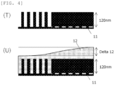
- the substrate used was a base substrate 9 (SiO 2 wafer substrate) having a dense line-and-space pattern shown in FIG. 3(Q) (downward view) and (R) (cross-sectional view).
- Example Composition for forming metal-containing film Baking temperature Flatness °C nm Example 3-1 UDL-1 250°C 33
- Example 3-2 UDL-2 250°C 32
- Example 3-3 UDL-3 250°C 32
- Example 3-4 UDL-4 250°C 31
- Example 3-5 UDL-5 250°C 35
- Example 3-6 UDL-6 250°C 34
- Example 3-7 UDL-7 250°C 31
- Example 3-8 UDL-8 250°C 32
- Example 3-10 UDL-10 250°C 28 Example 3-11 UDL-11 250°C 26
- Example 3-12 UDL-12 250°C 27 Example 3-13 UDL-13 250°C 32
- Comparative Example 3-1 Comparative UDL-3 250°C 31 Comparative Example 3-2 Comparative UDL-5 300°C 57 Comparative Example 3-3 Comparative UDL-6 350°C 49
- Example 3-10 where the used composition (UDL-10) for forming a metal-containing film contained A-10, synthesized by mixing in a different carboxylic acid having a long alkyl chain.
- Examples 3-11 and 3-12 where compositions (UDL-11 and -12) for forming a metal-containing film containing a high-boiling-point solvent (B-1) and a flowability accelerator (F-1) were used, planarizing property was greatly improved compared to Example 3-2, where the additives were not contained.
- B-1 high-boiling-point solvent
- F-1 flowability accelerator
- compositions (UDL-1 to -13 and comparative UDL-3, -5, and -6) for forming a metal-containing film were respectively applied onto a silicon substrate and heated by using a hot plate at the temperature shown in Table 9 for 60 seconds to form a metal-containing film having a film thickness of 100 nm, and the film thickness A was measured.
- etching was performed with CF 4 gas, O 2 gas, and Cl 2 gas under the following conditions for the specified number of seconds by using an etching apparatus CE-300I manufactured by ULVAC, Inc., and the film thickness B was measured.
- the film thickness etched in 1 minute was calculated as etching rate (nm/min) from the film thickness etched in the respective number of seconds ("film thickness B" - "film thickness A").
- Table 9 shows the results.
- compositions (UDL-1 to -13 and comparative UDL-5 and -6) for forming a metal-containing film was respectively applied onto an SiO 2 wafer substrate having a trench pattern (trench width: 10 um, trench depth: 0.10 ⁇ m), and baked at 250°C for 60 seconds in the atmosphere to form a metal-containing film having a thickness of 100 nm.
- a silicon-containing resist middle layer film material (SOG-1) was applied thereto, followed by baking at 220°C for 60 seconds to form a resist middle layer film having a thickness of 30 nm.
- a monolayer resist for ArF as a resist upper layer film material was applied thereto, followed by baking at 105°C for 60 seconds to form a photoresist film having a thickness of 100 nm.
- a liquid immersion top coat composition (TC-1) was applied to the photoresist film, followed by baking at 90°C for 60 seconds to form a top coat having a thickness of 50 nm.
- the silicon-containing resist middle layer film material was prepared by dissolving a polymer represented by an ArF silicon-containing middle layer film polymer (SiP1) and a thermal crosslinking catalyst (CAT1) in an organic solvent containing 0.1 mass% of FC-4430 (manufactured by Sumitomo 3M Limited) in the proportion shown in Table 10; and filtering the solution through a filter made of a fluororesin and having a pore size of 0.1 ⁇ m.
- Polymer Thermal crosslinking catalyst Organic solvent parts by mass
- SOG-1 SiP1 (100)
- CAT1 Propylene glycol monoethyl ether (4, 000)
- the resist upper layer film material (monolayer resist for ArF) was prepared by dissolving a polymer (RP1), an acid generator (PAG1), and a basic compound (Amine1), each in the proportion shown in Table 11, in a solvent containing 0.1% by mass of a surfactant (FC-4430: manufactured by Sumitomo 3M Limited), and filtering the solution through a 0.1-pm filter made of a fluororesin.
- RP1 polymer
- PAG1 acid generator
- Amine1 basic compound
- FC-4430 manufactured by Sumitomo 3M Limited
- the polymer (RP1), the acid generator (PAG1), and the basic compound (Amine1) used for the resist upper layer film material (monolayer resist for ArF) are shown below.
- the liquid immersion top coat composition (TC-1) was prepared by dissolving a top coat polymer (PP1) in an organic solvent at the proportion shown in Table 12, and filtering the solution through a 0.1-pm filter made of a fluororesin.
- Top coat polymer parts by mass
- Organic solvent parts by mass
- TC-1 PP1 100
- Diisoamyl ether (2,700)
- 2-methyl-1-butanol 270
- the top coat polymer (PP1) used for the liquid immersion top coat composition (TC-1) is shown below.
- the substrate was exposed to light with an ArF liquid immersion exposure apparatus (NSR-S610C manufactured by Nikon Corporation, NA: 1.30, ⁇ : 0.98/0.65, 35° s-polarized dipole illumination, 6% halftone phase shift mask), baked at 100°C for 60 seconds (PEB), and developed with a 2.38% by mass aqueous solution of tetramethylammonium hydroxide (TMAH) for 30 seconds, thereby obtaining a 55 nm 1:1 positive line-and-space pattern (a resist upper layer film pattern).
- NSR-S610C ArF liquid immersion exposure apparatus
- NA NA: 1.30
- ⁇ 0.98/0.65, 35° s-polarized dipole illumination, 6% halftone phase shift mask
- the resist middle layer film was etched by dry etching while using the resist upper layer film pattern as a mask to form a hard mask pattern.
- the metal-containing film was then etched while using the obtained hard mask pattern as a mask to form a metal-containing film pattern, and the SiO 2 film was etched while using the obtained metal-containing film pattern as a mask.
- the etching conditions were as follows.
- Table 13 shows the results obtained by observation of the pattern cross section with an electron microscope (S-4700) manufactured by Hitachi, Ltd.
- Example Composition for forming metal-containing film Pattern profile after etching for transferring to substrate Example 5-1 UDL-1 Vertical profile Example 5-2 UDL-2 Vertical profile Example 5-3 UDL-3 Vertical profile Example 5-4 UDL-4 Vertical profile Example 5-5 UDL-5 Vertical profile Example 5-6 UDL-6 Vertical profile Example 5-7 UDL-7 Vertical profile Example 5-8 UDL-8 Vertical profile Example 5-9 UDL-9 Vertical profile Example 5-10 UDL-10 Vertical profile Example 5-11 UDL-11 Vertical profile Example 5-12 UDL-12 Vertical profile Example 5-13 UDL-13 Vertical profile Comparative Example 5-1 Comparative UDL-5 Pattern collapse Comparative Example 5-2 Comparative UDL-6 Distorted pattern
Landscapes
- Physics & Mathematics (AREA)
- General Physics & Mathematics (AREA)
- Chemical & Material Sciences (AREA)
- Organic Chemistry (AREA)
- Engineering & Computer Science (AREA)
- Architecture (AREA)
- Structural Engineering (AREA)
- Metallurgy (AREA)
- Photosensitive Polymer And Photoresist Processing (AREA)
- Materials For Photolithography (AREA)
- Compositions Of Macromolecular Compounds (AREA)
- Polymers With Sulfur, Phosphorus Or Metals In The Main Chain (AREA)
- Exposure Of Semiconductors, Excluding Electron Or Ion Beam Exposure (AREA)
- Organic Low-Molecular-Weight Compounds And Preparation Thereof (AREA)
Applications Claiming Priority (1)
| Application Number | Priority Date | Filing Date | Title |
|---|---|---|---|
| JP2023000802A JP7802711B2 (ja) | 2023-01-06 | 2023-01-06 | 金属含有膜形成用化合物、金属含有膜形成用組成物、及びパターン形成方法 |
Publications (2)
| Publication Number | Publication Date |
|---|---|
| EP4398037A1 true EP4398037A1 (fr) | 2024-07-10 |
| EP4398037B1 EP4398037B1 (fr) | 2026-01-21 |
Family
ID=89308378
Family Applications (1)
| Application Number | Title | Priority Date | Filing Date |
|---|---|---|---|
| EP23219331.8A Active EP4398037B1 (fr) | 2023-01-06 | 2023-12-21 | Composé pour former un film contenant un métal, composition pour former un film contenant un métal, et procédé de formation de motifs |
Country Status (7)
| Country | Link |
|---|---|
| US (1) | US20240402596A1 (fr) |
| EP (1) | EP4398037B1 (fr) |
| JP (1) | JP7802711B2 (fr) |
| KR (1) | KR102910347B1 (fr) |
| CN (1) | CN118307584A (fr) |
| IL (1) | IL309793A (fr) |
| TW (1) | TWI889122B (fr) |
Cited By (1)
| Publication number | Priority date | Publication date | Assignee | Title |
|---|---|---|---|---|
| EP4432011A1 (fr) * | 2023-03-13 | 2024-09-18 | Shin-Etsu Chemical Co., Ltd. | Procédé de formation d'un film de sous-couche de réserve et procédé de formation de motifs |
Families Citing this family (1)
| Publication number | Priority date | Publication date | Assignee | Title |
|---|---|---|---|---|
| KR20250014854A (ko) * | 2023-07-21 | 2025-02-03 | 삼성에스디아이 주식회사 | 반도체 포토레지스트용 조성물 및 이를 이용한 패턴 형성 방법 |
Citations (44)
| Publication number | Priority date | Publication date | Assignee | Title |
|---|---|---|---|---|
| US3053870A (en) * | 1958-05-01 | 1962-09-11 | Union Carbide Corp | Stabilization of resins |
| JP2002334869A (ja) | 2001-02-07 | 2002-11-22 | Tokyo Electron Ltd | シリコン窒化膜の形成方法、形成装置及びこの形成装置の洗浄前処理方法 |
| JP2004205685A (ja) | 2002-12-24 | 2004-07-22 | Shin Etsu Chem Co Ltd | パターン形成方法及び下層膜形成材料 |
| WO2004066377A1 (fr) | 2003-01-24 | 2004-08-05 | Tokyo Electron Limited | Procede de depot chimique en phase vapeur pour former un film de nitrure de silicium sur un substrat |
| JP2004264710A (ja) | 2003-03-04 | 2004-09-24 | Jsr Corp | 反射防止膜形成組成物および反射防止膜 |
| JP2005043471A (ja) | 2003-07-23 | 2005-02-17 | Jsr Corp | 反射防止膜形成組成物及び反射防止膜の形成方法 |
| JP2005128509A (ja) | 2003-10-03 | 2005-05-19 | Shin Etsu Chem Co Ltd | フォトレジスト下層膜形成材料及びパターン形成方法 |
| JP2005250434A (ja) | 2004-02-04 | 2005-09-15 | Shin Etsu Chem Co Ltd | レジスト下層膜材料ならびにパターン形成方法 |
| JP2006227391A (ja) | 2005-02-18 | 2006-08-31 | Shin Etsu Chem Co Ltd | フォトレジスト下層膜形成材料及びパターン形成方法 |
| JP2006259482A (ja) | 2005-03-18 | 2006-09-28 | Shin Etsu Chem Co Ltd | フォトレジスト下層膜形成材料及びパターン形成方法 |
| JP2006259249A (ja) | 2005-03-17 | 2006-09-28 | Shin Etsu Chem Co Ltd | フォトレジスト下層膜形成材料及びパターン形成方法 |
| JP2006285095A (ja) | 2005-04-04 | 2006-10-19 | Shin Etsu Chem Co Ltd | レジスト下層膜材料およびパターン形成方法 |
| JP2006293298A (ja) | 2005-03-11 | 2006-10-26 | Shin Etsu Chem Co Ltd | フォトレジスト下層膜形成材料及びパターン形成方法 |
| JP2007171895A (ja) | 2005-11-28 | 2007-07-05 | Shin Etsu Chem Co Ltd | レジスト下層膜材料及びパターン形成方法 |
| JP2007199653A (ja) | 2005-12-27 | 2007-08-09 | Shin Etsu Chem Co Ltd | フォトレジスト下層膜形成材料及びパターン形成方法 |
| JP2007293294A (ja) | 2006-03-27 | 2007-11-08 | Jsr Corp | 微細パターン形成方法および重合体 |
| JP2007316282A (ja) | 2006-05-25 | 2007-12-06 | Shin Etsu Chem Co Ltd | フォトレジスト下層膜形成材料及びパターン形成方法 |
| JP2008065303A (ja) | 2006-08-10 | 2008-03-21 | Shin Etsu Chem Co Ltd | レジスト下層膜材料及びパターン形成方法 |
| JP2008158002A (ja) | 2006-12-20 | 2008-07-10 | Jsr Corp | レジスト下層膜用組成物及びその製造方法 |
| JP2008274250A (ja) | 2007-04-06 | 2008-11-13 | Osaka Gas Co Ltd | フェノール樹脂およびその製造方法 |
| JP2009014816A (ja) | 2007-07-02 | 2009-01-22 | Jsr Corp | レジスト下層膜形成用組成物及びパターン形成方法 |
| JP2009269953A (ja) | 2008-05-01 | 2009-11-19 | Shin Etsu Chem Co Ltd | 新規光酸発生剤並びにこれを用いたレジスト材料及びパターン形成方法 |
| JP2010122656A (ja) | 2008-10-20 | 2010-06-03 | Shin-Etsu Chemical Co Ltd | レジスト下層膜形成方法、これを用いたパターン形成方法、及びレジスト下層膜材料 |
| WO2010147155A1 (fr) | 2009-06-19 | 2010-12-23 | 日産化学工業株式会社 | Novolaque de carbazole |
| JP2012001687A (ja) | 2010-06-21 | 2012-01-05 | Shin-Etsu Chemical Co Ltd | ナフタレン誘導体、レジスト下層膜材料、レジスト下層膜形成方法及びパターン形成方法 |
| JP2012077295A (ja) | 2010-09-10 | 2012-04-19 | Shin-Etsu Chemical Co Ltd | ナフタレン誘導体及びその製造方法、レジスト下層膜材料、レジスト下層膜形成方法及びパターン形成方法 |
| WO2012077640A1 (fr) | 2010-12-09 | 2012-06-14 | 日産化学工業株式会社 | Composition servant à former une pellicule sous-jacente résistante contenant une résine novolac au carbazole contenant un groupe hydroxyle |
| JP2012145897A (ja) | 2011-01-14 | 2012-08-02 | Shin Etsu Chem Co Ltd | レジスト下層膜材料及びこれを用いたパターン形成方法 |
| JP2012214720A (ja) | 2011-03-28 | 2012-11-08 | Shin-Etsu Chemical Co Ltd | ビフェニル誘導体、レジスト下層膜材料、レジスト下層膜形成方法及びパターン形成方法 |
| WO2012176767A1 (fr) | 2011-06-24 | 2012-12-27 | 日産化学工業株式会社 | Composition formant un film de sous-couche de résist contenant une résine polyhydroxybenzène novolaque |
| JP2014029435A (ja) | 2012-07-31 | 2014-02-13 | Nissan Chem Ind Ltd | カルボニル基含有カルバゾールノボラックを含むリソグラフィー用レジスト下層膜形成組成物 |
| US20150064904A1 (en) * | 2013-08-30 | 2015-03-05 | Az Electronic Materials (Luxembourg) S.A.R.L. | Stable metal compounds as hardmasks and filling materials, their compositions and methods of use |
| JP5708522B2 (ja) | 2011-02-15 | 2015-04-30 | 信越化学工業株式会社 | レジスト材料及びこれを用いたパターン形成方法 |
| JP5708521B2 (ja) | 2011-02-15 | 2015-04-30 | 信越化学工業株式会社 | レジスト材料及びこれを用いたパターン形成方法 |
| US9310684B2 (en) | 2013-08-22 | 2016-04-12 | Inpria Corporation | Organometallic solution based high resolution patterning compositions |
| US20170102612A1 (en) | 2015-10-13 | 2017-04-13 | Inpria Corporation | Organotin oxide hydroxide patterning compositions, precursors, and patterning |
| JP2017119671A (ja) | 2015-12-24 | 2017-07-06 | 信越化学工業株式会社 | 有機膜形成用化合物、有機膜形成用組成物、有機膜形成方法、及びパターン形成方法 |
| JP6189758B2 (ja) | 2013-03-15 | 2017-08-30 | 信越化学工業株式会社 | チタン含有レジスト下層膜形成用組成物及びパターン形成方法 |
| JP2019044022A (ja) | 2017-08-30 | 2019-03-22 | 信越化学工業株式会社 | 有機膜形成用組成物、半導体装置製造用基板、有機膜の形成方法、パターン形成方法、及び重合体 |
| US20190187560A1 (en) * | 2016-05-19 | 2019-06-20 | Mitsui Chemicals, Inc. | Composition for forming metal-containing film, method of producing composition for forming metal-containing film, semiconductor device, and method of producing semiconductor device |
| JP2021162865A (ja) | 2020-04-02 | 2021-10-11 | 三星エスディアイ株式会社Samsung SDI Co., Ltd. | 半導体フォトレジスト用組成物およびこれを利用したパターン形成方法 |
| US20210333708A1 (en) * | 2018-07-31 | 2021-10-28 | Samsung Sdi Co., Ltd. | Semiconductor resist composition, and method of forming patterns using the composition |
| JP2022521531A (ja) | 2019-02-22 | 2022-04-08 | メルク パテント ゲゼルシャフト ミット ベシュレンクテル ハフツング | 改善された貯蔵寿命を有するハードマスク及び充填材料として有用な無機酸化物成分及びアルキニルオキシ置換スピンオン炭素成分を含むスピンオン組成物 |
| KR20220144787A (ko) * | 2018-06-01 | 2022-10-27 | 최상준 | 반사방지용 하드마스크 조성물 |
Family Cites Families (11)
| Publication number | Priority date | Publication date | Assignee | Title |
|---|---|---|---|---|
| JP6372887B2 (ja) * | 2015-05-14 | 2018-08-15 | 信越化学工業株式会社 | 有機膜材料、有機膜形成方法、パターン形成方法、及び化合物 |
| KR102918243B1 (ko) * | 2017-11-20 | 2026-01-26 | 인프리아 코포레이션 | 유기주석 클러스터, 유기주석 클러스터의 용액, 및 고해상도 패턴화에 대한 적용 |
| JP7145143B2 (ja) * | 2019-12-12 | 2022-09-30 | 信越化学工業株式会社 | 有機膜形成材料、有機膜の形成方法、パターン形成方法、および化合物 |
| JP7285209B2 (ja) * | 2019-12-26 | 2023-06-01 | 信越化学工業株式会社 | 下層膜形成材料、下層膜の形成方法、及びパターン形成方法 |
| JP7368322B2 (ja) * | 2020-06-12 | 2023-10-24 | 信越化学工業株式会社 | レジスト下層膜材料、パターン形成方法、及びレジスト下層膜形成方法 |
| JP2023535894A (ja) * | 2020-07-17 | 2023-08-22 | ラム リサーチ コーポレーション | Sn(ii)前駆体からのフォトレジスト |
| JPWO2022102636A1 (fr) * | 2020-11-12 | 2022-05-19 | ||
| JP7445583B2 (ja) * | 2020-11-25 | 2024-03-07 | 信越化学工業株式会社 | レジスト下層膜材料、パターン形成方法、及びレジスト下層膜形成方法 |
| KR102690557B1 (ko) * | 2020-12-18 | 2024-07-30 | 삼성에스디아이 주식회사 | 반도체 포토레지스트용 조성물, 이의 제조 방법 및 이를 이용한 패턴 형성 방법 |
| US12265332B2 (en) * | 2021-06-18 | 2025-04-01 | Taiwan Semiconductor Manufacturing Company, Ltd. | Method of manufacturing a semiconductor device |
| JP2024041705A (ja) * | 2022-09-14 | 2024-03-27 | 信越化学工業株式会社 | 金属含有膜形成用化合物、金属含有膜形成用組成物、パターン形成方法、及び半導体フォトレジスト材料 |
-
2023
- 2023-01-06 JP JP2023000802A patent/JP7802711B2/ja active Active
- 2023-12-21 EP EP23219331.8A patent/EP4398037B1/fr active Active
- 2023-12-27 IL IL309793A patent/IL309793A/en unknown
-
2024
- 2024-01-02 US US18/402,520 patent/US20240402596A1/en active Pending
- 2024-01-03 KR KR1020240000954A patent/KR102910347B1/ko active Active
- 2024-01-03 TW TW113100172A patent/TWI889122B/zh active
- 2024-01-03 CN CN202410005941.8A patent/CN118307584A/zh active Pending
Patent Citations (45)
| Publication number | Priority date | Publication date | Assignee | Title |
|---|---|---|---|---|
| US3053870A (en) * | 1958-05-01 | 1962-09-11 | Union Carbide Corp | Stabilization of resins |
| JP2002334869A (ja) | 2001-02-07 | 2002-11-22 | Tokyo Electron Ltd | シリコン窒化膜の形成方法、形成装置及びこの形成装置の洗浄前処理方法 |
| JP2004205685A (ja) | 2002-12-24 | 2004-07-22 | Shin Etsu Chem Co Ltd | パターン形成方法及び下層膜形成材料 |
| WO2004066377A1 (fr) | 2003-01-24 | 2004-08-05 | Tokyo Electron Limited | Procede de depot chimique en phase vapeur pour former un film de nitrure de silicium sur un substrat |
| JP2004264710A (ja) | 2003-03-04 | 2004-09-24 | Jsr Corp | 反射防止膜形成組成物および反射防止膜 |
| JP2005043471A (ja) | 2003-07-23 | 2005-02-17 | Jsr Corp | 反射防止膜形成組成物及び反射防止膜の形成方法 |
| JP2005128509A (ja) | 2003-10-03 | 2005-05-19 | Shin Etsu Chem Co Ltd | フォトレジスト下層膜形成材料及びパターン形成方法 |
| JP2005250434A (ja) | 2004-02-04 | 2005-09-15 | Shin Etsu Chem Co Ltd | レジスト下層膜材料ならびにパターン形成方法 |
| JP2006227391A (ja) | 2005-02-18 | 2006-08-31 | Shin Etsu Chem Co Ltd | フォトレジスト下層膜形成材料及びパターン形成方法 |
| JP2006293298A (ja) | 2005-03-11 | 2006-10-26 | Shin Etsu Chem Co Ltd | フォトレジスト下層膜形成材料及びパターン形成方法 |
| JP2006259249A (ja) | 2005-03-17 | 2006-09-28 | Shin Etsu Chem Co Ltd | フォトレジスト下層膜形成材料及びパターン形成方法 |
| JP2006259482A (ja) | 2005-03-18 | 2006-09-28 | Shin Etsu Chem Co Ltd | フォトレジスト下層膜形成材料及びパターン形成方法 |
| JP2006285095A (ja) | 2005-04-04 | 2006-10-19 | Shin Etsu Chem Co Ltd | レジスト下層膜材料およびパターン形成方法 |
| JP2007171895A (ja) | 2005-11-28 | 2007-07-05 | Shin Etsu Chem Co Ltd | レジスト下層膜材料及びパターン形成方法 |
| JP2007199653A (ja) | 2005-12-27 | 2007-08-09 | Shin Etsu Chem Co Ltd | フォトレジスト下層膜形成材料及びパターン形成方法 |
| JP2007293294A (ja) | 2006-03-27 | 2007-11-08 | Jsr Corp | 微細パターン形成方法および重合体 |
| JP2007316282A (ja) | 2006-05-25 | 2007-12-06 | Shin Etsu Chem Co Ltd | フォトレジスト下層膜形成材料及びパターン形成方法 |
| JP2008065303A (ja) | 2006-08-10 | 2008-03-21 | Shin Etsu Chem Co Ltd | レジスト下層膜材料及びパターン形成方法 |
| JP2008158002A (ja) | 2006-12-20 | 2008-07-10 | Jsr Corp | レジスト下層膜用組成物及びその製造方法 |
| JP2008274250A (ja) | 2007-04-06 | 2008-11-13 | Osaka Gas Co Ltd | フェノール樹脂およびその製造方法 |
| JP2009014816A (ja) | 2007-07-02 | 2009-01-22 | Jsr Corp | レジスト下層膜形成用組成物及びパターン形成方法 |
| JP2009269953A (ja) | 2008-05-01 | 2009-11-19 | Shin Etsu Chem Co Ltd | 新規光酸発生剤並びにこれを用いたレジスト材料及びパターン形成方法 |
| JP2010122656A (ja) | 2008-10-20 | 2010-06-03 | Shin-Etsu Chemical Co Ltd | レジスト下層膜形成方法、これを用いたパターン形成方法、及びレジスト下層膜材料 |
| WO2010147155A1 (fr) | 2009-06-19 | 2010-12-23 | 日産化学工業株式会社 | Novolaque de carbazole |
| JP2012001687A (ja) | 2010-06-21 | 2012-01-05 | Shin-Etsu Chemical Co Ltd | ナフタレン誘導体、レジスト下層膜材料、レジスト下層膜形成方法及びパターン形成方法 |
| JP2012077295A (ja) | 2010-09-10 | 2012-04-19 | Shin-Etsu Chemical Co Ltd | ナフタレン誘導体及びその製造方法、レジスト下層膜材料、レジスト下層膜形成方法及びパターン形成方法 |
| WO2012077640A1 (fr) | 2010-12-09 | 2012-06-14 | 日産化学工業株式会社 | Composition servant à former une pellicule sous-jacente résistante contenant une résine novolac au carbazole contenant un groupe hydroxyle |
| JP2012145897A (ja) | 2011-01-14 | 2012-08-02 | Shin Etsu Chem Co Ltd | レジスト下層膜材料及びこれを用いたパターン形成方法 |
| JP5708522B2 (ja) | 2011-02-15 | 2015-04-30 | 信越化学工業株式会社 | レジスト材料及びこれを用いたパターン形成方法 |
| JP5708521B2 (ja) | 2011-02-15 | 2015-04-30 | 信越化学工業株式会社 | レジスト材料及びこれを用いたパターン形成方法 |
| JP2012214720A (ja) | 2011-03-28 | 2012-11-08 | Shin-Etsu Chemical Co Ltd | ビフェニル誘導体、レジスト下層膜材料、レジスト下層膜形成方法及びパターン形成方法 |
| WO2012176767A1 (fr) | 2011-06-24 | 2012-12-27 | 日産化学工業株式会社 | Composition formant un film de sous-couche de résist contenant une résine polyhydroxybenzène novolaque |
| JP2014029435A (ja) | 2012-07-31 | 2014-02-13 | Nissan Chem Ind Ltd | カルボニル基含有カルバゾールノボラックを含むリソグラフィー用レジスト下層膜形成組成物 |
| JP6189758B2 (ja) | 2013-03-15 | 2017-08-30 | 信越化学工業株式会社 | チタン含有レジスト下層膜形成用組成物及びパターン形成方法 |
| US9310684B2 (en) | 2013-08-22 | 2016-04-12 | Inpria Corporation | Organometallic solution based high resolution patterning compositions |
| US20150064904A1 (en) * | 2013-08-30 | 2015-03-05 | Az Electronic Materials (Luxembourg) S.A.R.L. | Stable metal compounds as hardmasks and filling materials, their compositions and methods of use |
| JP7050137B2 (ja) | 2013-08-30 | 2022-04-07 | メルク パテント ゲゼルシャフト ミット ベシュレンクテル ハフツング | ハードマスクおよび充填材料として安定な金属化合物、その組成物、およびその使用方法 |
| US20170102612A1 (en) | 2015-10-13 | 2017-04-13 | Inpria Corporation | Organotin oxide hydroxide patterning compositions, precursors, and patterning |
| JP2017119671A (ja) | 2015-12-24 | 2017-07-06 | 信越化学工業株式会社 | 有機膜形成用化合物、有機膜形成用組成物、有機膜形成方法、及びパターン形成方法 |
| US20190187560A1 (en) * | 2016-05-19 | 2019-06-20 | Mitsui Chemicals, Inc. | Composition for forming metal-containing film, method of producing composition for forming metal-containing film, semiconductor device, and method of producing semiconductor device |
| JP2019044022A (ja) | 2017-08-30 | 2019-03-22 | 信越化学工業株式会社 | 有機膜形成用組成物、半導体装置製造用基板、有機膜の形成方法、パターン形成方法、及び重合体 |
| KR20220144787A (ko) * | 2018-06-01 | 2022-10-27 | 최상준 | 반사방지용 하드마스크 조성물 |
| US20210333708A1 (en) * | 2018-07-31 | 2021-10-28 | Samsung Sdi Co., Ltd. | Semiconductor resist composition, and method of forming patterns using the composition |
| JP2022521531A (ja) | 2019-02-22 | 2022-04-08 | メルク パテント ゲゼルシャフト ミット ベシュレンクテル ハフツング | 改善された貯蔵寿命を有するハードマスク及び充填材料として有用な無機酸化物成分及びアルキニルオキシ置換スピンオン炭素成分を含むスピンオン組成物 |
| JP2021162865A (ja) | 2020-04-02 | 2021-10-11 | 三星エスディアイ株式会社Samsung SDI Co., Ltd. | 半導体フォトレジスト用組成物およびこれを利用したパターン形成方法 |
Cited By (2)
| Publication number | Priority date | Publication date | Assignee | Title |
|---|---|---|---|---|
| EP4432011A1 (fr) * | 2023-03-13 | 2024-09-18 | Shin-Etsu Chemical Co., Ltd. | Procédé de formation d'un film de sous-couche de réserve et procédé de formation de motifs |
| KR20240139010A (ko) * | 2023-03-13 | 2024-09-20 | 신에쓰 가가꾸 고교 가부시끼가이샤 | 레지스트 하층막 형성 방법, 패턴 형성 방법 |
Also Published As
| Publication number | Publication date |
|---|---|
| TW202437014A (zh) | 2024-09-16 |
| KR102910347B1 (ko) | 2026-01-08 |
| EP4398037B1 (fr) | 2026-01-21 |
| JP7802711B2 (ja) | 2026-01-20 |
| JP2024097389A (ja) | 2024-07-19 |
| IL309793A (en) | 2024-08-01 |
| CN118307584A (zh) | 2024-07-09 |
| KR20240110503A (ko) | 2024-07-15 |
| US20240402596A1 (en) | 2024-12-05 |
| TWI889122B (zh) | 2025-07-01 |
Similar Documents
| Publication | Publication Date | Title |
|---|---|---|
| EP4369100A1 (fr) | Composé pour former un film contenant un métal, composition pour former un film contenant un métal, et procédé de formation de motifs | |
| EP4239409A1 (fr) | Composition pour former un film d'oxyde métallique, procédé de formation de motifs et procédé de formation d'un film d'oxyde métallique | |
| EP4398037B1 (fr) | Composé pour former un film contenant un métal, composition pour former un film contenant un métal, et procédé de formation de motifs | |
| EP4390547A1 (fr) | Polymère pour former un film contenant un métal, composition pour former un film contenant un métal, et procédé de formation de motifs | |
| EP4339702A1 (fr) | Composé pour former un film contenant un métal, composition pour former un film contenant un métal, procédé de formation de motifs et matériau de résine photosensible semi-conductrice | |
| EP4398036A1 (fr) | Composé pour former un film contenant un métal, composition pour former un film contenant un métal, et procédé de formation de motifs | |
| EP4239408A1 (fr) | Composition pour former un film organique, procédé de formation de motifs et composé | |
| JP2024041705A (ja) | 金属含有膜形成用化合物、金属含有膜形成用組成物、パターン形成方法、及び半導体フォトレジスト材料 | |
| EP4524656A1 (fr) | Composé pour former un film contenant un métal, composition pour former un film contenant un métal, et procédé de formation de motifs | |
| EP4517426A2 (fr) | Composé pour former un film contenant un métal, composition pour former un film contenant un métal, et procédé de formation de motifs | |
| EP4418044A1 (fr) | Composé pour former un film contenant un métal, composition pour former un film contenant un métal, et procédé de formation de motifs | |
| EP4575640A2 (fr) | Composé pour former un film contenant un métal, composition pour former un film contenant un métal, et procédé de formation de motifs | |
| EP4390548A1 (fr) | Composé pour former un film contenant un métal, composition pour former un film contenant un métal, et procédé de formation de motifs | |
| EP4575641A2 (fr) | Composé pour former un film contenant un métal, composition pour former un film contenant un métal, et procédé de formation de motifs | |
| CN117700444A (zh) | 含金属的膜形成用化合物和组成物、图案形成方法及半导体光致抗蚀剂材料 |
Legal Events
| Date | Code | Title | Description |
|---|---|---|---|
| PUAI | Public reference made under article 153(3) epc to a published international application that has entered the european phase |
Free format text: ORIGINAL CODE: 0009012 |
|
| STAA | Information on the status of an ep patent application or granted ep patent |
Free format text: STATUS: THE APPLICATION HAS BEEN PUBLISHED |
|
| AK | Designated contracting states |
Kind code of ref document: A1 Designated state(s): AL AT BE BG CH CY CZ DE DK EE ES FI FR GB GR HR HU IE IS IT LI LT LU LV MC ME MK MT NL NO PL PT RO RS SE SI SK SM TR |
|
| STAA | Information on the status of an ep patent application or granted ep patent |
Free format text: STATUS: REQUEST FOR EXAMINATION WAS MADE |
|
| 17P | Request for examination filed |
Effective date: 20240812 |
|
| RBV | Designated contracting states (corrected) |
Designated state(s): AL AT BE BG CH CY CZ DE DK EE ES FI FR GB GR HR HU IE IS IT LI LT LU LV MC ME MK MT NL NO PL PT RO RS SE SI SK SM TR |
|
| GRAP | Despatch of communication of intention to grant a patent |
Free format text: ORIGINAL CODE: EPIDOSNIGR1 |
|
| STAA | Information on the status of an ep patent application or granted ep patent |
Free format text: STATUS: GRANT OF PATENT IS INTENDED |
|
| RIC1 | Information provided on ipc code assigned before grant |
Ipc: G03F 7/09 20060101AFI20250912BHEP Ipc: C07F 7/22 20060101ALI20250912BHEP Ipc: H01L 21/027 20060101ALI20250912BHEP Ipc: H01L 21/033 20060101ALI20250912BHEP |
|
| INTG | Intention to grant announced |
Effective date: 20251016 |
|
| GRAS | Grant fee paid |
Free format text: ORIGINAL CODE: EPIDOSNIGR3 |
|
| GRAA | (expected) grant |
Free format text: ORIGINAL CODE: 0009210 |
|
| STAA | Information on the status of an ep patent application or granted ep patent |
Free format text: STATUS: THE PATENT HAS BEEN GRANTED |
|
| AK | Designated contracting states |
Kind code of ref document: B1 Designated state(s): AL AT BE BG CH CY CZ DE DK EE ES FI FR GB GR HR HU IE IS IT LI LT LU LV MC ME MK MT NL NO PL PT RO RS SE SI SK SM TR |
|
| REG | Reference to a national code |
Ref country code: CH Ref legal event code: F10 Free format text: ST27 STATUS EVENT CODE: U-0-0-F10-F00 (AS PROVIDED BY THE NATIONAL OFFICE) Effective date: 20260121 |
|
| REG | Reference to a national code |
Ref country code: DE Ref legal event code: R096 Ref document number: 602023010990 Country of ref document: DE |
|
| REG | Reference to a national code |
Ref country code: IE Ref legal event code: FG4D |