EP4398315A2 - Solarzellen mit verbesserter lebensdauer, passivierung und/oder effizienz - Google Patents
Solarzellen mit verbesserter lebensdauer, passivierung und/oder effizienz Download PDFInfo
- Publication number
- EP4398315A2 EP4398315A2 EP24176520.5A EP24176520A EP4398315A2 EP 4398315 A2 EP4398315 A2 EP 4398315A2 EP 24176520 A EP24176520 A EP 24176520A EP 4398315 A2 EP4398315 A2 EP 4398315A2
- Authority
- EP
- European Patent Office
- Prior art keywords
- solar cell
- region
- silicon substrate
- emitter region
- formed over
- Prior art date
- Legal status (The legal status is an assumption and is not a legal conclusion. Google has not performed a legal analysis and makes no representation as to the accuracy of the status listed.)
- Pending
Links
Images




Classifications
-
- H—ELECTRICITY
- H10—SEMICONDUCTOR DEVICES; ELECTRIC SOLID-STATE DEVICES NOT OTHERWISE PROVIDED FOR
- H10F—INORGANIC SEMICONDUCTOR DEVICES SENSITIVE TO INFRARED RADIATION, LIGHT, ELECTROMAGNETIC RADIATION OF SHORTER WAVELENGTH OR CORPUSCULAR RADIATION
- H10F77/00—Constructional details of devices covered by this subclass
- H10F77/93—Interconnections
- H10F77/933—Interconnections for devices having potential barriers
- H10F77/935—Interconnections for devices having potential barriers for photovoltaic devices or modules
-
- H—ELECTRICITY
- H10—SEMICONDUCTOR DEVICES; ELECTRIC SOLID-STATE DEVICES NOT OTHERWISE PROVIDED FOR
- H10F—INORGANIC SEMICONDUCTOR DEVICES SENSITIVE TO INFRARED RADIATION, LIGHT, ELECTROMAGNETIC RADIATION OF SHORTER WAVELENGTH OR CORPUSCULAR RADIATION
- H10F10/00—Individual photovoltaic cells, e.g. solar cells
- H10F10/10—Individual photovoltaic cells, e.g. solar cells having potential barriers
- H10F10/14—Photovoltaic cells having only PN homojunction potential barriers
- H10F10/148—Double-emitter photovoltaic cells, e.g. bifacial photovoltaic cells
-
- H—ELECTRICITY
- H10—SEMICONDUCTOR DEVICES; ELECTRIC SOLID-STATE DEVICES NOT OTHERWISE PROVIDED FOR
- H10F—INORGANIC SEMICONDUCTOR DEVICES SENSITIVE TO INFRARED RADIATION, LIGHT, ELECTROMAGNETIC RADIATION OF SHORTER WAVELENGTH OR CORPUSCULAR RADIATION
- H10F77/00—Constructional details of devices covered by this subclass
- H10F77/20—Electrodes
- H10F77/206—Electrodes for devices having potential barriers
- H10F77/211—Electrodes for devices having potential barriers for photovoltaic cells
-
- H—ELECTRICITY
- H10—SEMICONDUCTOR DEVICES; ELECTRIC SOLID-STATE DEVICES NOT OTHERWISE PROVIDED FOR
- H10F—INORGANIC SEMICONDUCTOR DEVICES SENSITIVE TO INFRARED RADIATION, LIGHT, ELECTROMAGNETIC RADIATION OF SHORTER WAVELENGTH OR CORPUSCULAR RADIATION
- H10F10/00—Individual photovoltaic cells, e.g. solar cells
- H10F10/10—Individual photovoltaic cells, e.g. solar cells having potential barriers
- H10F10/14—Photovoltaic cells having only PN homojunction potential barriers
-
- H—ELECTRICITY
- H10—SEMICONDUCTOR DEVICES; ELECTRIC SOLID-STATE DEVICES NOT OTHERWISE PROVIDED FOR
- H10F—INORGANIC SEMICONDUCTOR DEVICES SENSITIVE TO INFRARED RADIATION, LIGHT, ELECTROMAGNETIC RADIATION OF SHORTER WAVELENGTH OR CORPUSCULAR RADIATION
- H10F10/00—Individual photovoltaic cells, e.g. solar cells
- H10F10/10—Individual photovoltaic cells, e.g. solar cells having potential barriers
- H10F10/14—Photovoltaic cells having only PN homojunction potential barriers
- H10F10/146—Back-junction photovoltaic cells, e.g. having interdigitated base-emitter regions on the back side
-
- H—ELECTRICITY
- H10—SEMICONDUCTOR DEVICES; ELECTRIC SOLID-STATE DEVICES NOT OTHERWISE PROVIDED FOR
- H10F—INORGANIC SEMICONDUCTOR DEVICES SENSITIVE TO INFRARED RADIATION, LIGHT, ELECTROMAGNETIC RADIATION OF SHORTER WAVELENGTH OR CORPUSCULAR RADIATION
- H10F10/00—Individual photovoltaic cells, e.g. solar cells
- H10F10/10—Individual photovoltaic cells, e.g. solar cells having potential barriers
- H10F10/16—Photovoltaic cells having only PN heterojunction potential barriers
- H10F10/164—Photovoltaic cells having only PN heterojunction potential barriers comprising heterojunctions with Group IV materials, e.g. ITO/Si or GaAs/SiGe photovoltaic cells
- H10F10/165—Photovoltaic cells having only PN heterojunction potential barriers comprising heterojunctions with Group IV materials, e.g. ITO/Si or GaAs/SiGe photovoltaic cells the heterojunctions being Group IV-IV heterojunctions, e.g. Si/Ge, SiGe/Si or Si/SiC photovoltaic cells
-
- H—ELECTRICITY
- H10—SEMICONDUCTOR DEVICES; ELECTRIC SOLID-STATE DEVICES NOT OTHERWISE PROVIDED FOR
- H10F—INORGANIC SEMICONDUCTOR DEVICES SENSITIVE TO INFRARED RADIATION, LIGHT, ELECTROMAGNETIC RADIATION OF SHORTER WAVELENGTH OR CORPUSCULAR RADIATION
- H10F10/00—Individual photovoltaic cells, e.g. solar cells
- H10F10/10—Individual photovoltaic cells, e.g. solar cells having potential barriers
- H10F10/16—Photovoltaic cells having only PN heterojunction potential barriers
- H10F10/164—Photovoltaic cells having only PN heterojunction potential barriers comprising heterojunctions with Group IV materials, e.g. ITO/Si or GaAs/SiGe photovoltaic cells
- H10F10/165—Photovoltaic cells having only PN heterojunction potential barriers comprising heterojunctions with Group IV materials, e.g. ITO/Si or GaAs/SiGe photovoltaic cells the heterojunctions being Group IV-IV heterojunctions, e.g. Si/Ge, SiGe/Si or Si/SiC photovoltaic cells
- H10F10/166—Photovoltaic cells having only PN heterojunction potential barriers comprising heterojunctions with Group IV materials, e.g. ITO/Si or GaAs/SiGe photovoltaic cells the heterojunctions being Group IV-IV heterojunctions, e.g. Si/Ge, SiGe/Si or Si/SiC photovoltaic cells the Group IV-IV heterojunctions being heterojunctions of crystalline and amorphous materials, e.g. silicon heterojunction [SHJ] photovoltaic cells
-
- H—ELECTRICITY
- H10—SEMICONDUCTOR DEVICES; ELECTRIC SOLID-STATE DEVICES NOT OTHERWISE PROVIDED FOR
- H10F—INORGANIC SEMICONDUCTOR DEVICES SENSITIVE TO INFRARED RADIATION, LIGHT, ELECTROMAGNETIC RADIATION OF SHORTER WAVELENGTH OR CORPUSCULAR RADIATION
- H10F71/00—Manufacture or treatment of devices covered by this subclass
-
- H—ELECTRICITY
- H10—SEMICONDUCTOR DEVICES; ELECTRIC SOLID-STATE DEVICES NOT OTHERWISE PROVIDED FOR
- H10F—INORGANIC SEMICONDUCTOR DEVICES SENSITIVE TO INFRARED RADIATION, LIGHT, ELECTROMAGNETIC RADIATION OF SHORTER WAVELENGTH OR CORPUSCULAR RADIATION
- H10F71/00—Manufacture or treatment of devices covered by this subclass
- H10F71/121—The active layers comprising only Group IV materials
-
- H—ELECTRICITY
- H10—SEMICONDUCTOR DEVICES; ELECTRIC SOLID-STATE DEVICES NOT OTHERWISE PROVIDED FOR
- H10F—INORGANIC SEMICONDUCTOR DEVICES SENSITIVE TO INFRARED RADIATION, LIGHT, ELECTROMAGNETIC RADIATION OF SHORTER WAVELENGTH OR CORPUSCULAR RADIATION
- H10F71/00—Manufacture or treatment of devices covered by this subclass
- H10F71/128—Annealing
-
- H—ELECTRICITY
- H10—SEMICONDUCTOR DEVICES; ELECTRIC SOLID-STATE DEVICES NOT OTHERWISE PROVIDED FOR
- H10F—INORGANIC SEMICONDUCTOR DEVICES SENSITIVE TO INFRARED RADIATION, LIGHT, ELECTROMAGNETIC RADIATION OF SHORTER WAVELENGTH OR CORPUSCULAR RADIATION
- H10F71/00—Manufacture or treatment of devices covered by this subclass
- H10F71/129—Passivating
-
- H—ELECTRICITY
- H10—SEMICONDUCTOR DEVICES; ELECTRIC SOLID-STATE DEVICES NOT OTHERWISE PROVIDED FOR
- H10F—INORGANIC SEMICONDUCTOR DEVICES SENSITIVE TO INFRARED RADIATION, LIGHT, ELECTROMAGNETIC RADIATION OF SHORTER WAVELENGTH OR CORPUSCULAR RADIATION
- H10F71/00—Manufacture or treatment of devices covered by this subclass
- H10F71/131—Recrystallisation; Crystallization of amorphous or microcrystalline semiconductors
-
- H—ELECTRICITY
- H10—SEMICONDUCTOR DEVICES; ELECTRIC SOLID-STATE DEVICES NOT OTHERWISE PROVIDED FOR
- H10F—INORGANIC SEMICONDUCTOR DEVICES SENSITIVE TO INFRARED RADIATION, LIGHT, ELECTROMAGNETIC RADIATION OF SHORTER WAVELENGTH OR CORPUSCULAR RADIATION
- H10F77/00—Constructional details of devices covered by this subclass
- H10F77/10—Semiconductor bodies
- H10F77/16—Material structures, e.g. crystalline structures, film structures or crystal plane orientations
- H10F77/162—Non-monocrystalline materials, e.g. semiconductor particles embedded in insulating materials
- H10F77/164—Polycrystalline semiconductors
-
- H—ELECTRICITY
- H10—SEMICONDUCTOR DEVICES; ELECTRIC SOLID-STATE DEVICES NOT OTHERWISE PROVIDED FOR
- H10F—INORGANIC SEMICONDUCTOR DEVICES SENSITIVE TO INFRARED RADIATION, LIGHT, ELECTROMAGNETIC RADIATION OF SHORTER WAVELENGTH OR CORPUSCULAR RADIATION
- H10F77/00—Constructional details of devices covered by this subclass
- H10F77/10—Semiconductor bodies
- H10F77/16—Material structures, e.g. crystalline structures, film structures or crystal plane orientations
- H10F77/162—Non-monocrystalline materials, e.g. semiconductor particles embedded in insulating materials
- H10F77/164—Polycrystalline semiconductors
- H10F77/1642—Polycrystalline semiconductors including only Group IV materials
-
- H—ELECTRICITY
- H10—SEMICONDUCTOR DEVICES; ELECTRIC SOLID-STATE DEVICES NOT OTHERWISE PROVIDED FOR
- H10F—INORGANIC SEMICONDUCTOR DEVICES SENSITIVE TO INFRARED RADIATION, LIGHT, ELECTROMAGNETIC RADIATION OF SHORTER WAVELENGTH OR CORPUSCULAR RADIATION
- H10F77/00—Constructional details of devices covered by this subclass
- H10F77/20—Electrodes
- H10F77/206—Electrodes for devices having potential barriers
- H10F77/211—Electrodes for devices having potential barriers for photovoltaic cells
- H10F77/219—Arrangements for electrodes of back-contact photovoltaic cells
-
- H—ELECTRICITY
- H10—SEMICONDUCTOR DEVICES; ELECTRIC SOLID-STATE DEVICES NOT OTHERWISE PROVIDED FOR
- H10F—INORGANIC SEMICONDUCTOR DEVICES SENSITIVE TO INFRARED RADIATION, LIGHT, ELECTROMAGNETIC RADIATION OF SHORTER WAVELENGTH OR CORPUSCULAR RADIATION
- H10F77/00—Constructional details of devices covered by this subclass
- H10F77/30—Coatings
- H10F77/306—Coatings for devices having potential barriers
- H10F77/311—Coatings for devices having potential barriers for photovoltaic cells
-
- H—ELECTRICITY
- H10—SEMICONDUCTOR DEVICES; ELECTRIC SOLID-STATE DEVICES NOT OTHERWISE PROVIDED FOR
- H10P—GENERIC PROCESSES OR APPARATUS FOR THE MANUFACTURE OR TREATMENT OF DEVICES COVERED BY CLASS H10
- H10P36/00—Gettering within semiconductor bodies
- H10P36/03—Gettering within semiconductor bodies within silicon bodies
-
- Y—GENERAL TAGGING OF NEW TECHNOLOGICAL DEVELOPMENTS; GENERAL TAGGING OF CROSS-SECTIONAL TECHNOLOGIES SPANNING OVER SEVERAL SECTIONS OF THE IPC; TECHNICAL SUBJECTS COVERED BY FORMER USPC CROSS-REFERENCE ART COLLECTIONS [XRACs] AND DIGESTS
- Y02—TECHNOLOGIES OR APPLICATIONS FOR MITIGATION OR ADAPTATION AGAINST CLIMATE CHANGE
- Y02E—REDUCTION OF GREENHOUSE GAS [GHG] EMISSIONS, RELATED TO ENERGY GENERATION, TRANSMISSION OR DISTRIBUTION
- Y02E10/00—Energy generation through renewable energy sources
- Y02E10/50—Photovoltaic [PV] energy
- Y02E10/546—Polycrystalline silicon PV cells
-
- Y—GENERAL TAGGING OF NEW TECHNOLOGICAL DEVELOPMENTS; GENERAL TAGGING OF CROSS-SECTIONAL TECHNOLOGIES SPANNING OVER SEVERAL SECTIONS OF THE IPC; TECHNICAL SUBJECTS COVERED BY FORMER USPC CROSS-REFERENCE ART COLLECTIONS [XRACs] AND DIGESTS
- Y02—TECHNOLOGIES OR APPLICATIONS FOR MITIGATION OR ADAPTATION AGAINST CLIMATE CHANGE
- Y02E—REDUCTION OF GREENHOUSE GAS [GHG] EMISSIONS, RELATED TO ENERGY GENERATION, TRANSMISSION OR DISTRIBUTION
- Y02E10/00—Energy generation through renewable energy sources
- Y02E10/50—Photovoltaic [PV] energy
- Y02E10/547—Monocrystalline silicon PV cells
-
- Y—GENERAL TAGGING OF NEW TECHNOLOGICAL DEVELOPMENTS; GENERAL TAGGING OF CROSS-SECTIONAL TECHNOLOGIES SPANNING OVER SEVERAL SECTIONS OF THE IPC; TECHNICAL SUBJECTS COVERED BY FORMER USPC CROSS-REFERENCE ART COLLECTIONS [XRACs] AND DIGESTS
- Y02—TECHNOLOGIES OR APPLICATIONS FOR MITIGATION OR ADAPTATION AGAINST CLIMATE CHANGE
- Y02P—CLIMATE CHANGE MITIGATION TECHNOLOGIES IN THE PRODUCTION OR PROCESSING OF GOODS
- Y02P70/00—Climate change mitigation technologies in the production process for final industrial or consumer products
- Y02P70/50—Manufacturing or production processes characterised by the final manufactured product
Definitions
- This specification first describes solar cell fabrication techniques to improve solar cell lifetime, passivation and/or efficiency followed by a description of example solar cells fabricated according to the disclosed techniques. Various embodiments are provided throughout followed by example results from the disclosed techniques.
- An emitter dopant region can be deposited over the emitter region through a deposition process.
- the emitter dopant region can comprise a dopant, such as a positivetype doping material such as boron or a negative-type doping material such as phosphorous.
- a dopant region can be formed over a surface of the silicon substrate.
- the dopant region can be grown and/or formed through a thermal process.
- the dopant region can be formed over a surface, e.g., on the front side of a solar cell, and subsequently a heating process can be performed to drive dopants into a portion of the silicon substrate.
- the portion of the silicon substrate can have a dopant concentration of approximately less than or equal to 2 ⁇ 10 18 cm -3 after the heating process as discussed in block 106.
- each layer or substance can be formed using any appropriate process.
- CVD chemical vapor deposition
- LPCVD low-pressure CVD
- APCVD atmospheric pressure CVD
- PECVD plasma-enhanced CVD
- thermal growth sputtering, as well as any other desired technique can be used where formation is described.
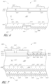
- the heating can be the last heating step in the solar cell fabrication process. In one embodiment, the heating can be the only heating step in the fabrication process. In some embodiments, at least one other heating step can be performed before the heating process of block 106. In one example, the other heating process, aside from the heating process of block 106, can include heating the solar cell to temperature below 900 degrees Celsius. In an example, the heating process below 900 degrees Celsius can be performed before the heating process at 106. In an embodiment, the heating performed at 106 can be performed at the highest temperature among other heating steps performed in the solar cell fabrication process. Figure 3 illustrates the heating process described above.
- the portion 206 of the silicon substrate 202 can be above, as shown, the surface 204 of the silicon substrate 202.
- the heating 230 can getter 232 contaminants 220 from, or nearby, the surface 204 of the silicon substrate 202 and/or from within the silicon substrate 202 to the emitter region 212.
- the heating 230 can getter 232 the containments 220 through the dielectric region 210 to the emitter region 212.
- the solar cell 300 can have a dielectric region 310 formed over the silicon substrate 302.
- the dielectric 310 can be a tunnel oxide.
- the dielectric region 310 can be silicon dioxide.
- the solar cell 300 can have first and second emitter regions 312, 314.
- the first and second emitter regions 312, 314 can be P-type and N-type doped polysilicon regions, respectively.
- impurities and/or contaminants 320 e.g. metal impurities 320 and/or metal contaminants, can be located in the first and second emitter regions 312, 314 as shown.
- the silicon substrate 302 can have some impurities 321 remaining after the gettering process.
- the solar cell 300 can have first and second metal contacts 342, 344 formed on the first and second emitter regions 312, 314, respectively.
- a trench region 305 can be formed, which can separate the first and second emitter regions 312, 314.
- the solar cell 300 can have a textured surface 304 on the front side 301.
- the textured surface 304 can be a surface which can provide additional light absorption.
- the portion 306 of the silicon substrate 302 can be formed above a textured surface 304 as shown.
- the trench region 305 can also be textured, similar to the textured surface 304, for additional light absorption from the back side 303 of the solar cell 300.
- an anti-reflective region (ARC) 318 can be formed over the textured surface 304 of the solar cell 300.
- the anti-reflective region 318 can be silicon nitride.
- impurities and/or contaminants 420 e.g. metal impurities and/or contaminants
- the silicon substrate 402 can have some impurities 421 remaining after the gettering process.
- the dielectric region 510 and second silicon region 514 can be formed over the back side 501 of the solar cell 500.
- the solar cell 500 can have first and second metal contacts 542, 544 formed on the first and second emitter regions 512, 514, respectively.
- the solar cell 500 can have a textured surface 504 on the front side 501 and/or a textured surface 550 on the back side 503 as shown.
- the textured surfaces 504, 550 can be surfaces which can provide additional light absorption.
- the portion 506 of the silicon substrate 502 can be above a textured surface 504 as shown.
- an anti-reflective region 518 can be formed over the textured surface 504 of the solar cell 500.
- Table 1 a table is shown listing Temperature and Surface Dopant Concentration and output results, such as Gettering Location, Surface Passivation, Lifetime and Efficiency, for example processes of fabricating solar cells.
- Example Process C of Table 1 The method of Figures 1-4 is exemplified in Example Process C of Table 1, where a surface, or a portion near the surface, of a silicon substrate was doped at approximately less than or equal to 2 ⁇ 10 18 cm -3 and the solar cell of Example Process C heated to a temperature above 900 degrees Celsius.
- the results from Example Process C are gettering in a polysilicon region of the silicon substrate, improved surface passivation at approximately 5 fA/cm 2 , improved lifetime, e.g. typical of approximately 10 ⁇ sec, and a > 0.5 % efficiency increase as compared to other solar cells, e.g. referenced as the baseline efficiency.
- Figure 8 illustrates a graph of surface passivation measurements from solar cells fabricated using the Example Process A and C from Table 1. As shown, the Example Process C has lower passivation results as compared to Example Process A. Lower surface passivation is preferred for high efficiency solar cells. Thus, the Example Process C has improved surface passivation results as compared to Example Process A.
- Example Process C has higher lifetime, lower 1/lifetime results, as compared to Example Process A. Higher lifetime is preferred for high efficiency solar cells. Thus, the Example Process C has improved lifetime results as compared to Example Process A.
- Figure 10 illustrates a graph of efficiency measurements from solar cells fabricated using the Example Process A and C from Table 1. As shown, the Example Process C has higher efficiency results as compared to Example Process A. Higher solar cell efficiency conversion is preferred to maximize the electricity conversion from collected light. Thus, the Example Process C has improved efficiency results over Example Process A.
Landscapes
- Life Sciences & Earth Sciences (AREA)
- Engineering & Computer Science (AREA)
- Sustainable Energy (AREA)
- Sustainable Development (AREA)
- Photovoltaic Devices (AREA)
- Chemical & Material Sciences (AREA)
- Crystallography & Structural Chemistry (AREA)
- Formation Of Insulating Films (AREA)
Applications Claiming Priority (3)
| Application Number | Priority Date | Filing Date | Title |
|---|---|---|---|
| US14/579,935 US9520507B2 (en) | 2014-12-22 | 2014-12-22 | Solar cells with improved lifetime, passivation and/or efficiency |
| EP15874267.6A EP3238272B1 (de) | 2014-12-22 | 2015-12-21 | Verfahren zur herstellung einer solarzelle mit verbesserter lebensdauer, passivierung und/oder effizienz |
| PCT/US2015/067220 WO2016106252A1 (en) | 2014-12-22 | 2015-12-21 | Solar cells with improved lifetime, passivation and/or efficiency |
Related Parent Applications (2)
| Application Number | Title | Priority Date | Filing Date |
|---|---|---|---|
| EP15874267.6A Division-Into EP3238272B1 (de) | 2014-12-22 | 2015-12-21 | Verfahren zur herstellung einer solarzelle mit verbesserter lebensdauer, passivierung und/oder effizienz |
| EP15874267.6A Division EP3238272B1 (de) | 2014-12-22 | 2015-12-21 | Verfahren zur herstellung einer solarzelle mit verbesserter lebensdauer, passivierung und/oder effizienz |
Publications (2)
| Publication Number | Publication Date |
|---|---|
| EP4398315A2 true EP4398315A2 (de) | 2024-07-10 |
| EP4398315A3 EP4398315A3 (de) | 2024-12-25 |
Family
ID=56130441
Family Applications (3)
| Application Number | Title | Priority Date | Filing Date |
|---|---|---|---|
| EP15874267.6A Active EP3238272B1 (de) | 2014-12-22 | 2015-12-21 | Verfahren zur herstellung einer solarzelle mit verbesserter lebensdauer, passivierung und/oder effizienz |
| EP24176520.5A Pending EP4398315A3 (de) | 2014-12-22 | 2015-12-21 | Solarzellen mit verbesserter lebensdauer, passivierung und/oder effizienz |
| EP24196750.4A Withdrawn EP4447132A3 (de) | 2014-12-22 | 2015-12-21 | Verfahren zur herstellung einer solarzelle mit verbesserter lebensdauer, passivierung und/oder effizienz |
Family Applications Before (1)
| Application Number | Title | Priority Date | Filing Date |
|---|---|---|---|
| EP15874267.6A Active EP3238272B1 (de) | 2014-12-22 | 2015-12-21 | Verfahren zur herstellung einer solarzelle mit verbesserter lebensdauer, passivierung und/oder effizienz |
Family Applications After (1)
| Application Number | Title | Priority Date | Filing Date |
|---|---|---|---|
| EP24196750.4A Withdrawn EP4447132A3 (de) | 2014-12-22 | 2015-12-21 | Verfahren zur herstellung einer solarzelle mit verbesserter lebensdauer, passivierung und/oder effizienz |
Country Status (6)
| Country | Link |
|---|---|
| US (5) | US9520507B2 (de) |
| EP (3) | EP3238272B1 (de) |
| KR (1) | KR102668024B1 (de) |
| CN (2) | CN113224181A (de) |
| ES (1) | ES2991299T3 (de) |
| WO (1) | WO2016106252A1 (de) |
Families Citing this family (3)
| Publication number | Priority date | Publication date | Assignee | Title |
|---|---|---|---|---|
| US11584483B2 (en) | 2010-02-11 | 2023-02-21 | Allen Szydlowski | System for a very large bag (VLB) for transporting liquids powered by solar arrays |
| US9520507B2 (en) | 2014-12-22 | 2016-12-13 | Sunpower Corporation | Solar cells with improved lifetime, passivation and/or efficiency |
| CN110199376A (zh) | 2016-12-06 | 2019-09-03 | 澳大利亚国立大学 | 太阳能电池制造 |
Family Cites Families (49)
| Publication number | Priority date | Publication date | Assignee | Title |
|---|---|---|---|---|
| US7718888B2 (en) | 2005-12-30 | 2010-05-18 | Sunpower Corporation | Solar cell having polymer heterojunction contacts |
| US7425497B2 (en) | 2006-01-20 | 2008-09-16 | International Business Machines Corporation | Introduction of metal impurity to change workfunction of conductive electrodes |
| WO2007112547A1 (en) * | 2006-03-20 | 2007-10-11 | Nortel Networks Limited | Method & system for fractional frequency reuse in a wireless communication network |
| US7737357B2 (en) | 2006-05-04 | 2010-06-15 | Sunpower Corporation | Solar cell having doped semiconductor heterojunction contacts |
| US20080197454A1 (en) | 2007-02-16 | 2008-08-21 | Calisolar, Inc. | Method and system for removing impurities from low-grade crystalline silicon wafers |
| KR20100015622A (ko) * | 2007-03-16 | 2010-02-12 | 비피 코포레이션 노쓰 아메리카 인코포레이티드 | 태양 전지 |
| EP2165371B1 (de) * | 2007-07-18 | 2012-02-29 | Imec | Verfahren zur herstellung einer emitterstruktur und daraus resultierende emitterstrukturen |
| US8207444B2 (en) * | 2008-07-01 | 2012-06-26 | Sunpower Corporation | Front contact solar cell with formed electrically conducting layers on the front side and backside |
| US8124502B2 (en) | 2008-10-23 | 2012-02-28 | Applied Materials, Inc. | Semiconductor device manufacturing method, semiconductor device and semiconductor device manufacturing installation |
| US8242354B2 (en) * | 2008-12-04 | 2012-08-14 | Sunpower Corporation | Backside contact solar cell with formed polysilicon doped regions |
| US20100304527A1 (en) * | 2009-03-03 | 2010-12-02 | Peter Borden | Methods of thermal processing a solar cell |
| MY166305A (en) * | 2009-12-09 | 2018-06-25 | Solexel Inc | High-efficiency photovoltaic back-contact solar cell structures and manufacturing methods using thin planar semiconductor absorbers |
| JP5338702B2 (ja) | 2010-02-12 | 2013-11-13 | 信越化学工業株式会社 | 太陽電池の製造方法 |
| KR101661768B1 (ko) | 2010-09-03 | 2016-09-30 | 엘지전자 주식회사 | 태양전지 및 이의 제조 방법 |
| BR112013006364A2 (pt) * | 2010-09-16 | 2016-06-28 | Specmat Inc | método, processo, e tecnologia de fabricação de células solares de silício cristalino de alta eficiência e baixo custo |
| US20120073650A1 (en) * | 2010-09-24 | 2012-03-29 | David Smith | Method of fabricating an emitter region of a solar cell |
| US8492253B2 (en) * | 2010-12-02 | 2013-07-23 | Sunpower Corporation | Method of forming contacts for a back-contact solar cell |
| CN102157585B (zh) * | 2011-02-28 | 2013-01-23 | 中山大学 | 一种均匀浅发射极太阳电池的制备方法 |
| WO2012132854A1 (ja) | 2011-03-25 | 2012-10-04 | 三洋電機株式会社 | 光電変換装置及びその製造方法 |
| DE102011050214A1 (de) * | 2011-05-09 | 2012-11-15 | Centrotherm Photovoltaics Ag | Verfahren zur Herstellung einer Solarzelle mit einer mehrstufigen Dotierung |
| US9054256B2 (en) | 2011-06-02 | 2015-06-09 | Solarcity Corporation | Tunneling-junction solar cell with copper grid for concentrated photovoltaic application |
| WO2012169319A1 (ja) | 2011-06-06 | 2012-12-13 | 三洋電機株式会社 | 太陽電池の製造方法 |
| TWI559563B (zh) * | 2011-12-21 | 2016-11-21 | 太陽電子公司 | 混合式多晶矽異質接面背接觸電池 |
| US20130247981A1 (en) * | 2012-03-21 | 2013-09-26 | Suniva, Inc. | Solar cell fabrication using a pre-doping dielectric layer |
| US9054255B2 (en) * | 2012-03-23 | 2015-06-09 | Sunpower Corporation | Solar cell having an emitter region with wide bandgap semiconductor material |
| EP2654090B1 (de) * | 2012-04-17 | 2020-07-08 | LG Electronics, Inc. | Solarzelle |
| CN102694077B (zh) * | 2012-06-11 | 2014-08-06 | 林刘毓 | 一种铜铟镓硒薄膜太阳能电池的制备方法 |
| WO2013192559A1 (en) * | 2012-06-22 | 2013-12-27 | Izar Solar Inc | Manufacturing semiconductor-based multi-junction photovoltaic devices |
| US9202959B2 (en) * | 2012-09-25 | 2015-12-01 | International Business Machines Corporation | Embedded junction in hetero-structured back-surface field for photovoltaic devices |
| KR101889775B1 (ko) | 2012-09-27 | 2018-08-20 | 엘지전자 주식회사 | 태양 전지 및 이의 제조 방법 |
| WO2014093816A2 (en) * | 2012-12-13 | 2014-06-19 | Daniel Scott Marshall | Magnetically polarized photonic device |
| US9312406B2 (en) * | 2012-12-19 | 2016-04-12 | Sunpower Corporation | Hybrid emitter all back contact solar cell |
| US8785233B2 (en) * | 2012-12-19 | 2014-07-22 | Sunpower Corporation | Solar cell emitter region fabrication using silicon nano-particles |
| US9018516B2 (en) * | 2012-12-19 | 2015-04-28 | Sunpower Corporation | Solar cell with silicon oxynitride dielectric layer |
| US9812592B2 (en) * | 2012-12-21 | 2017-11-07 | Sunpower Corporation | Metal-foil-assisted fabrication of thin-silicon solar cell |
| US9847438B2 (en) * | 2013-03-15 | 2017-12-19 | Sunpower Corporation | Reduced contact resistance and improved lifetime of solar cells |
| MY175806A (en) * | 2013-03-15 | 2020-07-09 | Sunpower Corp | Conductivity enhancement of solar cells |
| KR102045001B1 (ko) * | 2013-06-05 | 2019-12-02 | 엘지전자 주식회사 | 태양 전지 및 이의 제조 방법 |
| KR102098100B1 (ko) | 2013-09-17 | 2020-04-08 | 엘지이노텍 주식회사 | 태양전지 및 이의 제조 방법 |
| EP3048648B1 (de) | 2013-09-19 | 2019-04-17 | Panasonic Intellectual Property Management Co., Ltd. | Solarzelle und solarzellenmodul |
| DE112014004468B4 (de) | 2013-09-25 | 2022-02-03 | Panasonic Intellectual Property Management Co., Ltd. | Solarzelle, Solarzellenmodul und Solarzellen-Herstellungsverfahren |
| KR20150035295A (ko) | 2013-09-27 | 2015-04-06 | 엘지이노텍 주식회사 | 태양전지 |
| US9401450B2 (en) * | 2013-12-09 | 2016-07-26 | Sunpower Corporation | Solar cell emitter region fabrication using ion implantation |
| CN103904141B (zh) * | 2014-02-20 | 2016-08-24 | 中国科学院电工研究所 | 低表面浓度轻掺杂区选择性发射极结构的制备方法 |
| KR101622091B1 (ko) | 2014-08-20 | 2016-05-18 | 엘지전자 주식회사 | 태양 전지 및 이의 제조 방법 |
| KR20160052270A (ko) | 2014-11-04 | 2016-05-12 | 엘지전자 주식회사 | 태양 전지 |
| US9722104B2 (en) | 2014-11-28 | 2017-08-01 | Lg Electronics Inc. | Solar cell and method for manufacturing the same |
| KR20160064692A (ko) | 2014-11-28 | 2016-06-08 | 엘지전자 주식회사 | 태양 전지 및 그 제조 방법 |
| US9520507B2 (en) * | 2014-12-22 | 2016-12-13 | Sunpower Corporation | Solar cells with improved lifetime, passivation and/or efficiency |
-
2014
- 2014-12-22 US US14/579,935 patent/US9520507B2/en active Active
-
2015
- 2015-12-21 KR KR1020177020250A patent/KR102668024B1/ko active Active
- 2015-12-21 EP EP15874267.6A patent/EP3238272B1/de active Active
- 2015-12-21 WO PCT/US2015/067220 patent/WO2016106252A1/en not_active Ceased
- 2015-12-21 EP EP24176520.5A patent/EP4398315A3/de active Pending
- 2015-12-21 EP EP24196750.4A patent/EP4447132A3/de not_active Withdrawn
- 2015-12-21 ES ES15874267T patent/ES2991299T3/es active Active
- 2015-12-21 CN CN202110491530.0A patent/CN113224181A/zh active Pending
- 2015-12-21 CN CN201580070020.9A patent/CN107112371A/zh active Pending
-
2016
- 2016-07-18 US US15/213,273 patent/US9899542B2/en active Active
-
2018
- 2018-01-22 US US15/876,927 patent/US10170642B2/en active Active
- 2018-12-20 US US16/228,165 patent/US10658525B2/en active Active
-
2020
- 2020-05-18 US US16/877,255 patent/US11251315B2/en active Active
Also Published As
| Publication number | Publication date |
|---|---|
| US9520507B2 (en) | 2016-12-13 |
| US20160329441A1 (en) | 2016-11-10 |
| CN107112371A (zh) | 2017-08-29 |
| US9899542B2 (en) | 2018-02-20 |
| EP3238272C0 (de) | 2024-08-28 |
| US10170642B2 (en) | 2019-01-01 |
| US20180219108A1 (en) | 2018-08-02 |
| EP3238272B1 (de) | 2024-08-28 |
| ES2991299T3 (es) | 2024-12-03 |
| KR102668024B1 (ko) | 2024-05-21 |
| US10658525B2 (en) | 2020-05-19 |
| EP4398315A3 (de) | 2024-12-25 |
| EP3238272A1 (de) | 2017-11-01 |
| EP3238272A4 (de) | 2018-04-11 |
| EP4447132A2 (de) | 2024-10-16 |
| US20160181444A1 (en) | 2016-06-23 |
| US20210043782A1 (en) | 2021-02-11 |
| WO2016106252A1 (en) | 2016-06-30 |
| EP4447132A3 (de) | 2024-12-25 |
| US11251315B2 (en) | 2022-02-15 |
| KR20170100578A (ko) | 2017-09-04 |
| US20190131463A1 (en) | 2019-05-02 |
| CN113224181A (zh) | 2021-08-06 |
Similar Documents
| Publication | Publication Date | Title |
|---|---|---|
| US10840392B2 (en) | Solar cells with tunnel dielectrics | |
| AU2015267299B2 (en) | Relative dopant concentration levels in solar cells | |
| AU2021202377A1 (en) | Improved front contact heterojunction process | |
| KR101886818B1 (ko) | 이종 접합 실리콘 태양 전지의 제조 방법 | |
| US11251315B2 (en) | Solar cells with improved lifetime, passivation and/or efficiency | |
| KR20130082066A (ko) | 광기전력소자 및 제조 방법 | |
| AU2014233535B2 (en) | Reduced contact resistance and improved lifetime of solar cells | |
| KR101159277B1 (ko) | 강유전체를 이용한 태양전지의 제조방법 | |
| US9559236B2 (en) | Solar cell fabricated by simplified deposition process | |
| KR101300803B1 (ko) | 고상성장을 이용한 태양전지 도핑층 형성방법 | |
| JP4185246B2 (ja) | 積層型太陽電池及びその製造方法 | |
| KR20130008913A (ko) | 고상성장을 이용한 태양전지 도핑층 형성방법 |
Legal Events
| Date | Code | Title | Description |
|---|---|---|---|
| PUAI | Public reference made under article 153(3) epc to a published international application that has entered the european phase |
Free format text: ORIGINAL CODE: 0009012 |
|
| STAA | Information on the status of an ep patent application or granted ep patent |
Free format text: STATUS: THE APPLICATION HAS BEEN PUBLISHED |
|
| AC | Divisional application: reference to earlier application |
Ref document number: 3238272 Country of ref document: EP Kind code of ref document: P |
|
| AK | Designated contracting states |
Kind code of ref document: A2 Designated state(s): AL AT BE BG CH CY CZ DE DK EE ES FI FR GB GR HR HU IE IS IT LI LT LU LV MC MK MT NL NO PL PT RO RS SE SI SK SM TR |
|
| PUAL | Search report despatched |
Free format text: ORIGINAL CODE: 0009013 |
|
| AK | Designated contracting states |
Kind code of ref document: A3 Designated state(s): AL AT BE BG CH CY CZ DE DK EE ES FI FR GB GR HR HU IE IS IT LI LT LU LV MC MK MT NL NO PL PT RO RS SE SI SK SM TR |
|
| RIC1 | Information provided on ipc code assigned before grant |
Ipc: H01L 31/0745 20120101ALI20241120BHEP Ipc: H01L 31/068 20120101ALI20241120BHEP Ipc: H01L 31/0224 20060101ALI20241120BHEP Ipc: H01L 31/0216 20140101ALI20241120BHEP Ipc: H01L 31/18 20060101ALI20241120BHEP Ipc: H01L 21/322 20060101ALI20241120BHEP Ipc: H01L 31/0747 20120101AFI20241120BHEP |
|
| STAA | Information on the status of an ep patent application or granted ep patent |
Free format text: STATUS: REQUEST FOR EXAMINATION WAS MADE |
|
| 17P | Request for examination filed |
Effective date: 20250625 |