EP4401005A1 - Support de données portatif - Google Patents
Support de données portatif Download PDFInfo
- Publication number
- EP4401005A1 EP4401005A1 EP23382022.4A EP23382022A EP4401005A1 EP 4401005 A1 EP4401005 A1 EP 4401005A1 EP 23382022 A EP23382022 A EP 23382022A EP 4401005 A1 EP4401005 A1 EP 4401005A1
- Authority
- EP
- European Patent Office
- Prior art keywords
- sealing layer
- data carrier
- lower sealing
- card
- chip module
- Prior art date
- Legal status (The legal status is an assumption and is not a legal conclusion. Google has not performed a legal analysis and makes no representation as to the accuracy of the status listed.)
- Pending
Links
Images
Classifications
-
- G—PHYSICS
- G06—COMPUTING OR CALCULATING; COUNTING
- G06K—GRAPHICAL DATA READING; PRESENTATION OF DATA; RECORD CARRIERS; HANDLING RECORD CARRIERS
- G06K19/00—Record carriers for use with machines and with at least a part designed to carry digital markings
- G06K19/06—Record carriers for use with machines and with at least a part designed to carry digital markings characterised by the kind of the digital marking, e.g. shape, nature, code
- G06K19/067—Record carriers with conductive marks, printed circuits or semiconductor circuit elements, e.g. credit or identity cards also with resonating or responding marks without active components
- G06K19/07—Record carriers with conductive marks, printed circuits or semiconductor circuit elements, e.g. credit or identity cards also with resonating or responding marks without active components with integrated circuit chips
- G06K19/077—Constructional details, e.g. mounting of circuits in the carrier
- G06K19/0772—Physical layout of the record carrier
- G06K19/07726—Physical layout of the record carrier the record comprising means for indicating first use, e.g. a frangible layer
Definitions
- the present invention relates to portable card-shaped data carriers having chip modules with contact surfaces embedded in their card bodies, and to methods for production and use of such data carriers.
- Portable card-shaped data carriers of the above-mentioned type are in circulation by the tens of millions worldwide. They usually have important personal data of legitimate users stored therein, such as names, addresses, account details, access passwords and the like.
- Such card-shaped data carriers are used particularly frequently as bank, debit and credit cards that grant the legitimate user access to his account via a terminal in order to carry out money transfers.
- the terminal reads out personal data via the contact surfaces of the chip module and processes the read-out data, for example by authenticating the user of the data carrier, such as a bank customer, on the basis of the read-out data and giving him access to his account in order to carry out money transfers.
- the aforementioned card-shaped data carriers are sent by regular mail by the card manufacturer or by a card issuer, such as a bank or credit institution, to the legitimate user.
- the user must first subject the data carrier to a validation process, which ensures that the data carrier has reached the legitimate user before the data carrier is allowed for the intended use.
- the user can perform the validation at a suitable terminal or online.
- a fraud scenario that has been known for some years is to intercept the data carrier on its way from the manufacturer or issuer to the legitimate user and to manipulate it before validation by replacing the original chip of the data carrier with a manipulated or an invalid or old chip. After such fraudulent exchange of chips, the manipulated data carrier is then prepared and sent to the user in such a way that the manipulation is only noticed upon validation. Within this time window between manipulation and failed validation, the user's account can be compromised by means of the removed original chip.
- the present invention addresses the improvement of the security of a data carrier of the type mentioned by excluding the fraud scenario described above.
- a card-shaped data carrier is provided with a chip module with contact surfaces embedded in its card body, the chip module of which is covered with a flat seal in such a way that an attacker cannot remove the chip module from the card body and/or exchange it for a manipulated or expired chip module without damaging the seal.
- the inventive seal effectively prevents the attack scenario described above, because manipulation of the chip module or its replacement is no longer possible without the user immediately recognizing this by the damage to the seal.
- the seal is therefore made of a suitable material that prevents the seal from being peeled off the card body without leaving any traces of tampering, such as distortions, tears or other damages, and/or from being applied back onto the card body in the correct position after tampering without leaving any traces of tampering visible to the user.
- the seal is preferably applied to the card body in such a way that it at least partially covers a circumferential edge of the chip module, which delimits the chip module from the card body when viewed from above.
- the seal will be compromised when the chip module is removed from the card body.
- the preferred complete covering of the circumferential edge by the seal even increases this security effect.
- the seal according to the present invention comprises a lower and an upper sealing layer, which are arranged on top of each other on the card body, while each sealing layer causing different security effects that contribute to the overall security gain provided by the present invention.
- the lower sealing layer is applied directly to the card body and/or the chip module, while the upper sealing layer covers the lower sealing layer at least partially, preferably completely.
- the lower sealing layer covers the circumferential edge that delimits the chip module from the card body and leaves the contact surfaces of the chip module uncovered.
- the lower sealing layer ensures two things, namely on the one hand that the chip module cannot be removed without leaving traces of manipulation, and on the other hand that the card-shaped data carrier can be used as intended even though the lower sealing layer is applied to it.
- the upper sealing layer preferably completely covers the chip module and its contact surfaces, so that the user must remove the upper sealing layer before he can use the data carrier as intended.
- the upper sealing layer also completely covers the lower sealing layer so that the latter is not visible as long as the upper sealing layer is not removed.
- the lower sealing layer is preferably made of an anti-peel material that leaves tamper marks as soon as the lower sealing layer is tampered with or attempts are made to remove the lower sealing layer from the data carrier, for example to remove the chip module from the card body.
- the material properties of the anti-peeling material are such that it permanently and irrevocably deforms or distorts the material when attempts are made to remove it from the card body.
- the material of the upper sealing layer is such that it can be removed without damaging the lower sealing layer or the data carrier.
- the upper sealing layer deforms during removal so that it cannot be reapplied to the data carrier unnoticed once it has been removed.
- An attacker according to the above-mentioned scenario can therefore remove neither the upper nor the lower sealing layer without the legitimate user noticing this.
- the user on the other hand, can remove the upper sealing layer for validation and later legitimate use of the data carrier without compromising the protection of the chip module provided by the lower sealing layer.
- the lower sealing layer is preferably transparent or at least designed in such a way that it does not differ or differs as little as possible from the graphic design of the data carrier or the card body. This means that the lower sealing layer is in particular in the same color as the card body.
- the seal or its two sealing layers can be designed in such a way that manipulations not only cause damage or traces to the lower and/or upper sealing layer, but that the chip module and/or the card body also bear traces of manipulation or damage as soon as the lower sealing layer is manipulated or an attempt is made to remove it from the data carrier.
- manipulation marks are, for example, material degeneration or discoloration caused by the lower sealing layer or any adhesive layer.
- the data carrier according to the invention may be a credit or debit card, a payment card, an access card, an identification card or the like, which in particular complies with the relevant standards and norms in connection with chip or payment cards, such as the EMVCo standards.
- a method for manufacturing a card-shaped data carrier according to the first aspect comprises the following two further manufacturing steps, after manufacturing a card-shaped data carrier with chip module:
- the data carrier produced in this way is then delivered to the legitimate user or customer, for example by mail.
- the two aforementioned steps ensure that the above-mentioned fraud scenario is effectively prevented when the data carrier is delivered to the user.
- a card-shaped data carrier according to the invention is finally put into use by the legitimate user by removing the undamaged upper sealing layer, thereby exposing the contact surfaces of the chip module without compromising the protection provided by the lower sealing layer. The user can then validate the data carrier and use it as intended.
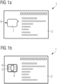
- Fig. 1 shows a card-shaped data carrier 1 in three different configurations.
- Fig. 1c shows a conventional contact-based smart card or chip card 1 as a card-shaped data carrier, in whose plastic card body 2 a chip module 3 is embedded, via whose standardized contact surfaces 4 the chip card 1 can enter into data communication with a suitable terminal, for example with a payment transaction or POS terminal ("point of sale").
- the chip card 1 shown in Fig. 1c is also physically individualized to the legitimate user, which is symbolized by the indicated inscription ("XXX") on the surface of the card body 2, which indicates the name of the user and the card issuer as well as an account number, an expiry date and the like.
- the chip card 1 according to the invention is usually a debit or credit card, a payment card or the like, which generally complies with the relevant norms and standards, such as the EMVCo standard.
- a chip card 1 according to the invention can also provide functions outside financial services, for example in the form of an access or identification card, which is also used by means of contact-based data communication.
- the chip module 3 is inserted into a suitable cavity of the card body 2 and, if necessary, electrically contacted with further structures in the card body 2, for example with an antenna or the like. After the flush insertion of the chip module 3 into the card body 2, a circumferential edge 5 results at the transition between the chip module 3 and the card body 2.
- This circumferential edge 5 demarcates the surface of the chip module 3 from the surface of the card body 2 and forms a point of attack in such fraud or attack scenarios that are based on replacing an original chip module 3, which is usually personalized or electronically individualized to a legitimate user, with a manipulated or expired chip module.
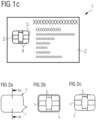
- Fig. 2c shows the chip module 3 with contact surfaces 4 and the circumferential edge 5 in higher resolution.
- the original chip module 3 is replaced by an attacker with another chip module 3 in the associated card body 2, such as a manipulated or expired chip module from another chip card, in such a way that the legitimate user of the chip card 1 does not notice the fraud, or at least not immediately. This then gives the attacker enough time to illegitimately access the user's account using the removed original chip module 3.
- the user notices the fraud, for example when he contacts the card issuer after the failed validation of his chip card 1, the fraud has usually long been completed.
- this attack scenario is prevented by a seal 6, which the attacker must inevitably damage in order to remove the original chip module 3 from the card body 2 and replace it.
- the seal 6 is made of a suitable material that is either damaged during the manipulation or can no longer be applied to the chip card 1 after the manipulation without the user noticing the manipulation immediately.
- Fig. 1a and 1b illustrate the seal 6 according to the invention.
- the seal 6 comprises a lower sealing layer 8 ( Fig. 1b ) and an upper sealing layer 7 ( Fig. 1a ), which completely covers the former and preferably the entire visible chip module 3.
- Fig. 2a and 2b show the respective sealing layers 7, 8 in higher resolution.
- Fig. 1b shows that according to a preferred embodiment, the lower sealing layer 8 is applied to the circumferential edge 5 in such a way that it completely covers the circumferential edge 5 and, along the circumferential edge 5, covers sections of the card body 2 on the one hand and sections of the chip module 3 on the other hand. In this case, however, the contact surfaces 4 of the chip module 3 remain uncovered so that the user can use the chip card 1 in connection with a POS terminal even though the lower sealing layer 8 covers the circumferential edge 5.
- the geometry and two-dimensional design of the lower sealing layer can of course be different from that shown in Fig. 1b , as long as the lower sealing layer 8 fulfils its two functions according to the invention, namely on the one hand the complete or partial covering of the circumferential edge 5 in such a way that the chip module 3 cannot be removed from the card body 2 without permanent damage to the lower sealing layer 8, and on the other hand leaving the contact surfaces 4 free to allow the user to use the chip card 1.
- the lower sealing layer 8 it is possible for the lower sealing layer 8 to cover the circumferential edge 5 only in sections or for the lower sealing layer to cover the card body 2 over a large area or even completely, and then serve as a further protective layer, possibly provided with additional security features, while the contact surfaces 4 remain accessible.
- the lower sealing layer 8 is therefore preferably transparent or at least reproduces the color scheme and design of the card body 2 in such a way that the lower sealing layer 8 is not, or at least not immediately, noticeable to the untrained observer.
- Fig. 1a shows that according to a preferred embodiment, the upper sealing layer 7 completely covers the lower sealing layer 8 and the chip module 4.
- the function of the upper sealing layer 7 is that it covers at least the contact surfaces 4 in such a way that the chip card 1 cannot be used without first peeling off the upper sealing layer 7.
- the geometry and two-dimensional design of the upper sealing layer 7 can of course be different from that shown in Fig. 1a , as long as the upper sealing layer 7 fulfils its two functions according to the invention, namely to prevent immediate use of the chip card 1 on the one hand and to protect the contact surfaces 4 during postal dispatch on the other.
- the upper sealing layer 7 does not completely cover the lower sealing layer 8 and/or that the contact surfaces 4 are only covered in such a way that immediate use of the chip card 1 is precluded.
- the upper sealing layer 7 can be designed as a grid or mesh pattern or the like.
- the materials and the geometries of the upper and lower sealing layers 7, 8 are selected according to the invention in such a way that the chip module 3 cannot be removed from the card body 2 without damaging the seal 6.
- the upper sealing layer 7 and the lower sealing layer 8 are designed in such a way that the upper sealing layer 7 can be removed without damaging the lower sealing layer 8 or the data carrier 1 or its card body 2, but it can then no longer be applied to the card body 2 without it being obvious that it has already been removed.
- the material of the upper sealing layer 7 and/or the adhesion or an adhesive layer between the upper and lower sealing layers 7, 8 is thus selected in such a way that the upper sealing layer 7 deforms, tears or is otherwise irreversibly deformed when it is removed from the card body 2, but that on the other hand it does not impair the lower sealing layer 8 and the card body 2 or the chip module 3 in any way.
- the material of the lower sealing layer 8 in turn is preferably an anti-peel material that cannot be removed from the card body 2 for the purpose of exposing the circumferential edge 6 without leaving manipulation marks or damage. These manipulation marks or damages preferably occur at the lower sealing layer 8, but can also become additionally visible at the card body 2 and/or at the chip module 3.
- the material of the lower sealing layer 8 and/or the adhesion or an adhesive layer between the lower sealing layer 8 and the card body 2/chip module 3 is thus selected in such a way that the lower sealing layer 8 deforms, tears or is otherwise irreversibly deformed when it is peeled off from the circumferential edge 5, but that on the other hand it remains unaffected by the peeling off of the upper sealing layer 7.
- the lower sealing layer 8 also leaves traces, such as adhesions, material degenerations or discolorations in the card body 2 and/or the chip module 3, so that a completely missing lower sealing layer 8 is nevertheless recognized by the legitimate user on the basis of these manipulation traces in the card body 2 and/or on the chip module 3.
- traces such as adhesions, material degenerations or discolorations in the card body 2 and/or the chip module 3.
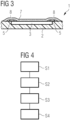
- Fig. 3 shows a cross-sectional view through the chip module according to Fig. 2a along line III-III.
- the dimensions of the illustrated sections of the lower and upper sealing layers 7, 8 do not correspond to reality, but are designed in such a way that the invention can be clearly seen from Fig. 3 .
- Fig. 3 also shows that the lower sealing layer 8 covers the circumferential edge 5, but leaves the contact surfaces of the chip module 3 free.
- the upper sealing layer 7 covers the chip module 3 as well as the shown sections of the lower sealing layer 8. The curvature of the upper sealing layer 7 when passing over the lower sealing layer 8 will hardly or not at all be visible in reality, depending on the material of the upper sealing layer 8.
- Fig. 4 illustrates a manufacturing and use method concerning the chip card 1 according to the invention as shown in Figs. 1 to 3 .
- the lower sealing layer 8 is applied to the card body 2 of a chip card 1 according to Fig. 1c in such a way that it at least partially covers the circumferential edge 5 of the chip module 3.
- a chip card according to Fig. 1b is present.
- step S2 the upper sealing layer 7 is applied to the card body 2 in such a way that it completely covers the lower sealing layer 8.
- a chip card 1 according to Fig. 1a is present.
- step S3 the chip card 1 as shown in Fig. 1a is sent by post from the card manufacturer to the legitimate user.
- the invention has an effect on the fraud and forgery protection of the chip card 1, because an attack based on the replacement of the chip module 3 is not possible without being immediately detected by the user.
- any attempt to remove the chip module 3 without authorization will result in damage to the seal 6.
- both the upper sealing layer 7 and the lower sealing layer 8 and/or the card body 2 and/or the chip module 3 will be impaired or even damaged, because an attacker can only expose the circumferential edge 5 if he removes both sealing layers 7, 8.
- the materials of the sealing layers 7, 8 and/or any adhesive layers are chosen in such a way that the sealing layers 7, 8 are damaged or deformed and can no longer be applied to the card body 2 in the original way.
- step S4 the user removes the upper sealing layer 7, leaving the lower sealing layer 8 unaffected on the card body 2.
- the user can now validate the chip card 1 and then use them as intended for payment transfers or the like.
Landscapes
- Engineering & Computer Science (AREA)
- Computer Hardware Design (AREA)
- Microelectronics & Electronic Packaging (AREA)
- Physics & Mathematics (AREA)
- General Physics & Mathematics (AREA)
- Theoretical Computer Science (AREA)
- Credit Cards Or The Like (AREA)
Priority Applications (1)
| Application Number | Priority Date | Filing Date | Title |
|---|---|---|---|
| EP23382022.4A EP4401005A1 (fr) | 2023-01-12 | 2023-01-12 | Support de données portatif |
Applications Claiming Priority (1)
| Application Number | Priority Date | Filing Date | Title |
|---|---|---|---|
| EP23382022.4A EP4401005A1 (fr) | 2023-01-12 | 2023-01-12 | Support de données portatif |
Publications (1)
| Publication Number | Publication Date |
|---|---|
| EP4401005A1 true EP4401005A1 (fr) | 2024-07-17 |
Family
ID=84981332
Family Applications (1)
| Application Number | Title | Priority Date | Filing Date |
|---|---|---|---|
| EP23382022.4A Pending EP4401005A1 (fr) | 2023-01-12 | 2023-01-12 | Support de données portatif |
Country Status (1)
| Country | Link |
|---|---|
| EP (1) | EP4401005A1 (fr) |
Citations (9)
| Publication number | Priority date | Publication date | Assignee | Title |
|---|---|---|---|---|
| DE19530608A1 (de) * | 1995-08-21 | 1997-02-27 | Orga Kartensysteme Gmbh | Sicherheitschipkarte |
| US5635702A (en) * | 1994-06-24 | 1997-06-03 | Schlumberger Industries | Memory card with a protective layer on the metal electrical contact zone |
| DE19733876A1 (de) * | 1997-08-05 | 1999-02-18 | Winter Wertdruck Gmbh | Datenträger sowie Verwendung desselben und Verfahren zu dessen Herstellung |
| US6371378B1 (en) * | 1997-12-15 | 2002-04-16 | Gemplus | Smart card provided with guarantee label |
| DE10328133A1 (de) * | 2003-06-23 | 2005-01-13 | Giesecke & Devrient Gmbh | Datenträger |
| EP2339511A1 (fr) * | 2009-12-17 | 2011-06-29 | Gemalto SA | Objet communicant avec sécurisation d'une interface de communication par contact |
| DE102011011910A1 (de) * | 2011-02-21 | 2012-08-23 | Giesecke & Devrient Gmbh | Inbetriebnahme eines portablen Datenträgers |
| US20150129662A1 (en) * | 2012-05-18 | 2015-05-14 | Louis Rinze Henricus Adrianus Willemsen | Chip card device and method for manufacture thereof |
| US20190073577A1 (en) * | 2017-07-05 | 2019-03-07 | Travel Tags, Inc. | Stored value card systems with tamper evident activation indicia |
-
2023
- 2023-01-12 EP EP23382022.4A patent/EP4401005A1/fr active Pending
Patent Citations (9)
| Publication number | Priority date | Publication date | Assignee | Title |
|---|---|---|---|---|
| US5635702A (en) * | 1994-06-24 | 1997-06-03 | Schlumberger Industries | Memory card with a protective layer on the metal electrical contact zone |
| DE19530608A1 (de) * | 1995-08-21 | 1997-02-27 | Orga Kartensysteme Gmbh | Sicherheitschipkarte |
| DE19733876A1 (de) * | 1997-08-05 | 1999-02-18 | Winter Wertdruck Gmbh | Datenträger sowie Verwendung desselben und Verfahren zu dessen Herstellung |
| US6371378B1 (en) * | 1997-12-15 | 2002-04-16 | Gemplus | Smart card provided with guarantee label |
| DE10328133A1 (de) * | 2003-06-23 | 2005-01-13 | Giesecke & Devrient Gmbh | Datenträger |
| EP2339511A1 (fr) * | 2009-12-17 | 2011-06-29 | Gemalto SA | Objet communicant avec sécurisation d'une interface de communication par contact |
| DE102011011910A1 (de) * | 2011-02-21 | 2012-08-23 | Giesecke & Devrient Gmbh | Inbetriebnahme eines portablen Datenträgers |
| US20150129662A1 (en) * | 2012-05-18 | 2015-05-14 | Louis Rinze Henricus Adrianus Willemsen | Chip card device and method for manufacture thereof |
| US20190073577A1 (en) * | 2017-07-05 | 2019-03-07 | Travel Tags, Inc. | Stored value card systems with tamper evident activation indicia |
Similar Documents
| Publication | Publication Date | Title |
|---|---|---|
| US8461961B2 (en) | Tamper-proof secure card with stored biometric data and method for using the secure card | |
| EP2497093B1 (fr) | Carte a codes eclaires a utiliser dans des transactions securisees | |
| US5365046A (en) | Preventing unauthorized use of a credit card | |
| US5648647A (en) | Anti-fraud credit card dispatch system | |
| US6068192A (en) | Tamper resistant smart card and method of protecting data in a smart card | |
| US20090199004A1 (en) | System and method for self-authenticating token | |
| US7374098B2 (en) | Chip card including tamper-proof security features | |
| US8690067B2 (en) | Smart card comprising an electronic module supported on a card body provided with a means for authenticating the peering of the module with the body | |
| CN101322143A (zh) | 具有密码输入键的卡 | |
| US10373040B2 (en) | Stored value card systems with tamper evident activation indicia | |
| US10915806B2 (en) | Payment card and method of manufacturing the same | |
| CN1037877C (zh) | 磁卡 | |
| EP4401005A1 (fr) | Support de données portatif | |
| EP1603075A1 (fr) | Procede de stockage de donnees de capacite, differents systemes mettant ce procede en oeuvre, et differents articles | |
| ES2992093T3 (es) | Dispositivo y procedimiento para asegurar los datos de seguridad de una tarjeta de pago bancario | |
| JP2001052143A (ja) | 認証用記録媒体および認証システム | |
| US20060092476A1 (en) | Document with user authentication | |
| US20030018894A1 (en) | System for memorabilia encapsulation and authentication | |
| GB2345175A (en) | Payment card authentication | |
| EP0642098A2 (fr) | Carte de services financiers à l'épreuve de fraudes et de contrefaçon | |
| EP1162581A1 (fr) | Carte de paiement securisé et système avec appareil d'authentification à distance | |
| JPH05159118A (ja) | 可搬型記憶装置、可搬型記憶装置の認証装置及び認証方法 | |
| OA20199A (en) | Device and method for securing secure data for a bank payment card. | |
| WO2019206549A1 (fr) | Étiquette de sécurité pour protéger des codes | |
| JPH08249433A (ja) | プリペイドカードの不正防止方法 |
Legal Events
| Date | Code | Title | Description |
|---|---|---|---|
| PUAI | Public reference made under article 153(3) epc to a published international application that has entered the european phase |
Free format text: ORIGINAL CODE: 0009012 |
|
| STAA | Information on the status of an ep patent application or granted ep patent |
Free format text: STATUS: THE APPLICATION HAS BEEN PUBLISHED |
|
| AK | Designated contracting states |
Kind code of ref document: A1 Designated state(s): AL AT BE BG CH CY CZ DE DK EE ES FI FR GB GR HR HU IE IS IT LI LT LU LV MC ME MK MT NL NO PL PT RO RS SE SI SK SM TR |
|
| STAA | Information on the status of an ep patent application or granted ep patent |
Free format text: STATUS: REQUEST FOR EXAMINATION WAS MADE |
|
| 17P | Request for examination filed |
Effective date: 20250117 |
|
| STAA | Information on the status of an ep patent application or granted ep patent |
Free format text: STATUS: EXAMINATION IS IN PROGRESS |
|
| 17Q | First examination report despatched |
Effective date: 20251105 |