EP4410911A1 - Compositions d'encre et films renfermant des matériaux luminophores à émission à bande étroite - Google Patents
Compositions d'encre et films renfermant des matériaux luminophores à émission à bande étroite Download PDFInfo
- Publication number
- EP4410911A1 EP4410911A1 EP24160690.4A EP24160690A EP4410911A1 EP 4410911 A1 EP4410911 A1 EP 4410911A1 EP 24160690 A EP24160690 A EP 24160690A EP 4410911 A1 EP4410911 A1 EP 4410911A1
- Authority
- EP
- European Patent Office
- Prior art keywords
- pfs
- phosphor
- sample
- film
- narrow band
- Prior art date
- Legal status (The legal status is an assumption and is not a legal conclusion. Google has not performed a legal analysis and makes no representation as to the accuracy of the status listed.)
- Pending
Links
Images


Classifications
-
- C—CHEMISTRY; METALLURGY
- C09—DYES; PAINTS; POLISHES; NATURAL RESINS; ADHESIVES; COMPOSITIONS NOT OTHERWISE PROVIDED FOR; APPLICATIONS OF MATERIALS NOT OTHERWISE PROVIDED FOR
- C09D—COATING COMPOSITIONS, e.g. PAINTS, VARNISHES OR LACQUERS; FILLING PASTES; CHEMICAL PAINT OR INK REMOVERS; INKS; CORRECTING FLUIDS; WOODSTAINS; PASTES OR SOLIDS FOR COLOURING OR PRINTING; USE OF MATERIALS THEREFOR
- C09D11/00—Inks
- C09D11/30—Inkjet printing inks
- C09D11/38—Inkjet printing inks characterised by non-macromolecular additives other than solvents, pigments or dyes
-
- C—CHEMISTRY; METALLURGY
- C09—DYES; PAINTS; POLISHES; NATURAL RESINS; ADHESIVES; COMPOSITIONS NOT OTHERWISE PROVIDED FOR; APPLICATIONS OF MATERIALS NOT OTHERWISE PROVIDED FOR
- C09D—COATING COMPOSITIONS, e.g. PAINTS, VARNISHES OR LACQUERS; FILLING PASTES; CHEMICAL PAINT OR INK REMOVERS; INKS; CORRECTING FLUIDS; WOODSTAINS; PASTES OR SOLIDS FOR COLOURING OR PRINTING; USE OF MATERIALS THEREFOR
- C09D11/00—Inks
- C09D11/02—Printing inks
- C09D11/03—Printing inks characterised by features other than the chemical nature of the binder
- C09D11/037—Printing inks characterised by features other than the chemical nature of the binder characterised by the pigment
-
- C—CHEMISTRY; METALLURGY
- C09—DYES; PAINTS; POLISHES; NATURAL RESINS; ADHESIVES; COMPOSITIONS NOT OTHERWISE PROVIDED FOR; APPLICATIONS OF MATERIALS NOT OTHERWISE PROVIDED FOR
- C09D—COATING COMPOSITIONS, e.g. PAINTS, VARNISHES OR LACQUERS; FILLING PASTES; CHEMICAL PAINT OR INK REMOVERS; INKS; CORRECTING FLUIDS; WOODSTAINS; PASTES OR SOLIDS FOR COLOURING OR PRINTING; USE OF MATERIALS THEREFOR
- C09D11/00—Inks
- C09D11/30—Inkjet printing inks
- C09D11/32—Inkjet printing inks characterised by colouring agents
- C09D11/322—Pigment inks
-
- C—CHEMISTRY; METALLURGY
- C09—DYES; PAINTS; POLISHES; NATURAL RESINS; ADHESIVES; COMPOSITIONS NOT OTHERWISE PROVIDED FOR; APPLICATIONS OF MATERIALS NOT OTHERWISE PROVIDED FOR
- C09D—COATING COMPOSITIONS, e.g. PAINTS, VARNISHES OR LACQUERS; FILLING PASTES; CHEMICAL PAINT OR INK REMOVERS; INKS; CORRECTING FLUIDS; WOODSTAINS; PASTES OR SOLIDS FOR COLOURING OR PRINTING; USE OF MATERIALS THEREFOR
- C09D11/00—Inks
- C09D11/50—Sympathetic, colour changing or similar inks
-
- C—CHEMISTRY; METALLURGY
- C09—DYES; PAINTS; POLISHES; NATURAL RESINS; ADHESIVES; COMPOSITIONS NOT OTHERWISE PROVIDED FOR; APPLICATIONS OF MATERIALS NOT OTHERWISE PROVIDED FOR
- C09D—COATING COMPOSITIONS, e.g. PAINTS, VARNISHES OR LACQUERS; FILLING PASTES; CHEMICAL PAINT OR INK REMOVERS; INKS; CORRECTING FLUIDS; WOODSTAINS; PASTES OR SOLIDS FOR COLOURING OR PRINTING; USE OF MATERIALS THEREFOR
- C09D11/00—Inks
- C09D11/52—Electrically conductive inks
-
- C—CHEMISTRY; METALLURGY
- C09—DYES; PAINTS; POLISHES; NATURAL RESINS; ADHESIVES; COMPOSITIONS NOT OTHERWISE PROVIDED FOR; APPLICATIONS OF MATERIALS NOT OTHERWISE PROVIDED FOR
- C09K—MATERIALS FOR MISCELLANEOUS APPLICATIONS, NOT PROVIDED FOR ELSEWHERE
- C09K11/00—Luminescent materials, e.g. electroluminescent or chemiluminescent
- C09K11/02—Use of particular materials as binders, particle coatings or suspension media therefor
- C09K11/025—Use of particular materials as binders, particle coatings or suspension media therefor non-luminescent particle coatings or suspension media
-
- C—CHEMISTRY; METALLURGY
- C09—DYES; PAINTS; POLISHES; NATURAL RESINS; ADHESIVES; COMPOSITIONS NOT OTHERWISE PROVIDED FOR; APPLICATIONS OF MATERIALS NOT OTHERWISE PROVIDED FOR
- C09K—MATERIALS FOR MISCELLANEOUS APPLICATIONS, NOT PROVIDED FOR ELSEWHERE
- C09K11/00—Luminescent materials, e.g. electroluminescent or chemiluminescent
- C09K11/08—Luminescent materials, e.g. electroluminescent or chemiluminescent containing inorganic luminescent materials
- C09K11/61—Luminescent materials, e.g. electroluminescent or chemiluminescent containing inorganic luminescent materials containing fluorine, chlorine, bromine, iodine or unspecified halogen elements
- C09K11/617—Silicates
-
- C—CHEMISTRY; METALLURGY
- C09—DYES; PAINTS; POLISHES; NATURAL RESINS; ADHESIVES; COMPOSITIONS NOT OTHERWISE PROVIDED FOR; APPLICATIONS OF MATERIALS NOT OTHERWISE PROVIDED FOR
- C09K—MATERIALS FOR MISCELLANEOUS APPLICATIONS, NOT PROVIDED FOR ELSEWHERE
- C09K11/00—Luminescent materials, e.g. electroluminescent or chemiluminescent
- C09K11/08—Luminescent materials, e.g. electroluminescent or chemiluminescent containing inorganic luminescent materials
- C09K11/70—Luminescent materials, e.g. electroluminescent or chemiluminescent containing inorganic luminescent materials containing phosphorus
- C09K11/71—Luminescent materials, e.g. electroluminescent or chemiluminescent containing inorganic luminescent materials containing phosphorus also containing alkaline earth metals
-
- C—CHEMISTRY; METALLURGY
- C09—DYES; PAINTS; POLISHES; NATURAL RESINS; ADHESIVES; COMPOSITIONS NOT OTHERWISE PROVIDED FOR; APPLICATIONS OF MATERIALS NOT OTHERWISE PROVIDED FOR
- C09K—MATERIALS FOR MISCELLANEOUS APPLICATIONS, NOT PROVIDED FOR ELSEWHERE
- C09K11/00—Luminescent materials, e.g. electroluminescent or chemiluminescent
- C09K11/08—Luminescent materials, e.g. electroluminescent or chemiluminescent containing inorganic luminescent materials
- C09K11/70—Luminescent materials, e.g. electroluminescent or chemiluminescent containing inorganic luminescent materials containing phosphorus
- C09K11/71—Luminescent materials, e.g. electroluminescent or chemiluminescent containing inorganic luminescent materials containing phosphorus also containing alkaline earth metals
- C09K11/717—Aluminates; Silicates
-
- F—MECHANICAL ENGINEERING; LIGHTING; HEATING; WEAPONS; BLASTING
- F21—LIGHTING
- F21V—FUNCTIONAL FEATURES OR DETAILS OF LIGHTING DEVICES OR SYSTEMS THEREOF; STRUCTURAL COMBINATIONS OF LIGHTING DEVICES WITH OTHER ARTICLES, NOT OTHERWISE PROVIDED FOR
- F21V9/00—Elements for modifying spectral properties, polarisation or intensity of the light emitted, e.g. filters
- F21V9/30—Elements containing photoluminescent material distinct from or spaced from the light source
-
- G—PHYSICS
- G02—OPTICS
- G02B—OPTICAL ELEMENTS, SYSTEMS OR APPARATUS
- G02B6/00—Light guides; Structural details of arrangements comprising light guides and other optical elements, e.g. couplings
- G02B6/0001—Light guides; Structural details of arrangements comprising light guides and other optical elements, e.g. couplings specially adapted for lighting devices or systems
- G02B6/0011—Light guides; Structural details of arrangements comprising light guides and other optical elements, e.g. couplings specially adapted for lighting devices or systems the light guides being planar or of plate-like form
- G02B6/0033—Means for improving the coupling-out of light from the light guide
- G02B6/005—Means for improving the coupling-out of light from the light guide provided by one optical element, or plurality thereof, placed on the light output side of the light guide
- G02B6/0053—Prismatic sheet or layer; Brightness enhancement element, sheet or layer
-
- G—PHYSICS
- G02—OPTICS
- G02B—OPTICAL ELEMENTS, SYSTEMS OR APPARATUS
- G02B6/00—Light guides; Structural details of arrangements comprising light guides and other optical elements, e.g. couplings
- G02B6/0001—Light guides; Structural details of arrangements comprising light guides and other optical elements, e.g. couplings specially adapted for lighting devices or systems
- G02B6/0011—Light guides; Structural details of arrangements comprising light guides and other optical elements, e.g. couplings specially adapted for lighting devices or systems the light guides being planar or of plate-like form
- G02B6/0066—Light guides; Structural details of arrangements comprising light guides and other optical elements, e.g. couplings specially adapted for lighting devices or systems the light guides being planar or of plate-like form characterised by the light source being coupled to the light guide
- G02B6/0073—Light emitting diode [LED]
-
- G—PHYSICS
- G02—OPTICS
- G02F—OPTICAL DEVICES OR ARRANGEMENTS FOR THE CONTROL OF LIGHT BY MODIFICATION OF THE OPTICAL PROPERTIES OF THE MEDIA OF THE ELEMENTS INVOLVED THEREIN; NON-LINEAR OPTICS; FREQUENCY-CHANGING OF LIGHT; OPTICAL LOGIC ELEMENTS; OPTICAL ANALOGUE/DIGITAL CONVERTERS
- G02F1/00—Devices or arrangements for the control of the intensity, colour, phase, polarisation or direction of light arriving from an independent light source, e.g. switching, gating or modulating; Non-linear optics
- G02F1/01—Devices or arrangements for the control of the intensity, colour, phase, polarisation or direction of light arriving from an independent light source, e.g. switching, gating or modulating; Non-linear optics for the control of the intensity, phase, polarisation or colour
- G02F1/13—Devices or arrangements for the control of the intensity, colour, phase, polarisation or direction of light arriving from an independent light source, e.g. switching, gating or modulating; Non-linear optics for the control of the intensity, phase, polarisation or colour based on liquid crystals, e.g. single liquid crystal display cells
- G02F1/133—Constructional arrangements; Operation of liquid crystal cells; Circuit arrangements
- G02F1/1333—Constructional arrangements; Manufacturing methods
- G02F1/1335—Structural association of cells with optical devices, e.g. polarisers or reflectors
- G02F1/1336—Illuminating devices
- G02F1/133602—Direct backlight
- G02F1/133603—Direct backlight with LEDs
-
- G—PHYSICS
- G02—OPTICS
- G02F—OPTICAL DEVICES OR ARRANGEMENTS FOR THE CONTROL OF LIGHT BY MODIFICATION OF THE OPTICAL PROPERTIES OF THE MEDIA OF THE ELEMENTS INVOLVED THEREIN; NON-LINEAR OPTICS; FREQUENCY-CHANGING OF LIGHT; OPTICAL LOGIC ELEMENTS; OPTICAL ANALOGUE/DIGITAL CONVERTERS
- G02F1/00—Devices or arrangements for the control of the intensity, colour, phase, polarisation or direction of light arriving from an independent light source, e.g. switching, gating or modulating; Non-linear optics
- G02F1/01—Devices or arrangements for the control of the intensity, colour, phase, polarisation or direction of light arriving from an independent light source, e.g. switching, gating or modulating; Non-linear optics for the control of the intensity, phase, polarisation or colour
- G02F1/13—Devices or arrangements for the control of the intensity, colour, phase, polarisation or direction of light arriving from an independent light source, e.g. switching, gating or modulating; Non-linear optics for the control of the intensity, phase, polarisation or colour based on liquid crystals, e.g. single liquid crystal display cells
- G02F1/133—Constructional arrangements; Operation of liquid crystal cells; Circuit arrangements
- G02F1/1333—Constructional arrangements; Manufacturing methods
- G02F1/1335—Structural association of cells with optical devices, e.g. polarisers or reflectors
- G02F1/1336—Illuminating devices
- G02F1/133617—Illumination with ultraviolet light; Luminescent elements or materials associated to the cell
-
- G—PHYSICS
- G03—PHOTOGRAPHY; CINEMATOGRAPHY; ANALOGOUS TECHNIQUES USING WAVES OTHER THAN OPTICAL WAVES; ELECTROGRAPHY; HOLOGRAPHY
- G03F—PHOTOMECHANICAL PRODUCTION OF TEXTURED OR PATTERNED SURFACES, e.g. FOR PRINTING, FOR PROCESSING OF SEMICONDUCTOR DEVICES; MATERIALS THEREFOR; ORIGINALS THEREFOR; APPARATUS SPECIALLY ADAPTED THEREFOR
- G03F7/00—Photomechanical, e.g. photolithographic, production of textured or patterned surfaces, e.g. printing surfaces; Materials therefor, e.g. comprising photoresists; Apparatus specially adapted therefor
- G03F7/004—Photosensitive materials
- G03F7/0042—Photosensitive materials with inorganic or organometallic light-sensitive compounds not otherwise provided for, e.g. inorganic resists
-
- H—ELECTRICITY
- H10—SEMICONDUCTOR DEVICES; ELECTRIC SOLID-STATE DEVICES NOT OTHERWISE PROVIDED FOR
- H10H—INORGANIC LIGHT-EMITTING SEMICONDUCTOR DEVICES HAVING POTENTIAL BARRIERS
- H10H20/00—Individual inorganic light-emitting semiconductor devices having potential barriers, e.g. light-emitting diodes [LED]
- H10H20/80—Constructional details
- H10H20/85—Packages
- H10H20/851—Wavelength conversion means
- H10H20/8511—Wavelength conversion means characterised by their material, e.g. binder
- H10H20/8512—Wavelength conversion materials
-
- H—ELECTRICITY
- H10—SEMICONDUCTOR DEVICES; ELECTRIC SOLID-STATE DEVICES NOT OTHERWISE PROVIDED FOR
- H10H—INORGANIC LIGHT-EMITTING SEMICONDUCTOR DEVICES HAVING POTENTIAL BARRIERS
- H10H20/00—Individual inorganic light-emitting semiconductor devices having potential barriers, e.g. light-emitting diodes [LED]
- H10H20/80—Constructional details
- H10H20/85—Packages
- H10H20/851—Wavelength conversion means
- H10H20/8511—Wavelength conversion means characterised by their material, e.g. binder
- H10H20/8512—Wavelength conversion materials
- H10H20/8513—Wavelength conversion materials having two or more wavelength conversion materials
-
- C—CHEMISTRY; METALLURGY
- C08—ORGANIC MACROMOLECULAR COMPOUNDS; THEIR PREPARATION OR CHEMICAL WORKING-UP; COMPOSITIONS BASED THEREON
- C08K—Use of inorganic or non-macromolecular organic substances as compounding ingredients
- C08K3/00—Use of inorganic substances as compounding ingredients
- C08K3/32—Phosphorus-containing compounds
- C08K2003/321—Phosphates
- C08K2003/328—Phosphates of heavy metals
-
- C—CHEMISTRY; METALLURGY
- C08—ORGANIC MACROMOLECULAR COMPOUNDS; THEIR PREPARATION OR CHEMICAL WORKING-UP; COMPOSITIONS BASED THEREON
- C08K—Use of inorganic or non-macromolecular organic substances as compounding ingredients
- C08K2201/00—Specific properties of additives
- C08K2201/001—Conductive additives
-
- C—CHEMISTRY; METALLURGY
- C08—ORGANIC MACROMOLECULAR COMPOUNDS; THEIR PREPARATION OR CHEMICAL WORKING-UP; COMPOSITIONS BASED THEREON
- C08K—Use of inorganic or non-macromolecular organic substances as compounding ingredients
- C08K2201/00—Specific properties of additives
- C08K2201/002—Physical properties
- C08K2201/005—Additives being defined by their particle size in general
-
- C—CHEMISTRY; METALLURGY
- C08—ORGANIC MACROMOLECULAR COMPOUNDS; THEIR PREPARATION OR CHEMICAL WORKING-UP; COMPOSITIONS BASED THEREON
- C08K—Use of inorganic or non-macromolecular organic substances as compounding ingredients
- C08K3/00—Use of inorganic substances as compounding ingredients
- C08K3/34—Silicon-containing compounds
-
- F—MECHANICAL ENGINEERING; LIGHTING; HEATING; WEAPONS; BLASTING
- F21—LIGHTING
- F21Y—INDEXING SCHEME ASSOCIATED WITH SUBCLASSES F21K, F21L, F21S and F21V, RELATING TO THE FORM OR THE KIND OF THE LIGHT SOURCES OR OF THE COLOUR OF THE LIGHT EMITTED
- F21Y2115/00—Light-generating elements of semiconductor light sources
- F21Y2115/10—Light-emitting diodes [LED]
-
- G—PHYSICS
- G02—OPTICS
- G02B—OPTICAL ELEMENTS, SYSTEMS OR APPARATUS
- G02B3/00—Simple or compound lenses
- G02B3/0006—Arrays
- G02B3/0037—Arrays characterized by the distribution or form of lenses
- G02B3/005—Arrays characterized by the distribution or form of lenses arranged along a single direction only, e.g. lenticular sheets
-
- G—PHYSICS
- G02—OPTICS
- G02B—OPTICAL ELEMENTS, SYSTEMS OR APPARATUS
- G02B6/00—Light guides; Structural details of arrangements comprising light guides and other optical elements, e.g. couplings
- G02B6/0001—Light guides; Structural details of arrangements comprising light guides and other optical elements, e.g. couplings specially adapted for lighting devices or systems
- G02B6/0011—Light guides; Structural details of arrangements comprising light guides and other optical elements, e.g. couplings specially adapted for lighting devices or systems the light guides being planar or of plate-like form
- G02B6/0033—Means for improving the coupling-out of light from the light guide
- G02B6/005—Means for improving the coupling-out of light from the light guide provided by one optical element, or plurality thereof, placed on the light output side of the light guide
-
- G—PHYSICS
- G02—OPTICS
- G02B—OPTICAL ELEMENTS, SYSTEMS OR APPARATUS
- G02B6/00—Light guides; Structural details of arrangements comprising light guides and other optical elements, e.g. couplings
- G02B6/0001—Light guides; Structural details of arrangements comprising light guides and other optical elements, e.g. couplings specially adapted for lighting devices or systems
- G02B6/0011—Light guides; Structural details of arrangements comprising light guides and other optical elements, e.g. couplings specially adapted for lighting devices or systems the light guides being planar or of plate-like form
- G02B6/0065—Manufacturing aspects; Material aspects
-
- G—PHYSICS
- G02—OPTICS
- G02F—OPTICAL DEVICES OR ARRANGEMENTS FOR THE CONTROL OF LIGHT BY MODIFICATION OF THE OPTICAL PROPERTIES OF THE MEDIA OF THE ELEMENTS INVOLVED THEREIN; NON-LINEAR OPTICS; FREQUENCY-CHANGING OF LIGHT; OPTICAL LOGIC ELEMENTS; OPTICAL ANALOGUE/DIGITAL CONVERTERS
- G02F1/00—Devices or arrangements for the control of the intensity, colour, phase, polarisation or direction of light arriving from an independent light source, e.g. switching, gating or modulating; Non-linear optics
- G02F1/01—Devices or arrangements for the control of the intensity, colour, phase, polarisation or direction of light arriving from an independent light source, e.g. switching, gating or modulating; Non-linear optics for the control of the intensity, phase, polarisation or colour
- G02F1/13—Devices or arrangements for the control of the intensity, colour, phase, polarisation or direction of light arriving from an independent light source, e.g. switching, gating or modulating; Non-linear optics for the control of the intensity, phase, polarisation or colour based on liquid crystals, e.g. single liquid crystal display cells
- G02F1/133—Constructional arrangements; Operation of liquid crystal cells; Circuit arrangements
- G02F1/1333—Constructional arrangements; Manufacturing methods
- G02F1/1335—Structural association of cells with optical devices, e.g. polarisers or reflectors
- G02F1/1336—Illuminating devices
- G02F1/133614—Illuminating devices using photoluminescence, e.g. phosphors illuminated by UV or blue light
-
- H—ELECTRICITY
- H10—SEMICONDUCTOR DEVICES; ELECTRIC SOLID-STATE DEVICES NOT OTHERWISE PROVIDED FOR
- H10H—INORGANIC LIGHT-EMITTING SEMICONDUCTOR DEVICES HAVING POTENTIAL BARRIERS
- H10H20/00—Individual inorganic light-emitting semiconductor devices having potential barriers, e.g. light-emitting diodes [LED]
- H10H20/80—Constructional details
- H10H20/85—Packages
- H10H20/851—Wavelength conversion means
- H10H20/8514—Wavelength conversion means characterised by their shape, e.g. plate or foil
-
- H—ELECTRICITY
- H10—SEMICONDUCTOR DEVICES; ELECTRIC SOLID-STATE DEVICES NOT OTHERWISE PROVIDED FOR
- H10H—INORGANIC LIGHT-EMITTING SEMICONDUCTOR DEVICES HAVING POTENTIAL BARRIERS
- H10H20/00—Individual inorganic light-emitting semiconductor devices having potential barriers, e.g. light-emitting diodes [LED]
- H10H20/80—Constructional details
- H10H20/882—Scattering means
Definitions
- the subject matter described herein relates generally to ink formulations for phosphor materials and more particularly, for forming color conversion films or layers for lighting and display applications.
- Narrow band emission phosphor materials achieve high color quality in lighting and displays based on LEDs.
- Next generation displays may incorporate mini-LEDs and microLEDs having active areas of 10,000 ⁇ m 2 or less that are capable of generating light visible to the human eye at very low drive currents.
- Mini-LEDs are LEDs with a size of about 100 ⁇ m to 0.7 mm.
- the displays may be self-emissive or include miniaturized backlighting and arrayed with individual LEDs smaller than 100 ⁇ m.
- New methods of applying phosphor materials onto the miniaturized ⁇ m-sized LED elements need to be developed to enable the full potential of mini-LED and micro-LED technologies.
- Coating and printing films, such as ink jet printing, spin coating or slot die coating of phosphor materials is being developed to prepare LEDs including small size LEDs.
- Quantum dot material has nanometer particle sizes with a strong absorption coefficient. Quantum dots suffer from low quantum efficiency (QE) and poor thermal stability, which significantly limit their practical applications.
- Phosphors have improved properties over quantum dot materials. Phosphors for use with small size LEDs must have a correspondingly small size. Printing and coating compositions require stable dispersions and phosphor materials with common organic solvents can create sedimentation or phase separation which is undesirable for subsequent coating and printing processes. Also, phosphor materials with small particle sizes tend to agglomerate when mixed with commonly used solvents making it unsuitable for ink compositions or formulations.
- an ink composition in one aspect, includes a binder material and at least one narrow band emission phosphor being uniformly dispersed throughout the composition.
- the narrow band emission phosphor has a D50 particle size from about 0.1 ⁇ m to about 15 ⁇ m and is selected from the group consisting of a green-emitting U 6+ -containing phosphor, a green-emitting Mn 2+ -containing phosphor, a red-emitting phosphor based on complex fluoride materials activated by Mn 4+ , and a mixture thereof.
- a film in another aspect, includes at least one narrow band emission phosphor dispersed within a binder matrix.
- the narrow band emission phosphor has a D50 particle size from about 0.1 ⁇ m to about 15 ⁇ m and is selected from the group consisting of a green-emitting U 6+ -containing phosphor, a green-emitting Mn 2+ -containing phosphor, a red-emitting phosphor based on complex fluoride materials activated by Mn 4+ , and a mixture thereof.
- a black matrix and device are provided.
- Approximating language may be applied to modify any quantitative representation that could permissibly vary without resulting in a change in the basic function to which it is related. Accordingly, a value modified by a term or terms, such as “about,” “substantially,” and “approximately,” are not to be limited to the precise value specified. In at least some instances, the approximating language may correspond to the precision of an instrument for measuring the value.
- range limitations may be combined and/or interchanged, such ranges are identified and include all the sub-ranges contained therein unless context or language indicates otherwise.
- Square brackets in the formulas indicate that at least one of the elements is present in the phosphor composition, and any combination of two or more thereof may be present.
- the formula [Ca,Sr,Ba] 3 MgSi 2 O 8 :Eu 2+ ,Mn 2+ encompasses at least one of Ca, Sr or Ba or any combination of two or more of Ca, Sr or Ba. Examples include Ca 3 MgSi 2 O 8 :Eu 2+ .Mn 2+ ; Sr 3 MgSi 2 O 8 :Eu 2+ .Mn 2+ , or Ba 3 MgSi 2 O 8 :Eu 2+ .Mn 2+ .
- Formula with an activator after a colon ":” indicates that the phosphor composition is doped with the activator.
- Formula showing more than one activator separated by a ",” after a colon “:” indicates that the phosphor composition is doped with either activator or both activators.
- the formula [Ca,Sr,Ba] 3 MgSi 2 O 8 :Eu 2+ ,Mn 2+ encompasses [Ca,Sr,Ba] 3 MgSi 2 O 8 :Eu 2+ , [Ca,Sr,Ba] 3 MgSi 2 O 8 :Mn 2+ or [Ca,Sr,Ba] 3 MgSi 2 O 8 :Eu 2+ and Mn 2+ .
- an ink composition including a binder material and at least one narrow band emission phosphor being uniformly dispersed throughout the composition.
- the narrow band emission phosphor has a D50 particle size from about 0.1 ⁇ m to about 15 ⁇ m and is selected from the group consisting of a green-emitting U 6+ -containing phosphor, a green-emitting Mn 2+ -containing phosphor, a red-emitting phosphor based on complex fluoride materials activated by Mn 4+ , and a mixture thereof.
- the ink composition or formulation is a solution and may be used to prepare conversion films by coating or printing the ink composition, such as by ink jet printing, slot die coating or spin coating.
- the films may be deposited or printed on LEDs, miniLEDs, OLEDs or microLEDs.
- the conversion films convert light, such as blue LED light from one wavelength to another.
- a liquid ink formulation may be prepared by combining a binder material with phosphor particles and optionally, a liquid media. In one embodiment, a liquid varnish is formed.
- the composition includes a narrow band emission phosphor.
- Narrow band emission phosphor materials achieve high color quality lighting and displays.
- Phosphors for use in the ink formulations include narrow band red-emitting phosphors and green-emitting phosphors having small particle sizes, which improve color conversion.
- the narrow band emission phosphor includes a combination of a narrow band red-emitting phosphor and a narrow band green-emitting phosphor.
- the narrow band emission phosphor may be a green-emitting U 6+ -containing phosphor, a green-emitting Mn 2+ -containing phosphor, a red-emitting phosphor based on complex fluoride materials activated by Mn 4+ , and a mixture thereof.
- the green-emitting phosphors absorb radiation in the near-UV or blue region (a wavelength range between about 400 nm and 470nm) and emit in a narrow region with an emission peak centered in a wavelength range from about 510 nm to about 550 nm, particularly from about 520 nm to about 535 nm.
- the narrow band emission phosphor may be a green emitting U 6+ -containing phosphor or Mn 2+ phosphor.
- the green-emitting U 6+ -containing phosphors may contain U 6+ within the host of the phosphor compound or may be activated or doped with an activator ion U 6+ .
- an additional activator ion may be present such as Mn 2+ , Mn 4+ , Ce 3+ , Sn 2+ , Bi 3+ , Sb 3+ , Cr 3+ , Tb 3+ , Pr 3+ , Eu 3+ , Eu 2+ , Ti 4+ , In + , Tl + , Dy 3+ and Pb 2+ .
- the U 6+ -containing phosphors have (UO 2 ) 2+ groups.
- Suitable (UO 2 ) 2+ compositions include uranyl acetate, uranyl acetylacetonate, uranyl ammonium acetate, uranyl sodium magnesium acetate, uranyl benzoate, uranyl magnesium acetate, uranyl naphthanate, uranyl oxalate, uranyl sulfate, uranyl zinc acetate and uranyl sodium zinc acetate.
- the U 6+ -containing phosphor may be A 2 USiO 6 , where A is Cs, Rb, or a combination thereof; A 2 (UO 2 )Si 2 O 6 , where A is Cs, Rb, or a combination thereof; A 2 MnU 3 O 11 , where A is K, Rb, or a combination thereof; K 4 MU 3 O 12 , where M is Ca, Sr, or a combination thereof; M 3 UO 6 , where M is Ca, Sr, or a combination thereof; Na 5-x M x UO 6 , where M is Ca, Sr, Nd, or a combination thereof; and 0 ⁇ x ⁇ 3; LUO 4 , where L is Ca, Mn, Fe, or a combination thereof; Na 3 MU 6 F 30 , where M is Al, Ga, Ti, V, Cr, Fe, or a combination thereof; Ba 2 MUO 6 , where M is Cu, Ni, Zn, or a combination thereof; Na 3 A 3 (U)Si
- the U 6+ -containing phosphor may be (A 2+ y M 1+ 2-2y )(UO 2 ) 2 (ZO 4 ) 2 - xH 2 O, where M is NH 4 , H 3 O, Na, K, or a combination thereof; A is Fe, Co, Cu, Zn, Mg, Ca, Sr, Ba, Pb, or a combination thereof; Z is As, P, V or a combination thereof; 0 ⁇ y ⁇ 1 and 0 ⁇ x ⁇ 16; M 1+ (UO 2 )(SO 4 )(OH, F) - xH 2 O, where M is K, Na, or a combination thereof; and 0 ⁇ x ⁇ 2; (A 2+ 2y M 1+ 4-4y )(UO 2 )(CO 3 ) 3 - xH 2 O, where M is Na, K, or a combination thereof; A is Mg, Ca, or a combination thereof; 0 ⁇ y ⁇ 1 and 0 ⁇ x ⁇ 18; (A
- the green U 6+ -containing phosphor may be [Ba 1-a-b Sr a Ca b ] x [Mg,Zn] y (UO 2 ) z ([P,V]O 4 ) 2(x+y+z)/3 , where 0 ⁇ a ⁇ 1, 0 ⁇ b ⁇ 0.5, 0.75 ⁇ x ⁇ 1.25, 0.75 ⁇ y ⁇ 1.25, 0.75 ⁇ z ⁇ 1.25; and [Ba 1-a-b Sr a Ca b ] p (UO 2 ) q [P,V] r O (2p+2q+5r)/2 , where 0 ⁇ a ⁇ 1, 0 ⁇ b ⁇ 1, 2.5 ⁇ p ⁇ 3.5, 1.75 ⁇ q ⁇ 2.25, 3.5 ⁇ r ⁇ 4.5.
- Examples include, but are not limited to, BaMgUO 2 (PO 4 ) 2 , BaZnUO 2 (PO 4 ) 2 , Ba 3 (PO 4 ) 2 (UO 2 ) 2 P 2 O 7 , Ba 2 Sr(PO 4 ) 2 (UO 2 ) 2 P 2 O 7 , BaSr 2 (PO 4 ) 2 (UO 2 ) 2 P 2 O 7 , Sr 3 (PO 4 ) 2 (UO 2 ) 2 P 2 O 7 , Ca 3 (PO 4 ) 2 (UO 2 ) 2 P 2 O 7 , BaMg 2 (PO 4 ) 2 (UO 2 ) 2 P 2 O 7 , Sr 4 AlPO 8 :U 6+ , Ba 4 AlPO 8 :U 6+ , Ca 4 AlPO 8 :U 6+ , SrBa 3 AlPO 8 : U 6+ , Sr 2 Ba 2 AlPO 8 : U 6+ , Sr 3 BaAlPO 8 : U 6+ , Ba 6
- the green U 6+ -containing phosphor may be selected from phosphors of formula ⁇ -Ba 2 UO 2 (PO 4 ) 2 , [Ba,Zn,Mg](UO 2 ) 2 (PO 4 ) 2 , Ba 6 Al 5 P 5 O 26 :U 6+ , Ba(UO 2 )P 2 O 7 and Ba 3 (UO 2 ) 2 P 2 O 7 (PO 4 ) 2 .
- Suitable narrow band green-emitting phosphors and methods for making the phosphors are described in US Publication No. 2019/0088827 , US Publication No. 2019/0280165 and U.S. Publication No. 2020/0028033 . The entire contents of each of which are incorporated herein by reference.
- the U 6+ -containing phosphors of the present invention may be produced by firing a mixture of precursors under an oxidizing atmosphere.
- suitable precursors include the appropriate metal oxides, hydroxides, alkoxides, carbonates, nitrates, aluminates, silicates, citrates, oxalates, carboxylates, tartrates, stearates, nitrites, peroxides, phosphates, pyrophosphates and combinations thereof.
- Suitable materials for use as precursors include, but are not limited to, BaCl 2 ⁇ 2H 2 O, BaCO 3 , BaHPO 4 , Ba 3 (PO 4 ) 2 , Ba 2 P 2 O 7 , Ba 2 Zn(PO 4 ) 2 , BaZnP 2 O 7 , Ba(OH) 2 , Ba(C 2 O 4 ), Ba(C 2 H 3 O 2 ) 2 , Ba 3 (C 6 H 5 O 7 ) 2 , Ba(NO 3 ) 2 , Eu 2 O 3 , Mg(C 2 O 4 ), Mg(C 2 H 3 O 2 ) 2 , Mg(C 6 H 6 O 7 ), MgCO 3 , MgO, Mg(OH) 2 , Mg 3 (PO 4 ) 2 , Mg 2 P 2 O 7 , Mg 2 Ba(PO 4 ) 2 , MgHPO 4 , Mg(NO 3 ) 2 , NH 4 VO 3 , (NH 4 ) 2 HPO 4 ,
- the exemplary phosphor phase gamma Ba 2 UO 2 (PO 4 ) 2 may be produced by mixing the appropriate amounts of BaHPO 4 and UO 2 with the appropriate amount of (NH 4 ) 2 HPO 4 and then firing the mixture under an air atmosphere.
- Ba 3 (UO 2 ) 2 (P 2 O 7 )(PO 4 ) 2 may be produced by mixing the appropriate amounts of BaCl 2 ⁇ 2H 2 O and UO 2 (NO 3 ) 2 ⁇ 6H 2 O with the appropriate amount of (NH 4 ) 2 HPO 4 and then firing the mixture under an air atmosphere.
- the precursors may be in solid form or in solution.
- Non-limiting examples of solvents include water, ethanol, acetone, and isopropanol, and suitability depends chiefly on solubility of the precursors in the solvent.
- the phosphor may be milled to break up any agglomerates that may have formed during the firing procedure.
- the mixture of starting materials for producing the phosphor may also include one or more low melting temperature flux materials, such as boric acid, borate compounds such as lithium tetraborate, alkali phosphates, and combinations thereof.
- low melting temperature flux materials such as boric acid, borate compounds such as lithium tetraborate, alkali phosphates, and combinations thereof.
- Non-limiting examples include Li 3 PO 4 , Na 3 PO 4 , NaBO 3 -H 2 O, Li 2 B 4 O 7 , K4P 2 O 7 , Na 4 P 2 O 7 , H 3 BO 3 , and B 2 O 3 .
- the flux may lower the firing temperature and/or firing time for the phosphor. If a flux is used, it may be desirable to wash the final phosphor product with a suitable solvent to remove any residual soluble impurities that may have originated from the flux.
- the firing of the samples is generally done in air but since the uranium is in its highest oxidation state (U 6+ ) in can also be fired in O 2 or other oxidizing atmospheres, including at oxygen partial pressures above one atmosphere, at a temperature between about 900°C and about 1300°C, particularly between about 1000°C and about 1200°C, for a time sufficient to convert the mixture to the phosphor.
- the firing time required may range from about one to twenty hours, depending on the amount of the mixture being fired, the extent of contact between the solid and the gas of the atmosphere, and the degree of mixing while the mixture is fired or heated.
- the mixture may rapidly be brought to and held at the final temperature, or the mixture may be heated to the final temperature at a lower rate such as from about 2°C/minute to about 200°C/minute.
- the narrow band emission phosphor may be a red-emitting phosphor based on complex fluoride materials activated by Mn 4+ .
- Suitable red-emitting phosphors based on complex fluoride materials and processes for making the phosphors are described in US Patent No. 7,497,973 , US Patent No. 7,648,649 , US Patent No. 8,906,724 , US Patent No. 8,252,613 , US Patent No. 9,698,314 , US 2016/0244663 , US Publication No. 2018/0163126 , and US Publication No. 2020/0369956 . The entire contents of each of which are incorporated herein by reference.
- Suitable red-emitting phosphors include phosphors of formula I A x (MF y ):Mn +4 (I) wherein A is Li, Na, K, Rb, Cs, or a combination thereof; M is Si, Ge, Sn, Ti, Zr, Al, Ga, In, Sc, Y, La, Nb, Ta, Bi, Gd, or a combination thereof; x is the absolute value of the charge of the (MF y ) ion; and y is 5, 6 or 7.
- the red-emitting phosphor may be a manganese-doped potassium fluorosilicate, such as K 2 SiF 6 :Mn 4+ (PFS).
- PFS has a narrow band emission having multiple peaks with an average full width at half maximum (FWHM) of less than 4 nm.
- the red-emitting phosphor may be Na 2 SiF 6 :Mn 4+ (SFS).
- red-emitting phosphors of formula I include, but are not limited to, K 2 (SiF 6 ):Mn 4+ , K 2 (TiF 6 ):Mn 4+ , K 2 (SnF 6 ):Mn 4+ , Cs 2 (TiF 6 ):Mn 4+ , Rb 2 (TiF 6 ):Mn 4+ , Cs 2 (SiF 6 ):Mn 4+ , Rb 2 (SiF 6 ):Mn 4+ , Na 2 (TiF 6 ):Mn 4+ , Na 2 (SiF 6 ):Mn 4+ , Na 2 (ZrF 6 ):Mn 4+ , K 3 (ZrF 7 ):Mn 4+ , K 3 (BiF 7 ):Mn 4+ , K 3 (YF 7 ):Mn 4+ , K 3 (LaF 7 ):Mn 4+ , K 3 (GdF
- the red-emitting phosphors may be further treated, such as by annealing, wash treatment, roasting or any combination of these treatments.
- Post-treatment processes for red-emitting phosphors are described in US Patent No. 8,906,724 , US Patent No. 8,252,613 , US Patent No. 9,698,314 , US Publication No. 2016/0244663 , US Publication No. 2018/0163126 , and US Publication No. 2020/0369956 . The entire contents of each of which are incorporated herein by reference.
- the red-emitting phosphors may be annealed, treated with multiple wash treatments and roasted.
- the amount of activator Mn incorporation in the red-emitting phosphors improves color conversion.
- Increasing the amount of Mn% incorporation improves color conversion by increasing the intensity of the red emission, maximizing absorption of excitation blue light and reducing the amount of unconverted blue light or bleed-through of blue light from a blue LED.
- the red-emitting phosphor has a Mn loading or Mn% of at least 1 wt%. In another embodiment, the red-emitting phosphor has a Mn loading of at least 1.5 wt%. In another embodiment, the red-emitting phosphor has a Mn loading of at least 2 wt%. In another embodiment, the red-emitting phosphor has a Mn% of at least 3 wt%. In another embodiment the Mn% is greater than 3.0 wt%. In another embodiment, the content of Mn in the red-emitting phosphor is from about 1 wt% to about 4 wt%.
- the narrow band emission phosphor has a particle size diameter in the range from about 0.1 ⁇ m to about 15 ⁇ m. In another embodiment, the narrow band emission phosphor has a particle size diameter in the range from about 0.1 ⁇ m to about 10 ⁇ m. In another embodiment, the narrow band emission phosphor has a particle size distribution that is, D50 of less than 15 ⁇ m, particularly, D50 of less than 10 ⁇ m, particularly D50 of less than 5 ⁇ m, or D50 of less than 3 ⁇ m, or D50 of less than 2 ⁇ m, or D50 of less than 1 ⁇ m. In another embodiment, the particle size distribution D50 may be in a range from about 0.1 ⁇ m to about 5 ⁇ m.
- the D50 particle size is in a range from about 0.1 ⁇ m to about 3 ⁇ m. In another embodiment, the D50 particle size is in a range from about 0.1 ⁇ m to about 1 ⁇ m. In another embodiment, the D50 particle size is in a range from about 1 ⁇ m to about 5 ⁇ m.
- D50 (also expressed as D 50 ) is defined as the median particle size for a volume distribution. D90 or D 90 is the particle size for a volume distribution that is greater than the particle size of 90% of the particles of the distribution. D10 or D 10 is the particle size for a volume distribution that is greater than the particle size of 10% of the particles of the distribution.
- Particle size of the phosphors may be conveniently measured by laser diffraction or optical microscopy methods, and commercially available software can generate the particle size distribution and span.
- span of the particle size distribution is not necessarily limited and may be ⁇ 1.0 in some embodiments.
- the narrow band emission phosphors may be in particulate form.
- the phosphors may be ground or milled, in a conventional manner, into small particle sizes having a D50 particle size from about 0.1 ⁇ m to about 15 ⁇ m.
- the D50 particle size may be from about 0.1 ⁇ m to about 10 ⁇ m.
- the D50 particle size may be from about 0.1 ⁇ m to about 5 ⁇ m.
- the D50 particle size may be from about 0.1 ⁇ m to about 3 ⁇ m.
- the D50 particle size may be from about 0.1 ⁇ m to about 1 ⁇ m.
- Quantum efficiency (QE) of phosphors can degrade with conventional milling and grinding.
- particle sizes of phosphors may be reduced by wet-milling, which maintain the QE during milling and grinding.
- the narrow band emission phosphors may be wet-milled using specific solvent media, such as oleic acid, dibutyl phosphate, bis(2-ethylhexyl) phosphate and alkanes including, but not limited to hexane, heptane and hexadecane.
- specific solvent media such as oleic acid, dibutyl phosphate, bis(2-ethylhexyl) phosphate and alkanes including, but not limited to hexane, heptane and hexadecane.
- the ink composition or film may include other luminescent or optical materials. These materials can reduce bleed-through of blue light.
- the luminescent or optical materials may be added to the ink composition and incorporated into films. In other embodiments, luminescent materials may be added as a separate filtering layer or coating in the optical path.
- the ink composition or film includes at least one color filter pigment capable of absorbing blue light. Suitable color filter pigments for use with red phosphors have high transmittance for red wavelengths and low transmittance for blue wavelengths. Suitable color filter pigments for use with green phosphors have high transmittance for green wavelengths and low transmittance for blue wavelengths.
- the ink composition or film may further include one or more other luminescent materials.
- the luminescent materials may be polyfluorenes, such as poly(9,9-dioctyl fluorene) and copolymers thereof, such as poly(9,9'-diocyl-fluorene-co-bis-N,N'-(4-butylphenyl)diphenylamine) (F8-TFB); poly(vinylcarbazole) and polyphenylenevinylene and their derivatives.
- Additional luminescent materials such as blue, yellow, red, orange, or other color phosphors may be included to customize the white color of the resulting light and produce specific spectral power distributions.
- Suitable additional phosphors may include, but are not limited to: ((Sr 1-z [Ca, Ba, Mg, Zn] z ) 1-(x+w) [Li, Na, K, Rb] w Ce x ) 3 (Al 1-y Si y )O 4+y+3(x-w) F 1-y-3(x-w) , (wherein 0 ⁇ x ⁇ 1.10, 0 ⁇ y ⁇ 0.5, 0 ⁇ 0 ⁇ z ⁇ 0.5, 0 ⁇ w ⁇ x); [Ca,Ce] 3 Sc 2 S 3 O 12 (CaSiG); [Sr,Ca,Ba] 3 Al 1-x Si x O 4+x F 1-x :Ce 3+ (SASOF)); [Ba,Sr,Ca] 5 (PO 4 ) 3 [Cl,F,Br,OH]:Eu 2+ ,Mn 2+ ; [Ba,Sr,Ca]BPO 5 :Eu 2+ ,Mn 2+ ;
- the light emitting layer may include a blue, yellow, orange, green or red phosphorescent dye or metal complex, a quantum dot material, color filter pigments or a combination thereof.
- Materials suitable for use as the phosphorescent dye include, but are not limited to, tris(1-phenylisoquinoline) iridium (III) (red dye), tris(2-phenylpyridine) iridium (green dye) and Iridium (III) bis(2-(4,6-difluorephenyOpyridinato-N,C2) (blue dye).
- fluorescent and phosphorescent metal complexes from ADS (American Dyes Source, Inc.) may also be used.
- ADS green dyes include ADS060GE, ADS061GE, ADS063GE, and ADS066GE, ADS078GE, and ADS090GE.
- ADS blue dyes include ADS064BE, ADS065BE, and ADS070BE.
- ADS red dyes include ADS067RE, ADS068RE, ADS069RE, ADS075RE, ADS076RE, ADS067RE, and ADS077RE.
- the ratio of each of the individual phosphors in the ink composition or film may vary depending on the characteristics of the desired light output.
- the relative proportions of the individual phosphors in the various phosphor materials may be adjusted such that when their emissions are blended and employed in a device, for example a lighting apparatus, there is produced visible light of predetermined x and y values on the CIE chromaticity diagram.
- the ink composition and films may include quantum dots (QDs) that can absorb blue light and generate green or red light or both may also be included to form a hybrid color conversion article.
- QD materials include, but are not limited to, group II-IV compound semiconductors such as CdS, CdSe, CdS/ZnS, CdSe/ZnS or CdSe/CdS/ZnS, group II-VI, such as CdTe, ZnSe, ZnTe, ZnS, HgTe, HgS, HgSe, CdSeTe, CdSTe, ZnSeS, ZnSeTe, ZnSTe, HgSeS, HgSeTe, HgSTe, CdZnS, CdZnSe, CdZnTe, CdHgS, CdHgSe, CdHgTe, HgZnS, HgZnSe, HgZnTe, C
- the perovskite quantum dot may be CsPbX3, where X is Cl, Br, I or a combination thereof.
- the mean size of the QD materials may range from about 2 nm to about 20 nm.
- the surface of QD particles may be further modified with ligands such as amine ligands, phosphine ligands, phosphatide and polyvinylpyridine.
- the red phosphor may be a quantum dot material.
- the QD materials may be a core/shell QD, including a core, at least one shell coated on the core, and an outer coating including one or more ligands, preferably organic polymeric ligands.
- Exemplary materials for preparing core-shell QDs include, but are not limited to, Si, Ge, Sn, Se, Te, B, C (including diamond), P, Co, Au, BN, BP, BAs, AlN, AlP, AlAs, AlSb, GaN, GaP, GaAs, GaSb, InN, InP, InAs, InSb, AlN, AlP, AlAs, AlSb, GaN, GaP, GaAs, GaSb, ZnO, ZnS, ZnSe, ZnTe, CdS, CdSe, CdSeZn, CdTe, HgS, HgSe, HgTe, BeS, BeSe, BeTe, MgS, MgSe, MnS, M
- Exemplary core-shell luminescent nanocrystals include, but are not limited to, CdSe/ZnS, CdSe/CdS, CdSe/CdS/ZnS, CdSeZn/CdS/ZnS, CdSeZn/ZnS, InP/ZnS, PbSe/PbS, PbSe/PbS, CdTe/CdS and CdTe/ZnS.
- Binder materials provide a matrix for the phosphor particles in the film and can adjust viscosity to achieve a stable dispersion in the ink formulation. Binder materials may also improve performance in the ink composition and films, such as thermal stability and optical performance.
- Binder materials for the ink composition may include thermoplastic polymers and copolymers, pre-binder materials, such as thermally curable precursors or photocurable precursors.
- exemplary binders include, but are not limited to ethyl cellulose, polystyrene, polyacrylate, polymethacrylates, such as polymethyl acrylate (PMA) and polymethyl methacrylate (PMMA), polycarbonate, polyurethane, polyetherether ketone, polysulfone, polyphenylene sulfide, polyvinylpyrrolidone (PVP), polyethyleneimine (PEI), poly(1-naphthyl methacrylate), poly(vinyl phenyl sulfide) (PVPS), polyvinyl alcohol (PVA), polyvinyl butyral (PVB), poly(N-vinylphthalimide), fluorinated polymers, such as polyvinylidene fluoride (PDVF) or poly(vinylidene fluor
- the binder materials may include curable precursor materials, such as photocurable or UV-curable precursor materials and thermally curable or thermoset binder precursor materials.
- curable precursor materials such as photocurable or UV-curable precursor materials
- thermally curable or thermoset binder precursor materials include silicone materials, such as Sylgard TM 184, Sylgard TM 186, Sylgard TM 527 and epoxy-based materials.
- Photocurable or UV-curable materials may include precursor materials with mono-functional groups, such as isobomyl acrylate, isodecyl acrylate, 2-ethylhexyl acrylate, tetrahydro furfuryl methacrylate, tetrahydro furfuryl acrylate, stearyl acrylate, t-butyl cyclohexyl acrylate, stearyl methacrylate, 2-phenoxyethyl methacrylate, cyclic trimethylolpropane formal acrylate, N-acryloyl morpholine and diacetone acrylamide; bi-functional groups, such as 1,4-butanediol diacrylate, diethylene glycol diacrylate, diethylene glycol dimethacrylate, neopentyl glycol diacrylate, triethylene glycol diacrylate, dipropylene glycol diacrylate, tricyclodecane dimethanol diacrylate and propoxylated (2) neopent
- the precursor materials include pentaacrylate ester, epoxy resins, acrylic resins, acrylate resins and urethane-based materials.
- the binder materials may include photo-initiators for curing the photocurable or UV-curable materials.
- the binder materials may include photoresist materials, such as positive photoresist materials and negative photoresist materials.
- a positive resist is a type of photoresist in which the portion of the photoresist exposed to light becomes more soluble to a photoresist developer. The unexposed portion of the photoresist remains insoluble to the photoresist developer.
- a negative photoresist is a type of photoresist in which the portion of the photoresist exposed to light becomes insoluble to a photoresist developer. The unexposed portion of the photoresist is dissolved by the photoresist developer.
- Exemplary positive photoresist materials include, but are not limited to, polymethyl methacrylate (PMMA), Megaposit TM SPR TM series, diazonaphthoquinone (DNQ) and novolac resin.
- Exemplary negative photoresist materials include, but are not limited to, epoxy-based polymers, thiol-ene (OSTE) polymers and crosslinkable monomers, such as allyl monomers.
- the binder materials may include conjugated polymers containing fluorescence quenching units that absorb blue light and have negligible emission at the desired wavelength, such as polyfluorene-based polymers.
- the polyfluorene-based polymers may be Brilliant violet fluorophores or poly(5,5,10,10-tetrahexyl-5,10-dihydroindeno[2,1-a]indene-2,7-diyl) (PININE).
- the binder material may have a higher refractive index than the narrow band emission phosphor material.
- the narrow band emission phosphor comprises a red-emitting phosphor based on complex fluoride materials activated by Mn 4+ and the binder material comprises a refractive index of at least 1.40.
- the binder material comprises a refractive index from about 1.40 to about 1.45.
- the binder material comprises a refractive index of at least 1.5.
- the binder material has a refractive index greater than that of a red-emitting phosphor based on complex fluoride materials activated by Mn 4+ by at least 0.05.
- the binder material has a refractive index greater than that of a red-emitting phosphor based on complex fluoride materials activated by Mn 4+ by at least 0.1.
- the binder material may have a lower refractive index than the narrow band emission phosphor material.
- the phosphor material comprises a green-emitting phosphor including a U 6+ -containing phosphor or a Mn 2+ -containing phosphor
- the binder material comprises a refractive index of at least 1.40.
- the binder material comprises a refractive index from about 1.40 to about 1.45.
- the binder material comprises a refractive index of at least 1.5.
- the binder material has a refractive index that is less than that of a green-emitting phosphor including a U 6+ -containing phosphor or a Mn 2+ -containing phosphor, by at least 0.05. In another embodiment, the binder material has a refractive index that is less than that of a green-emitting phosphor including a U 6+ -containing phosphor or a Mn 2+ -containing phosphor, by at least 0.1.
- refractive index modifiers may be added to the ink composition to increase the effective refractive index of the binder matrix and increase the difference between the refractive index of PFS particles and their surrounding binder matrix, resulting in increased light scattering, reduced bleed-through of blue light and increased haze of the film.
- the strength of scattering of a particle in a binder system is roughly proportional to the square of the difference in refractive indices of the particle with respect to matrix material.
- the refractive index modifiers may be high index metal oxide or metal nanoparticles.
- the metal oxide nanoparticles have a particle size from about 1 nm to about 10 nm. In another embodiment, the metal oxide nanoparticles have a particle size of less than about 10 nm. In another embodiment, the metal oxide nanoparticles have a particle size of less than about 5 nm.
- the metal oxide nanoparticles may be zirconium oxide, indium tin oxide, cerium oxide, tantalum oxide, titanium dioxide, aluminum oxide, zinc oxide, carbides, such as silicon carbides, nitrides, such as boron nitride, sulfides, such as carbon disulfide and mixtures thereof.
- the binder matrix includes from about 20 wt% to about 80 wt% binder material and about 20 wt% to about 80 wt% of a refractive index modifier, based on the weight of the binder matrix. In another embodiment, the binder matrix includes from about 20 wt% to about 50 wt% binder material and about 50 wt% to about 80 wt% of a refractive index modifier, based on the weight of the binder matrix. In one embodiment, the refractive index of the binder material with the refractive index modifier is at least 1.6.
- the ink composition is a stable solution with the narrow band emission phosphor particles suspended and uniformly dispersed throughout the liquid composition.
- the particulate size of the phosphor and viscosity of the ink composition affect the stability of the composition. Reducing the particulate size of the phosphor material and increasing the viscosity of the liquid composition improves the stability of the ink formulation with a very slow sedimentation rate.
- the composition has a sedimentation velocity of no more than 1 mm/hr. In another embodiment, the composition has a sedimentation velocity of no more than 0.5 mm/hr.
- the ink composition may include the narrow band emission phosphor in an amount from about 1 wt% to about 60 wt%. In one embodiment, the ink composition may include the narrow band emission phosphor in an amount from about 1 wt% to about 50 wt%. In another embodiment, the narrow band emission phosphor may be present in an amount from about 5 wt% to about 40 wt%. In another embodiment, the narrow band emission phosphor may be present in an amount from about 10 wt% to about 30 wt%.
- the narrow band emission phosphor is present in an amount from about 20 wt% to about 25 wt%. In some embodiments, the narrow band phosphor is present in an amount below 10 wt%.
- the narrow band emission phosphor loading in the ink composition is based on the total weight of the ink composition.
- the ink composition includes the binder in an amount of at least 2 wt%. In another embodiment, the binder is present from about 3 wt% to about 5 wt%. The binder loading in the ink composition is based on the total weight of the ink composition.
- the weight loading of the narrow band emission phosphor to the binder material is in a range from about 50% to about 95%. In another embodiment, the weight loading of the narrow band emission phosphor to the binder material is in a range from about 60% to about 95%. In another embodiment, the weight loading of the narrow band emission phosphor to the binder material is in a range from about 75% to about 95%. In another embodiment, the weight loading of the narrow band emission phosphor to the binder material is greater than 90%.
- the ink composition includes at least one solvent that can evaporate after the ink or coating is applied to a substrate.
- a solvent provides a liquid media to the ink formulation and can alter the density and viscosity of the ink formulation at room temperature to provide a stable ink suspension for the narrow band emission phosphor to be uniformly dispersed within.
- the liquid formulation has a stable dispersion with a sedimentation speed of 1.0 mm per hour or less.
- the solvent has a density of about 1.00 g/ml. In another embodiment, the solvent may have a melting point close to room temperature. In another embodiment, the solvent has a melting point of less than 40°C.
- the solvent may be an organic solvent.
- the organic solvents should not darken after mixing with the phosphor material.
- Exemplary solvents include, but not limited to, chloroform, dibutyl phosphate, diethylene glycol methyl ether, bis(2-ethylhexyl) phosphate, isobutyric acid, isobornyl acrylate, propylene glycol dimethacrylate, triethylene glycol dimethacrylate, toluene, xylenes, mesitylene, benzene, and chlorobenzene, aliphatic solvents such as hexane, cyclohexane, benzene, heptane, hexadecane, undecane, decane, dodecane, octadecane, tetradecane, and octane, alcohol-based solvents such as ethanol, propanol, isopropanol, butanol, 2-butanol,
- the solvent may include water.
- PFS particles may degrade when in contact with water
- water may be used as a solvent when the particles have a water-resistant surface coating such as MgF 2 .
- phosphate materials such as potassium dihydrogen phosphate (KHP) or H 3 PO 4 may be incorporated in the ink formulation to reduce degradation.
- the solvent may be a mixture of multiple solvents or co-solvents.
- a co-solvent may be added to a primary solvent to form a solvent mixture.
- the co-solvent may be added to adjust ink properties such as viscosity, density, surface tension, the ability to suspend particles and decrease sedimentation speed, wetting properties and drying behaviors of films once coated.
- Co-solvent(s) may be incorporated in the formulation to adjust surface energy and film forming properties.
- a co-solvent may be dibutyl phosphate or bis(2-ethylhexyl) phosphate.
- a co-solvent mixture may be terpineol and 2-(2-Butoxyethoxy)ethyl acetate (BEA).
- a co-solvent mixture may be 2-(2-Butoxyethoxy)ethyl acetate (BEA) and Diethylene glycol methyl ether (DOME).
- the ink may be solventless and curable under UV or near UV light.
- Narrow band emission phosphors with small particle sizes tend to agglomerate.
- Particles of red-emitting phosphors based on complex fluoride materials activated by Mn 4+ phosphors in a fluid exhibit random motion, known as Brownian motion, due to collisions with other particles and molecules of the fluid. Whether particles adhere to each other upon each collision relies on its surface properties, such as Zeta potential, the potential difference between the dispersion medium and the stationary layer of fluid attached to the dispersed particle. The magnitude of the zeta potential indicates the degree of electrostatic repulsion between adjacent, similarly charged particles in a dispersion.
- colloids with high zeta potential (negative or positive) are electrically stabilized while colloids with low zeta potentials tend to coagulate or flocculate.
- Particles of red-emitting phosphors based on complex fluoride materials activated by Mn 4+ phosphors have a small or neutral zeta potential and tend to coagulate or flocculate.
- the red-emitting phosphors based on complex fluoride materials activated by Mn 4+ phosphors may be at least partially coated with surface coatings to enhance stability of the phosphor particles and resist aggregation by modifying the surface of the particles and increase the zeta potential of the particles.
- the surface coatings may be a metal fluoride, silica or organic coating.
- the red-emitting phosphors based on complex fluoride materials activated by Mn 4+ phosphors are at least partially coated with a metal fluoride, which increases positive Zeta potential and reduces agglomeration.
- the metal fluoride coating includes MgF 2 , CaF 2 , SrF 2 , BaF 2 , AgF, ZnF 2 , AlF 3 or a combination thereof. In another embodiment, the metal fluoride coating is in an amount from about 0.1 wt% to about 10 wt%. In another embodiment, the metal fluoride coating is present in an amount from about 0.1 wt% to about 5 wt%. In another embodiment, the metal fluoride coating is present from about 0.3 wt% to about 3 wt%. Metal fluoride coated red-emitting phosphors based on complex fluoride materials activated by Mn 4+ are prepared as described in WO 2018/093832 and US Publication No. 2020/0369956 . The entire contents of each of which are incorporated herein by reference.
- the coated phosphor has a MgF 2 or CaF 2 surface coating and a surface Zeta potential of at least
- the red-emitting phosphors based on complex fluoride materials activated by Mn 4+ phosphors are at least partially coated with an organic coating, such as polymerized oleic acid.
- Oleic acid may be used to coat the phosphor particles via a solvothermal synthesis or treatment, such as by a mixing adsorption treatment.
- surfactants such as small molecule surfactants or dispersants may be incorporated to reduce dispersity and agglomeration in the ink composition.
- Dispersants reduce agglomeration of phosphor powders with minimal impact to optical performance and reliability.
- Dispersants may have functional groups, such as hydroxyl (-OH), carboxyl (-COOH), sulfonate, sulfate, ammonium, amino (-NH 2 ) or imino (-NH-) for anchoring on surfaces and a buoyant moiety, which helps to keep a dispersion uniform and homogeneous.
- dispersants with proper functional groups may also improve wetting ability.
- a liquid with lower surface tension tends to wet particles better than liquids with higher surface tension.
- Dispersants can lower the surface tension of a liquid and the interfacial tension between the liquid and dispersing particles.
- the dispersants may be anionic, non-ionic, cationic or zwitterionic polymers.
- Anionic dispersants include, but are not limited to potassium oleate, alkyl sulfonate, polyesters, phosphoric and carboxylic acid esters, polyoxyethylene (10) ether phosphate, polyol derivatized phosphate ester, phosphates, 2-(octen-1-yl)-butanedioic acid, polyacrylates including structured or controlled polymerization technology (CPT) derived acrylates, polyacrylate salt, such as a polyol functionalized polyacrylate.
- CPT controlled polymerization technology
- the dispersants are zwitterionic, such as a zwitterionic comb copolymer functionalized with amine and acid groups.
- the non-ionic dispersant may be a polyurethane based dispersant.
- the cationic dispersant may be a polyamine dispersant, including cationic hyperbranched polyamine.
- the dispersant may be polymers containing amine groups, polymer dispersants, such as TEGO ® 689 and TEGO ® 690 with pigment affinity groups, such as dodecanoic acid, polymers with OH/ether groups and pigment affinity groups.
- the dispersant may be a polyester composed of polyhydroxystearic acid stearate.
- the dispersant may be EO/PO block copolymers.
- the dispersant may be a solution of a modified urea (BYK ® -7410-ET from BYK Additives and Instruments).
- the dispersant or surfactant may be included in amounts up to 10 wt %. In another embodiment, the dispersant or surfactant may be included in an amount from about 0.1 wt% to about 10 wt%. In another embodiment, the dispersant or surfactant may be included in an amount from about 1 wt% to about 5 wt%. The dispersant or surfactant amount is based on the total weight of the ink composition.
- the ink composition may include rheology modifiers.
- Rheology modifiers may be used to provide desirable rheological properties to the ink composition, such as adjusting the viscosity of the composition, improving dispersion stability and phosphor particle suspension and controlling the rheology profile of the composition for film forming characteristics and ink printability.
- the rheology modifier has a viscosity greater than 100 centipoise at 20°C.
- the rheology modifiers include silica nanoparticles and clay-based materials.
- nanoparticles of silica may be fumed silica, precipitated silica or surface-modified hydrophobic silica.
- the rheology modifiers include gelators including at least one crosslinkable group.
- the gelators may gel at temperatures at less than 30°C.
- the gelators may gel at temperatures in the range of about 20°C to about 30°C.
- Gelators, such as a wax with polymerizable functionality may be added to the ink composition to form gel-like dispersions with good stability and low sedimentation at room temperature, which become coatable and printable liquids with much reduced viscosity upon heating.
- Exemplary waxes include, but are not limited to, di(hexadecyl) fumarate, oleyl cinnamide, di(4-vinyloxybutyl) octadecanedioate, non-polar acrylate waxes, such as octadecyl cinnamide, and functionalized waxes, such as dodecyl cinnamide.
- Additive materials may be added to the ink composition to adjust rheological properties, adjust viscosity and optimize coatability or film-forming capability and printability.
- materials with high thermal conductivity such as aluminum nitride nanoparticles and microparticles may be added to the ink composition.
- one or more electrolytes or polyelectrolytes may be added to the ink composition.
- the ink composition may include scattering particles.
- the scattering particles have a particle size of at least 1 ⁇ m. In another embodiment, the scattering particles have a particle size from about 1 ⁇ m to about 10 ⁇ m.
- the scattering particles may include titanium dioxide, aluminum oxide (Al 2 O 3 ), zirconium oxide, indium tin oxide, cerium oxide, tantalum oxide, zinc oxide, magnesium fluoride (MgF 2 ), calcium fluoride (CaF 2 ), strontium fluoride (SrF 2 ), barium fluoride (BaF 2 ), silver fluoride (AgF), aluminum fluoride (AlF 3 ) or combinations thereof.
- a film in another aspect, includes at least one narrow band emission phosphor dispersed within a binder matrix.
- the narrow band emission phosphor has a D50 particle size from about 0.1 ⁇ m to about 15 ⁇ m and is selected from the group consisting of a green-emitting U 6+ -containing phosphor, a green-emitting Mn 2+ -containing phosphor, a red-emitting phosphor based on complex fluoride materials activated by Mn 4+ , and a mixture thereof.
- a color conversion film is provided.
- the film may be formed by depositing the ink composition on a substrate.
- a film may be formed by coating the ink composition on a substrate by any conventional manner.
- a film may be formed by coating the ink composition by wet-coating, spin coating, slot-die coating, spray coating, dipping or using a doctor blade to sweep the ink composition over a surface of a substrate.
- the film may be formed by printing the ink composition, such as by ink jet printing.
- the films may be deposited or printed on LEDs, miniLEDs or microLEDs.
- the film may be deposited on a display substrate, such as a glass or silicon substrate or polymer substrate, such as a thermoplastic substrate. The films have high light conversion efficiency.
- the film includes particulate narrow band emission phosphor dispersed within a binder matrix.
- the phosphor material absorbs light from one wavelength and emits in another wavelength.
- the narrow band emission phosphor may be a red-emitting phosphor, a green-emitting phosphor or a combination of a red-emitting phosphor and a green-emitting phosphor.
- the narrow emission band phosphors absorb light from a light source, such as blue light from a blue LED, and generate red or green light or a white light.
- the blue LED may be a microLED or a miniLED.
- the binder material forms a solid binder matrix holding the phosphor particulates dispersed within the matrix.
- the film is dried or cured forming a solid binder matrix holding the dispersed phosphor particles.
- the binder material is a polymer and the binder matrix forms upon drying the film and evaporating any volatile or liquid materials.
- the volatile or liquid material may be evaporated by heating.
- the film may be heated by baking in an oven or on a hotplate or with an infra-red lamp.
- the film may be dried with drying beds or in a vacuum.
- the binder matrix includes a crosslinked polymer.
- the binder material includes curable materials, such as photocurable or UV-curable materials or thermally curable or thermoset binder materials or a combination.
- a thermally curable or thermoset binder material will polymerize or crosslink and form a cured resin binder matrix when the film is thermally treated.
- Exemplary thermoset binder materials include silicone materials, such as Sylgard 184, Sylgard 186, Sylgard 527 and epoxy based materials.
- the film may be cured by heating.
- the film is heated to a temperature of at least 100°C.
- the film may be heated to a temperature from about 100°C to about 200°C.
- the film may be heated to a temperature from about 100°C to about 150°C. In another embodiment, the film may be heated to a temperature from about 100°C to about 130°C.
- a photocurable or UV-curable binder material will polymerize or crosslink to form a UV-cured binder matrix when the film is irradiated by electromagnetic beams or a UV or blue light.
- the binder matrix may include refractive index modifiers as previously described.
- the binder matrix includes from about 20 wt% to about 80 wt% binder material and about 20 wt% to about 80 wt% of a refractive index modifier, based on the weight of the binder matrix.
- the binder matrix includes from about 20 wt% to about 50 wt% binder material and about 50 wt% to about 80 wt% of a refractive index modifier.
- the film includes a narrow band emission phosphor in an amount from about 20 wt% to about 98 wt % and a binder matrix in an amount from about 2 wt% to about 20 wt%, based on the total weight of the film.
- the narrow band emission phosphor may be in amount from about 30 wt% to about 98 wt%, based on the total weight of the film.
- the narrow band emission phosphor may be present in an amount from about 40 wt% to about 98 wt%, based on the total weight of the film.
- the narrow band emission phosphor may be in an amount from about 50 wt% to about 98 wt%, based on the total weight of the film. In another embodiment, the narrow band emission phosphor may be in an amount from about 80 wt% to about 98 wt%, based on the total weight of the film. In another embodiment, the narrow band emission phosphor may be in an amount from about 90 wt% to about 98 wt% and a binder matrix in an amount of about 2 wt% to about 10 wt%, based on the total weight of the film. In another embodiment, the binder matrix may be present in an amount from about 2 wt% to about 10 wt%, based on the total weight of the film.
- the binder matrix may be present in an amount from about 2 wt% to about 5 wt%. In another embodiment, the binder matrix may be present in an amount from about 5 wt% to about 8 w%, based on the total weight of the film. In another embodiment, the binder matrix may be present in an amount from about 10 wt% to about 20 wt%, based on the total weight of the film.
- the ink composition or film includes quantum dots.
- the film includes quantum dots in an amount up to about 8 wt%, based on the weight of the film. In another embodiment, the film includes quantum dots in an amount from about 1 wt% to about 7 wt%, based on the weight of the film. In another embodiment, the film includes quantum dots in an amount from about 4 wt% to about 6 wt%, based on the weight of the film.
- the film or phosphor containing layer may have any desired thickness suitable for its use or application.
- the film may have a thickness of no more than 250 micrometers.
- the film or layer may have a thickness from about 1 micrometer to about 150 micrometers.
- the film may have a thickness from about 10 micrometers to about 150 micrometers.
- the film thickness may be from about 10 micrometers to about 100 micrometers.
- the film thickness may be from about 10 micrometers to about 50 micrometers.
- the film may have a thickness from about 20 micrometers to about 50 micrometers.
- the film may have a thickness from about 30 micrometers to about 50 micrometers.
- the film may have a thickness from about 1 micrometer to about 10 micrometers. In another embodiment, the film or layer has a thickness of no more than 20 micrometers. In another embodiment, the film may have a thickness from about 2 micrometers to about 5 micrometers.
- the phosphor material including the narrow band emission phosphors absorb blue light from a light source, such as a blue light to generate red light, green light or a white light.
- a light source such as a blue light to generate red light, green light or a white light.
- the degree of blue light absorption and the amount of blue light that passes through the color conversion film is called bleed-through.
- some bleed-through of blue light to create white light is desired.
- large absorption by the phosphor materials with minimal bleed-through of blue light is needed.
- the blue light may be an LED, such as a miniLED or a microLED.
- Ink formulations and ingredients may be adjusted to provide final color conversion films and layers with desirable color conversion, absorption (blue-to-red conversion and blue-to-green conversion), bleed-through of blue light and haze.
- bleed-through may be reduced by increasing the loading of a narrow band emission phosphor with respect to the binder matrix or adding other luminescent materials.
- the film includes refractive index modifiers as previously described. In one embodiment, the film includes refractive index modifiers in an amount from about 20 wt% to about 40 wt%, based on the total weight of the film. In another embodiment, the refractive index modifier is present from about 25 wt% to about 30 wt%, based on the total weight of the film.
- the film includes a narrow band emission phosphor in an amount from about 20 wt% to about 78 wt %, a binder matrix in an amount from about 2 wt% to about 20 wt% and a refractive index modifier in an amount from about 20 wt% to about 40 wt%, based on the total weight of the film.
- film include a narrow band emission phosphor in an amount from about 30 wt% to about 78 wt%, a binder matrix in an amount from about 2 wt% to about 10 wt% and a refractive index modifier in an amount from about 20 wt% to about 40 wt%, based on the total weight of the film.
- film include a narrow band emission phosphor in an amount from about 40 wt% to about 78 wt%, a binder matrix in an amount from about 2 wt% to about 10 wt% and a refractive index modifier in an amount from about 20 wt% to about 40 wt%, based on the total weight of the film.
- the color conversion films have a high conversion efficiency. In one embodiment, the film has a color conversion efficiency of greater than 25%. In another embodiment, the film has a color conversion efficiency of greater than 35%. In another embodiment, the film has a color conversion efficiency of greater than 40%. In another embodiment, the film has a color conversion efficiency of greater than 50%. In another embodiment, the film has a blue absorption of greater than 60%. In another embodiment, the film has a blue absorption of greater than 70%.
- the films prepared from the ink composition are substantially free of uniformity or mura defects.
- Mura defects are non-uniformities in luminance or color that cover an extended, irregular area. The uniformity defects are perceived as luminance or color contrasts. Methods and apparatus for identifying and classifying mura defects are described in U.S. Patent No. 5,917,935 .
- the film is free of visible agglomerates.
- the film is uniform in color and luminance.
- a film is substantially free of uniformity defects or mura defects if the film is free of visible agglomerates and has uniformity in color and/or luminance.
- the ink composition may be deposited onto a substrate by printing, such as inkjet printing or slot die coating.
- the ink compositions include narrow band emission phosphors having small particle sizes with good suspension stability and reduced agglomeration providing good printability or jettability.
- the narrow band emission phosphor has a D50 particle size of up to about 10 ⁇ m.
- the narrow band emission phosphor has a D50 particle size of up to about 5 ⁇ m.
- the phosphor has a D50 particle size of less than 5 ⁇ m.
- the phosphor has a D50 particle size of less than 3 ⁇ m.
- the phosphor has a D50 particle size of less than 1 ⁇ m.
- the phosphor has a D50 particle size of up to about 2 ⁇ m.
- an ink composition may be used for ink jet printing.
- ink jet printing may be made at temperatures from about 20°C to about 100°C. In another embodiment, ink jet printing may be made from about 20°C to about 50°C.
- the ink composition for ink jet printing has a viscosity in the range of 0.5 centipoise to 40 centipoise at operating temperatures and printing conditions. In another embodiment, the ink composition has a viscosity in a range from about 5 centipoise to about 30 centipoise. In another embodiment, the ink composition has a viscosity in a range from about 4 centipoise to about 20 centipoise. In another embodiment, the ink composition has a viscosity ranging from 35 centipoise at 25°C to about 20 centipoise at 50°C. In another embodiment, the ink composition has a viscosity of less than 30 centipoise.
- the ink composition for jet printing may include a solvent.
- the ink formulation includes a solvent that has a viscosity greater than 1 centipoise at room temperature.
- the solvent has a viscosity greater than 10 centipoise at room temperature.
- the solvent may be ethanol, water, propylene glycol methyl ether acetate (PGMEA), propanol, ethylene glycol, terpineol, 2-(2-Butoxyethoxy)ethyl acetate (BEA) or mixtures thereof.
- the solvent or mixture of solvents used may have a low vapor pressure or slow evaporation rate at printing conditions to prevent undesirable drying at nozzle opening.
- Rheological properties and ink formulation may need to be adjusted for different printers or nozzles with different surface coatings.
- the surface tension should be between 28 and 40 dynes/cm.
- the contact angle should be more than 50 degrees on the surface of the nozzle plate for good printability.
- the printer orifice may be about 20 ⁇ m and the jet velocity of about 4 m/s.
- an ink composition may be applied or deposited on a surface of a substrate by ink jet printing.
- Other printing techniques such as aerosol jetting and spray coating may be used to print ink formulations with higher viscosities.
- the viscosity of the ink formulation may be in a range from 0.5 centipoise to 2000 centipoise.
- the composition may cover at least a portion of an LED.
- the ink composition may be printed as a pattern on a substrate, such as an LED or glass or silicon substrate or polymeric material, such as a thermoplastic substrate, by ink jet printing.
- the ink composition may be placed over a plurality of light sources, such as an array of mini-LEDs or micro-LEDs.
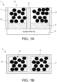
- Figures 1A and 1B depict a portion of a black matrix 1 according to one embodiment of the present disclosure. A black matrix minimizes cross-talk or optical interference between adjacent pixels and provides good display contrast and definition.
- the black matrix 1 includes a plurality or an array of light sources 2 disposed on a substrate 3 with each light source 2 spatially separated from other light sources 2 in the array and a non-transmissive region 4 between the spatially separate light sources 2.
- the light sources 2 may be separated from about 1 ⁇ m to about 1 mm. In another embodiment, the light sources 2 may be separated from about 1 ⁇ m to about 500 ⁇ m. In another embodiment, the light sources 2 may be separated from about 5 ⁇ m to about 300 ⁇ m. In another embodiment, the light sources 2 may be separated from about 10 ⁇ m to about 200 ⁇ m. In another embodiment, the light sources 2 may be separated from about 20 ⁇ m to about 50 ⁇ m.
- the non-transmissive region 4 between the light sources 2 may be from about 1 ⁇ m to about 1 mm. In another embodiment, the non-transmissive region 4 between the light sources 2 may be from about 1 ⁇ m to about 500 ⁇ m. In another embodiment, the non-transmissive region 4 between the light sources 2 may be from about 5 ⁇ m to about 300 ⁇ m. In another embodiment, the non-transmissive region 4 between the light sources 2 may be from about 10 ⁇ m to about 200 ⁇ m. In another embodiment, the non-transmissive region 4 between the light sources 2 may be from about 20 ⁇ m to about 50 ⁇ m.
- a color conversion film 5, as described herein, may be deposited on each of the light sources 2 by printing, such as by ink jet printing.
- the light sources 2 may be light emitting diodes, such as a mini-LED or a micro-LED.
- the color conversion film 5 includes a narrow band emission phosphor 6 dispersed within a matrix 7.
- the non-transmissive region 4 is substantially free of the color conversion film 5 and is substantially non-transmissive to light generated from the plurality of light sources 2.
- the non-transmissive region 4 may be filled by a black matrix material including one or more non-transmissive materials dispersed within a black matrix binder.
- the non-transmissive materials may include, but are not limited to, carbon black powders, dielectric oxides, such as aluminum oxide, or metal particles, such as Ni, Co, Fe, Cr, Cu, Pd, Au, Pt, Sn, Zn and a combination of such.
- the black matrix binder may include binder materials, such as previously described.
- the black matrix binder may be silicone materials, thermoplastic polymers or thermoplastic copolymers.
- the optical density of the non-transmissive region 4, at the wavelength of light corresponding to the emission spectrum of the narrow band emission phosphor 6, is at least 1.0. In another embodiment, the optical density is at least 2.0. In another embodiment, the optical density is at least 3.0. In one embodiment, the non-transmissive region is black or dark.
- the non-transmissive region 4 surrounds each light source 2 or light source 2 with a printed film 5 disposed thereon, as shown in FIG. 1B .
- the black matrix material may be filled to substantially the same height as the height of the light source 2 and color conversion film 5, such that the black matrix has a substantially planar surface, as shown in FIG. 1A .
- the non-transmissive region 4 has a depth of up to about 100 ⁇ m. In another embodiment, the non-transmissive region 4 has a depth from about 1 ⁇ m to about 100 ⁇ m. In another embodiment, the non-transmissive region 4 has a depth from about 10 ⁇ m to about 30 ⁇ m.
- FIG. 2 shows a device 10, according to one embodiment of the present disclosure.
- the device 10 includes a light source 12 and a color conversion film 14.
- the color conversion film 14 is optically coupled or radiationally connected to the light source 12.
- Optically or radiationally coupled or connected means that radiation from the light source 12 is able to excite the phosphor material in the color conversion film 14 and the color conversion film 14 is able to emit light in response to the excitation by the radiation.
- the color conversion film 14 may be disposed on at least a part or portion of the light source 12 or may be located remotely at a distance from the light source 12.
- the light source 12 may be an inorganic LED light source or an organic LED light source.
- ⁇ LED light source' as used herein, is meant to encompass all LED light sources such as semiconductor laser diodes (LD), inorganic light emitting diodes, organic light emitting diodes (OLED) or a hybrid of LED and LD.
- the LED uses a pn-junction diode to emit light when activated through electroluminescence. The color of the light corresponds to the energy of the photon in accordance with the energy band gap of the semiconductor materials.
- the LED light source may be a chip CSP (chip scale package), miniLED, or micro LED, which may be used in self-emissive displays.
- a mini-LED is a sub-millimeter light emitting diode having a size of about 100 ⁇ m to about 0.7 mm.
- the micro-LED has a size smaller than 100 micrometers.
- the micro-LED has a size smaller than 50 micrometers.
- the LED backlight may be miniaturized and arrayed with individual LEDs where each LED element as a pitch is individually addressed and driven to emit light in the same way as self-emitting OLEDs.
- LED light source may be replaced, supplemented or augmented by another radiation source unless otherwise noted and that any reference to semiconductor, semiconductor LED, or LED chip is merely representative of any appropriate radiation source, including, but not limited to, LDs and OLEDs.
- the light source 12 is coated or covered with the color conversion film 14.
- the color conversion coating or film is applied by ink jet printing and coats or covers the light source 12.
- the color conversion film 14 may have multiple layers deposited on the surface of the light source 12.
- the light source 12 may comprise a UV or blue emitting LED. In another embodiment, the light source 12 may include a mini-LED or micro-LED. In some embodiments, the light source 12 produces blue light in a wavelength range from about 440 nm to about 460 nm.
- the device 10 may be a backlight unit for display applications.
- LED backlight units (BLU) for use in displays are based on a combination of a blue LED, such as a mini-LED or micro-LED, and a phosphor material including a green-emitting phosphor and a red-emitting phosphor to provide a white light from the device.
- the green phosphor may be a narrow band green-emitting U 6+ -containing phosphor or a narrow band green-emitting Mn 2+ -containing phosphor.
- the red phosphor includes a narrow band red-emitting phosphor based on complex fluoride materials activated by Mn 4+ .
- the phosphor material includes a combination of a narrow band red-emitting phosphor based on complex fluoride materials activated by Mn 4+ with a narrow band green-emitting U 6+ -containing phosphor or a narrow band green-emitting Mn 2+ -containing phosphor.
- a lighting apparatus comprises the device.
- FIG. 3 illustrates a lighting apparatus or lamp 20, in accordance with some embodiments.
- the lighting apparatus 20 includes a light source 22, such as an LED chip, and leads 24 electrically attached to the light source 22.
- the leads 24 may comprise thin wires supported by a thicker lead frame(s) 26 or the leads 24 may comprise self-supported electrodes and the lead frame may be omitted.
- the leads 24 provide current to light source 22 and thus cause it to emit radiation.
- the LED chip may be a mini-LED chip or a micro-LED chip.
- the light source 22 may be encapsulated within an envelope 28.
- the envelope 28 may be formed of, for example, glass or plastic.
- the light source 22 may be enclosed by an encapsulant material 32.
- the encapsulant material 32 may be a low temperature glass, or a polymer or resin known in the art, for example, an epoxy, silicone, epoxy-silicone, acrylate or a combination thereof.
- the lighting apparatus 20 may only include the encapsulant material 32 without the envelope 28. Both the envelope 28 and the encapsulant material 32 should be transparent to allow light to be transmitted through those elements.
- a color conversion film 34 is disposed on a light emitting surface of the light source 22.
- the film 34 may be disposed by any appropriate method, for example, by coating or printing.
- the layer 34 may be disposed for example, coated over or directly on the surface of the light source 22 by coating or printing and drying or curing the coating over the LED light source 22.
- the light emitted by the light source 22 mixes with the light emitted by the color conversion film 34 to produce desired emission.
- a color conversion film 38 is coated onto a surface of the envelope 28 as illustrated in FIG. 4 showing an exemplary embodiment of a lighting apparatus 40, instead of being formed over the light source 22 ( FIG. 3 ).
- the film 38 is coated on an inside surface 29 of the envelope 28, although the film 38 may be coated on an outside surface of the envelope 28, if desired.
- the film 38 may be coated on the entire surface of the envelope 28 or only a top portion of the inside surface 29 of the envelope 28.
- the light emitted by the light source 22 mixes with the light emitted by the film 38, and the mixed light transmits out.
- the color conversion film may be located in either or both locations (as shown in Figures 3 and 4 ) or in any other suitable location, such as in a remote location, separately from the envelope 28 or integrated into the light source 22.
- the lighting apparatus 20 or 40 shown respectively in FIG. 3 or FIG. 4 may also include a plurality of scattering particles (not shown), which are embedded in the encapsulant material 32.
- the scattering particles may comprise, for example, alumina, silica, zirconia, or titania. The scattering particles effectively scatter the directional light emitted from the light source 22, preferably with a negligible amount of absorption.
- the lighting apparatus 20 or 40 shown in FIG. 3 or FIG. 4 may be a backlight apparatus.
- the backlight apparatus comprises a backlight unit 10.
- Some embodiments are directed to a backlight apparatus 50 as illustrated in FIG. 5 .
- the backlight apparatus 50 includes a surface mounted device (SMD) type light emitting diode for backlight or display applications.
- SMD surface mounted device
- This SMD is a "side-emitting type" and has a light-emitting window 52 on a protruding portion of a light guiding member 54.
- An SMD package may comprise an LED chip and a color conversion film.
- the backlight apparatus may be an edge lit apparatus or side-emitting apparatus.
- the backlight apparatus may be a direct lit apparatus.
- a backlight apparatus and related devices are described in U.S. Publication No. 2017/0254943 and PCT Publication No. 2018/190827 , the entire contents of each of which are incorporated herein by reference.
- FIG. 6A illustrates an embodiment of a single mode liquid crystal display (LCD) with an edge lit backlight configuration.
- LCD 100A includes a light apparatus or backlight apparatus 102, as described previously in FIG. 3 or FIG. 4 , light guide panel 106 and an LCD panel 120.
- the LCD 100A uses the LCD panel 120 with control electronics and the backlight apparatus 102 to produce color images.
- the backlight apparatus 102 provides white light and represents a plurality of backlight apparatuses 102 along one or more edges of the LCD 100A.
- the LCD 100A uses the LCD panel 120 with control electronics and the LED backlighting 100 to produce color images.
- the LCD panel 120 includes color filters 122 arranged in subpixels, such as a red color filter, a green color filter and a blue color filter.
- the red, green and blue filters 122 transmit a light having a specific wavelength of white light incident from the backlight apparatus 102.
- the filters 122 transmit wavelengths of light corresponding to the color of each filter and absorb other wavelengths.
- the LCD panel 120 may include a front polarizer 118, a rear polarizer 114, a thin film transistor (TFT) 126 and liquid crystal 116, as well as electrodes (not shown).
- the color filters 122 may be positioned between the liquid crystal 116 and the front polarizer 118.
- the thin film transistor 126 may be positioned between the liquid crystal 116 and the rear polarizer 114.
- Each pixel has a corresponding transistor or switch for controlling voltage applied to the liquid crystal 116.
- the front and rear polarizers 118 and 114 may be set at right angles.
- the LCD panel 120 is opaque.
- rod-shaped polymers align with the electric field and untwist such that the voltage controls the light output from the front polarizer 118.
- the liquid crystal 116 rotates so that there is a light output from the front polarizer 118.
- White light from the backlight apparatus 102 travels toward light guide panel (LGP) 106, through diffuser film 110 and prism 108, as well as double brightness enhanced film (DBEF) 124, which provides a uniform light backlight for the LCD panel 120.
- LGP light guide panel
- DBEF double brightness enhanced film
- the LED backlighting 102 and LCD 100A may include additional components typical in an optical stack.
- diffusers, reflectors or glass filters may be provided.
- a cover glass may cover the optical stack.
- FIG. 6B illustrates an embodiment of a single mode LCD 100B with a direct view/lit backlight configuration.
- the direct lit backlight configuration is similar to the edge lit backlight configuration shown in FIG. 6A , except that there is no light guide panel 106 and there is a different arrangement of LEDs.
- a plurality of backlight apparatuses 102 are arranged to directly provide light to a diffuser plate 128, which may support a diffuser film 110.
- FIG. 7 illustrates an exemplary embodiment of a backlight unit or module 200 that includes light source 12 as previously described in FIG. 2 , light guide panel (LGP) 204, color conversion film 206, dichroic filter 210 and LCD panel 120 as previously described in FIG. 6A .
- Backlight unit 200 may also optionally include a prism 212 and a double brightness enhanced film (DBEF) 214.
- the light source 12 is a blue emitting LED and may be a mini-LED or micro-LED. To produce even lighting, blue light from the light source 12 first passes through light guide panel 204, which diffuses the blue light. Generally, there is an air space between the LCD panel 120 and the double brightness enhanced film (DBEF) 214.
- the double brightness enhanced film is a reflective polarizer film which increases efficiency by repeatedly reflecting any unpolarized light back, which would otherwise be absorbed by the LCD's rear polarizer 118.
- the double brightness enhanced film 214 is placed behind the LCD panel 120 without any other film in-between.
- the double brightness enhanced film 214 may be mounted with its transmission axis substantially parallel to the transmission axis of the rear polarizer 118.
- the double brightness enhanced film 214 helps recycle the white light 220 that would normally be absorbed by the rear polarizer 118 of the LCD panel 120, and thus, increases the brightness of the LCD panel 120 and light 222 emitting from the LCD panel 120.
- the prism 212 may be removed or substituted by other brightness enhancement components.
- the double brightness enhanced film may be removed.
- the backlight unit or module 200 includes a color conversion film 206 located remotely at a distance from the light source 12.
- the color conversion film 206 includes phosphor material including particles of a narrow band emission phosphor.
- the phosphor material includes a green-emitting phosphor 208A and a red-emitting phosphor 208B.
- the green-emitting phosphor comprises a narrow band green-emitting U 6+ -containing phosphor or a narrow band green-emitting Mn 2+ -containing phosphor.
- the red-emitting phosphor comprises a narrow band red-emitting phosphor based on complex fluoride materials activated by Mn 4+ .
- the color conversion film 206 is remote in the sense that the primary light source and the phosphor material are separate elements, and the phosphor material is not integrated with the primary light source as a single element. Primary light is emitted from the primary light source and travels through one or more external media to radiationally or optically couple the light source 12 to the phosphor material in the color conversion film 206.
- a backlight unit or module may vary in configuration.
- a direct lit configuration may be used, similar to the direct light configuration shown in FIG. 6B .
- a display device or display provides information or images from a processor or other type of information management system by converting electrical signals into pixilated multicolor displays.
- Displays may be self-emissive, such as micro-LED or organic light emitting diode displays (OLED) with organic light emitting diode layers to produce light.
- a liquid crystal display (LCD) uses backlighting, such as from LED light sources and individual liquid crystal cells.
- the display device includes the color conversion film as previously described. Examples of devices that include a backlighting or direct emission display.
- Display applications include, but are not limited to televisions, plasma screens, home and theater projections, digital photo frames, tablets, automotive displays, e-book reader, electronic dictionary, digital camera, computers, laptops, computer monitors, electronic keyboard, cellular or conventional phone, mobile phones, smartphones, tablet computers, gaming device, other handheld devices that have a display and other electronic devices with a screen.
- the list of these applications is meant to be merely exemplary and not exhaustive.
- T/BEA A mixture of solvents, referred to as T/BEA, was prepared by mixing 33.2g of terpineol with 16.6g 2-(2-Butoxyethoxy)ethyl acetate (BEA) at room temperature and stirred for 30mins.
- PFS Sample Nos. 395 and F2531-120-2 Two phosphor PFS (K 2 SiF 6 :Mn 4+ ) powders, PFS Sample Nos. 395 and F2531-120-2 were used in this Example.
- PFS Sample No. F2531-120-2 has a D10/D50/D90 particle size distribution of 8.9/10.5/12.3 ⁇ m.
- PFS Sample No. 395 was prepared by the process described in US Publication No. 2018/0163126 .
- the powder was washed in a nearly saturated solution of K 2 SiF 6 in 49%HF and annealed at 540°C for 8 hours under a 20% fluorine:80% nitrogen atmosphere.
- the annealed powder was sifted through 280 mesh.
- the powder was sonicated to a D50 particle size of 7.9 ⁇ m with a D10/D50/D90 particle size distribution of 6.9/7.9/9.2 ⁇ m, as measured by Horiba Particle Size Analyzer.
- PFS Sample No. F2531-120-2 was prepared from PFS Sample No. 425 (K 2 SiF 6 :Mn 4+ ) by surface coating the PFS powder with 2.5% MgF 2 .
- PFS Sample No. 425 was prepared by the process described in US Publication No. 2018/0163126 . The powder was washed in a nearly saturated solution of K 2 SiF 6 in 49%HF and annealed at 540°C for 8 hours under a 20% fluorine: 80% nitrogen atmosphere. The annealed powder was sifted through 280 mesh and washed in a second wash treatment step in a nearly saturated solution of K 2 SiF 6 in 49%HF for 30 minutes.
- PFS sample has a D50 particle size of 12.0 ⁇ m (unsonicated).
- the powder was coated with MgF 2 , as follows: 12 mL of a 0.22 g/mL solution of MgSiF 6 ⁇ 6H 2 O in 17.5% aq. H 2 SiF 6 was added over 30 minutes into a reaction mixture containing a magnetic stir bar and 25 g of K 2 SiF 6 :Mn 4+ in 240 mL of 49% aq HF saturated with K 2 SiF 6 . The mixture was stirred vigorously for 30 sec (300 rpm) after which the stirring was turned down to 120 rpm. After the addition was complete, the stirring was stopped, the stir bar was removed and the reaction mixture was allowed to settle for 5 minutes. The supernatant was decanted and discarded.
- the wet slurry was mixed with 150 mL of 49% aq HF saturated with K 2 SiF 6 .
- the wash mixture was allowed to settle for 5 minutes and then the supernatant was decanted and discarded.
- the slurry was transferred to a plastic Buchner funnel fitted with a 0.65 ⁇ m fluoropolymer membrane.
- the residual HF solution was filtered off and the phosphor cake was washed with acetone 5 times, using a total of 500 mL acetone, churning the solid before each wash.
- EC-L ethyl cellulose
- EC-M ethyl cellulose
- EC-H ethyl cellulose
- EC-HH ethyl cellulose
- a 3.3 wt% solution of EC-M was prepared by mixing 0.35 g of EC-M (see Example 1) in 10.25 g of T/BEA solvent mixture (see Example 1), hereafter referred to as T/BEA_EC-M(3.3%).
- a 3.3 wt% solution of EC-H was prepared by mixing 0.42 g of EC-H (see Example 1) in 12.3 g of T/BEA solvent mixture hereafter referred to as T/BEA_EC-H(3.3%). The two solutions were stirred overnight at 80°C to dissolve the ethyl cellulose completely, and then cooled to room temperature for the following experiments.
- PFS Sample No. F2531-120-2 (see Example 1) was mixed with 3g of T/BEA_EC-M(3.3%) varnish to prepare a PFS-containing dispersion, referred to as T/BEA_EC-M(3.3%)-PFS(5%); 0.19g of PFS Sample No. F2531-120-2 was mixed with 3.8g of T/BEA_EC-H(3.3%) varnish to prepare a PFS-containing dispersion, referred to as T/BEA_EC-H(3.3%)-PFS(5%); 0.2651g of PFS Sample No.
- All of the dispersions having a PFS loading of 5wt% were first stirred for 2 hours at room temperature, followed by vigorous mixing on a vortex mixer for 1-2 minutes to reduce the particle agglomerates, and rolled at a speed of 60 rpm on a bottle roller for 2 hours.
- the homogeneous dispersions were stirred for another 2 hours at 80°C and then cooled down to room temperature for settling tests. Dry films coated from the dispersions had a PFS to binder (EC) ratio of 60 to 40.
- Sample T/BEA_EC-M(3.3%)-PFS395(5%) had some settling; and Sample T/BEA_EC-H(3.3%)-PFS395(5%) had no settling.
- Sample T/BEA_EC-M(3.3%)-PFS(5%) had some settling; and Sample T/BEA_EC-H(3.3%)-PFS(5%) had no settling.
- Sample T/BEA_EC-M(3.3%)-PFS395(5%) had increased settling; and Sample T/BEA_EC-H(3.3%)-PFS395(5%) had minimal settling.
- Sample T/BEA_EC-M(3.3%)-PFS(5%) had increased settling; and Sample T/BEA_EC-H(3.3%)-PFS(5%) had no settling.
- the two dispersions were first stirred for 2 hours at room temperature, followed by vigorous mixing on a vortex mixer for 1-2 minutes to reduce the particle agglomerates, and rolled at a speed of 60 rpm on a bottle roller for 2 hours.
- the homogeneous dispersions were stirred for another 2 hours at 80 °C, and then cooled down to room temperature for settling tests.
- Sample T/BEA_EC-M(3.3%)-PFS(40%) had about 30% settling; and Sample T/BEA_EC-H3.3%)-PFS(40%) had about 25% settling.
- Sample T/BEA_EC-M(3.3%)-PFS(40%) had about 50% settling; and Sample T/BEA_EC-H3.3%)-PFS(40%) had about 30% settling.
- T/BEA_EC-H3.3%)-PFS(40%) dispersion has better dispersion stability than T/BEA_EC-M(3.3%)-PFS(40%) due to its higher viscosity.
- Table 2 Shown in Table 2 are results for spin-coated films using the dispersion of T/BEA_EC-H(3.3%)-PFS(40%).
- the final dry films consist of ⁇ 92% of PFS and -8% EC-H.
- the films are free of uniformity defects.
- Table 2 Spin speed (krpm) Film thickness (um) Blue-to-red conversion efficiency 0.7 33 36.7% 1.2 25 36.3% 4 12 26.3%
- PVDF-HFP poly(vinylidene fluoride-co-hexafluoropropylene)
- CH cyclohexanone
- the solution referred to as CH_PVDF-HFP has a viscosity of 15.37cP at 25°C, which translates to a sedimentation velocity of less than 1mm/hr for a 2 ⁇ m K 2 SiF 6 :Mn 4+ particle.
- PFS Sample No. F2664-43-1 was prepared from PFS Sample No. 466 (K 2 SiF 6 :Mn 4+ ) by surface coating the PFS powder with 2.5% MgF 2 .
- PFS Sample No. 466 was prepared by the process described in US Publication No. 2018/0163126 . The powder was washed in a nearly saturated solution of K 2 SiF 6 in 49%HF and annealed at 540°C for 8 hours under a 20% fluorine:80% nitrogen atmosphere. The annealed powder was sifted through 280 mesh.
- the PFS sample has a D50 particle size of 9.96 ⁇ m without sonication and 9.4 ⁇ m under sonication.
- the powder was coated with MgF 2 , as follows: 35.48 mL of a 0.22 g/mL solution of MgSiF 6 ⁇ 6H 2 O in 17.5% aq. H 2 SiF 6 was added over 30 minutes into a reaction mixture containing a magnetic stir bar and 70g of K 2 SiF 6 :Mn 4+ in 665 mL of 49% aq HF saturated with K 2 SiF 6 .
- the mixture was stirred vigorously for 30 sec (300 rpm) after which the stirring was turned down to 120 rpm. After the addition was complete, the stirring was stopped, the stir bar was removed and the reaction mixture was allowed to settle for 5 minutes. The supernatant was decanted and discarded.
- the wet slurry was mixed with 250 mL of 49% aq HF saturated with K 2 SiF 6 .
- the wash mixture was allowed to settle for 5 minutes and then the supernatant was decanted and discarded.
- the slurry was transferred to a plastic Buchner funnel fitted with a 0.65 ⁇ m fluoropolymer membrane.
- the residual HF solution was filtered off and the phosphor cake was washed with acetone 5 times, using a total of 1 L acetone, churning the solid before each wash.
- PFS Sample No. F2664-43-1 was mixed with 3.45g of CH_PVDF-HFP varnish to prepare a 40wt% PFS dispersion, referred to as CH_PVDF-HFP-PFS(40%).
- the dispersion was first stirred for 2 hours at room temperature, followed by vigorous mixing on a vortex mixer for 1-2 minutes to reduce the particle agglomerates, and rolled at a speed of 60-70 rpm on a bottle roller for 2 hours.
- the homogeneous dispersion was stirred for another 2 hours at 80°C, and then cooled down to room temperature for film coating.
- the dispersion having PVDF-HFP was very stable and shows little sedimentation after 30mins.
- the majority of PFS particles in a dispersion in cyclohexanone without PVDF-HFP settle to the bottom within 10 minutes.
- the dispersion CH_PVDF-HFP-PFS(40%) was then used to spin-coat PFS:PVDF-HFP films.
- Pre-cleaned glass slides were used as substrates for spin coating that was carried out in air.
- Approximately 0.7 ml mixture was added onto the substrate, which was then spun at 700 rpm for 20 seconds to spread the liquid and then (without stopping) at 1500 rpm for 60 seconds to obtain a wet film.
- the wet film was baked on a pre-heated hotplate at 150°C for 10 mins before testing.
- the final baked film consisting of 97.4% of PFS in 2.6% PVDF-HFP has a thickness of ⁇ 35 ⁇ m and a blue-to-red conversion efficiency of 36.8%.
- PFS Sample No. 395 Two samples were prepared using PFS Sample No. 395 (see Example 1).
- a binder material poly(methyl acrylate) (PMA) 40wt% solution in toluene was purchased from Aldrich with a product number of 182214 and M w of ⁇ 40,000 and used as received.
- PMA poly(methyl acrylate)
- PFS-PMA-Toluene 1g of PFS Sample No.
- PFS Sample No. 320 which is PFS (K 2 SiF 6 :Mn 4+ ) having a D10/D50/D90 particle size distribution of 9.0/13.6/20.2 ⁇ m.
- a binder material polyvinyl alcohol (PVA) was purchased from Aldrich with a product number of 363065 and M w of 146,000-186,000 and used as received.
- PFS Sample No. 320 was prepared by the process described in US Publication No. 2018/0163126 .
- the powder was washed in a nearly saturated solution of K 2 SiF 6 in 49%HF and annealed at 540°C for 8 hours under a 20% fluorine:80% nitrogen atmosphere.
- the annealed powder was sifted through 280 mesh and washed in a second wash treatment step in a nearly saturated solution of K 2 SiF 6 in 49%HF for 30 minutes.
- the powder was subjected to a 'roasting' step, an additional low temperature anneal performed after the second wash treatment, at 150°C for four hours under a 20% fluorine:80% nitrogen atmosphere.
- the powder had a D50 particle size of 13.6 ⁇ m, as measured by SEM.
- the powder has Mn% of about 1.32.
- Sample No. 320 was dispersed into 2 ml of 2,2,3,3-tetrafluoro-1-propanol (TFPO).
- TFPO 2,2,3,3-tetrafluoro-1-propanol
- 5D 0.5g of the Sample No. 320 and 0.03g of PVA were dispersed into 2 ml of TFPO and mixed well. Both samples were vortexed for 30 seconds to form dispersions and then left undisturbed to observe settling behavior.
- T/BEA_PVB binder material polyvinyl butyral
- PFS Sample No. PFS GRC082718SSTGA(316/318) was used.
- the PFS Sample K 2 SiF 6 :Mn 4+ (PFS) was prepared by the process described in US Publication No. 2018/0163126 .
- the powder was washed in a nearly saturated solution of K 2 SiF 6 in 49%HF and annealed at 540°C for 8 hours under a 20% fluorine:80% nitrogen atmosphere.
- the annealed powder was sifted through 280 mesh and washed in a second wash treatment step in a nearly saturated solution of K 2 SiF 6 in 49%HF for 30 minutes.
- the powder had a D10/D50/D90 particle size distribution of 9.8/14.4/21.8 ⁇ m.
- Another film was prepared using Sylgard 184 diluted with toluene.
- 2g of Sylgard 184 Part A was diluted with 1g toluene and mixed well.
- 0.5g of Sylgard 184 part B was diluted with 0.25g toluene and mixed well.
- 0.73g of Sample No. 316/318 was mixed with the diluted Sylgard 184 A+B and the mixture was gently mixed with a wooden stick to obtain a homogenous dispersion.
- the mixture was degassed under a vacuum for 5 min. Pre-cleaned glass slides were used as substrates for spin coating that was carried out in air. First, approximately 0.5ml of the mixture was applied onto the substrate and spun at 500 rpm for 15 seconds and then (without stopping) spun at 3000 rpm for 60 seconds to obtain a wet film. The coated substrate was baked on a pre-heated hotplate for 30 seconds to dry off any volatile materials. The coated substrate was placed in a pre-heated oven and the film was cured at 125°C for 30 min. The thickness of the resulting film was about 35 ⁇ m. The film had a blue-to-red conversion efficiency of 41.7%.
- a stock solution of a photo-initiator Igracure ® 819 was prepared by dissolving 80 mg of Irgacure ® 819 with 1 ml of 2,2,3,3-tetrafluoro-1-propanol (TFPO).
- TFPO 2,2,3,3-tetrafluoro-1-propanol
- PFS Sample No. F2531-120-2 (see Example 1) was mixed with 1.63g binder material ethoxylated trimethylolpropane triacrylate (Tradename, SR454 obtained from Sartomer Americas) to obtain a dispersion with 40wt% PFS loading. The dispersion was then mixed with 0.20 ml of the Irgacure ® 819 stock solution in TFPO to obtain a 40wt% PFS dispersion, referred to as SR454-PFS-Dispersion-1.
- binder material ethoxylated trimethylolpropane triacrylate (Tradename, SR454 obtained from Sartomer Americas)
- the two dispersions were first stirred for 2 hours at room temperature, followed by vigorous mixing on a vortex mixer for 1-2 minutes to reduce the particle agglomerates, and rolled at a speed of 60-70 rpm on a bottle roller for 2 hours.
- the homogeneous dispersions were stirred for another two hours at 50°C, and then cooled to room temperature.
- Pre-cleaned glass slides were used as substrates for spin coating that was carried out in air. After spin-coating, the substrates with PFS coating were baked on a hotplate pre-heated to 110°C for 10mins before UV-curing under a UV intensity of 39 mW/cm 2 in air. The final films were about 50 ⁇ m thick and consisted of -40% PFS in the crosslinked acrylate matrix. The spin-coated films of both samples had good blue-to-red conversion efficiency of 44% and were stable under UV radiation.
- PFS:photoresist films were prepared by spin-coating a single layer of the corresponding liquid formulations directly on pre-cleaned glass and Silicon wafer substrates. However, none of the mixtures provided desirable uniform coatings.
- Bilayer Structures were constructed.
- a layer of a photoresist material (A) free of phosphor was coated onto a substrate, which may be glass or a Silicon wafer.
- a layer of a photoresist material (B) was mixed with 10wt% PFS and coated onto the substrate over the photoresist A coating. Coverage and uniformity of the films is shown in Table 3.
- T/BEA a primary solvent
- terpineol a primary solvent
- BEA 2-(2-Butoxyethoxy)ethyl acetate
- T/BEA a co-solvent
- the mixture was stirred at room temperature for 30 min.
- 0.3088g of binder material ethyl cellulose (EC-H) was mixed with 9.98g of the T/BEA solvent mixture to prepare a 3 wt% solution of ethyl cellulose (EC-H), referred to as T/BEA_EC-H(3%).
- T/BEA_EC-H(3%) a 3 wt% solution of ethyl cellulose
- the solution was stirred overnight at 80°C to dissolve the EC-H completely and then cooled to room temperature.
- T/BEA_EC-H(3%)-PFS(10%) 0.3355g of PFS Sample No. F2531-120-2 (see Example 1) was mixed with 3.1g of the T/BEA_EC-H(3%) varnish to form a 10wt% PFS dispersion, referred to as T/BEA_EC-H(3%)-PFS(10%).
- T/DGME a primary solvent
- terpineol a primary solvent
- DPE Diethylene glycol methyl ether
- T/DGME a co-solvent
- EC-H binder material ethyl cellulose
- T/DGME_EC-H(3%) a 3 wt% solution of ethyl cellulose
- the solution was stirred overnight at 80°C to dissolve the EC-H completely and then cooled to room temperature.
- 0.4632g of PFS Sample No. F2531-120-2 was mixed with 4.2g of the T/DGME_EC-H(3%) varnish to form a 10wt% PFS dispersion, referred to as T/DGME_EC-H(3%)-PFS(10%).
- Both dispersions were stirred for 2 hours at room temperature, followed by vigorous mixing on a vortex mixer for 1-2 minutes to reduce the particle agglomerates, and rolled at a speed of 60 rpm on a bottle roller for 2 hours.
- the homogeneous dispersions were stirred for another 2 hours at 80°C, and then cooled to room temperature for settling tests.
- varying co-solvent is one of the methods of adjusting ink rheological properties such as viscosity, which subsequently affects ink stability and sedimentation speed.
- Table 4 Dispersion Co-solvent Binder Varnish Viscosity (cP, 25 °C) Calculated Sedimentation speed (mm/hr) T/DGME_EC-H(3%)-PFS(10%) DGME EC-H 302.1 0.3 T/BEA_EC-H(3%)-PFS(10%) BEA EC-H 258 0.4
- PFS Sample No. F2531-120-2 containing dispersions were prepared in the same way as disclosed in Example 1: T/BEA_PVP(3%)-PFS(10%), T/BEA_EC-HH(3%)-PFS(10%) and T/BEA_PEI(3%)-PFS(10%).
- T/BEA_PVP(3%) A 3 wt% of PVP solution, referred to as T/BEA_PVP(3%), was prepared by mixing 0.29 g of PVP with 9.4 g of the T/BEA solvent mixture.
- T/BEA_EC-HH(3%) A 3 wt% of EC-HH solution, referred to as T/BEA_EC-HH(3%), was prepared by mixing 0.766 g of EC-HH with 24.78 g of the T/BEA solvent mixture.
- T/BEA_PEI(3%) A 3 wt% of PEI solution, referred to as T/BEA_PEI(3%), was prepared by mixing 0.32 g of PEI in 10.6 g of T/BEA solvent mixture.
- All dispersions were first stirred for 2 hours at room temperature, followed by vigorous mixing on a vortex mixer for 1-2 minutes to reduce the particle agglomerates, and then rolled at a speed of 60 rpm on a bottle roller for 2 hours. The homogeneous dispersions were stirred for another 2 hours at 80°C, and cooled down to room temperature for settling tests.
- Sample T/BEA_PVP(3%)-PFS(10%) had about 10% settling
- Sample T/BEA_EC-HH(3%)-PFS(10%) had no settling
- Sample T/BEA_PEI(3%)-PFS(10%) had about 70% settling.
- Sample T/BEA_PVP(3%)-PFS(10%) had about 10% settling
- Sample T/BEA_EC-HH(3%)-PFS(10%) had no settling
- Sample T/BEA_PEI(3%)-PFS(10%) had about 80% settling.
- Sample T/BEA_PVP(3%)-PFS(10%) had about 50% settling
- Sample T/BEA_EC-HH(3%)-PFS(10%) had about 15% settling
- Sample T/BEA_PEI(3%)-PFS(10%) had settled.
- varying binder materials is another effective approach of adjusting ink rheological properties such as viscosity, which subsequently affects ink stability and sedimentation speed.
- Table 5 Dispersion Co-solvent Binder Varnish Viscosity (cP, 25 °C) Calculated Sedimentation speed (mm/hr) T/BEA_PVP(3%)-PFS(10%) BEA PVP 210.7 0.5 T/BEA_EC-HH(3%)-PFS(10%) BEA EC-HH 878.3 0.1 T/BEA_PEI(3%)-PFS(10%) BEA PEI 11.15 8.4
- a dried 20 ml vial equipped with a stir bar was charged with 2-butanol (8.26 g), water (0.203 g, 11.3 mmol), and isobutyric acid (0.2933 g, 2.8 mmol) at room temperature. After the mixture was stirred for approximately 15 min, tantalum ethoxide (0.844 g, 2.1 mmol) was added to the stirred solution dropwise. The homogeneous solution was allowed to stir at room temperature for 22 hours to provide a solution of 2 nm Ta 2 O 5 nanoparticles.
- the Ta 2 O 5 nanoparticles solution was mixed with 6.19 g of T/BEA varnish with 3 wt% EC-H binder material in a flask, and then the 2-butanol was stripped from the homogeneous solution using rotoevaporation.
- the remaining solution referred to as T/BEA_EC-H_Ta 2 O 5 is optically clear and has a viscosity of 249.9 cP at 25°C.
- the solution has 6.9wt% Ta 2 O 5 and 3.0wt% of binder (or in another word, the solid binder composite consists of 70% of Ta 2 O 5 and 30% binder).
- the solution has an effective refractive index of 1.62 (Table 18).
- Adjusting the content of metal oxide dispersed in the binder (Example 1 in Table 6) or replacing Ta 2 O 5 with other metal oxides such as ZrO 2 and TiO 2 having lower densities (Examples 2 in Table 6) can further optimize the effective refractive index of the binder material to achieve optimum performance.
- a dried 250 ml flask equipped with a stir bar was charged with isopropanol (IPA) (90 ml), water (1.16 g, 64.4 mmol), and isobutyric acid (IBA) (1.7 g, 16.2 mmol) at room temperature. After the mixture was stirred for 30 min, tantalum ethoxide (5.8 g, 14.4 mmol) was added to the stirred solution dropwise. The homogeneous solution was allowed to stir at room temperature for 21 hours to provide a solution of 2.2 nm Ta 2 O 5 nanoparticles.
- IPA isopropanol
- IBA isobutyric acid
- the Ta 2 O 5 nanoparticles solution was mixed with 3.15g binder material ethoxylated trimethylolpropane triacrylate (Tradename SR454) in a flask. Isopropanol was stripped from the clear solution using rotary evaporation. The low boiling point solvents (IPA/H 2 O/IBA) were further stripped off using nitrogen blowing. The final clear solution (11.6 g) contained 3.15g of acrylate and 3.15-3.18g of Ta 2 O 5 nanoparticles. The weight percentage of solid content is 1 part of acrylate to 1 part of Ta 2 O 5 in the final solution.
- binder material ethoxylated trimethylolpropane triacrylate (Tradename SR454) in a flask. Isopropanol was stripped from the clear solution using rotary evaporation. The low boiling point solvents (IPA/H 2 O/IBA) were further stripped off using nitrogen blowing. The final clear solution (11.6 g) contained 3.15g of acryl
- Sample F2664-5-8 crystallized on cooling to give a hard paste-like consistency, so it was diluted with an additional 4g PGMEA and heated until homogeneous again. Upon cooling the second time a less crystalline stable opaque dispersion formed.
- 0.1g functionalized wax sample 2280-121 (dodecyl cinnamide) was dissolved in 2g each of ethylene glycol phenyl ether methacrylate (1.85 mL, Sample No. F2664-5-17), polypropylene glycol dimethacrylate (1.98 mL, Sample No. F2664-5-18), and triethylene glycol dimethacrylate (1.83 mL, Sample No. F2664-5-19). Each sample was heated until homogeneous and allowed to cool undisturbed. Sample Nos. F2664-5-18 and F2664-5-19 remained homogeneous on cooling while Sample No. F2664-5-17 formed an opaque thick dispersion. 0.5g of PFS Sample No.
- Sample No. F2664-5-17 was added to Sample No. F2664-5-17.
- a separate sample (Sample No. F2664-5-20) of 0.5g PFS Sample No. 395 and 2g of ethylene glycol phenyl ether methacrylate was prepared.
- Sample No. F2664-5-17 was heated to dissolve the wax and Sample Nos. F2664-5-17 and F2664-5-20 were vortexed to mix thoroughly and allowed to cool undisturbed.
- PFS Sample No. 395 was dispersed in isopropanol (IPA) to prepare the A-series samples (10wt% PFS) with and without dispersants (Table 9).
- Table 9 Sample PFS Sample No. 395 IPA Dispersant Dispersant/PFS (wt%) A-1 0.804 g 7.24 g TEGO 655 20% A-2 0.514 g 4.63 g TEGO 685 20% A-3 0.67 g 6.03 g TEGO 687 20% A-4 0.61 g 5.49 g TEGO 689 20% A-5 0.59 g 5.31 g TEGO 690 20% A-6 0.78 g 7.02 g 0
- All the dispersions were first stirred for two hours at room temperature, followed by vigorous mixing on a vortex mixer for 1-2 minutes to reduce the particle agglomerates, and rolled at a speed of 60-70 rpm on a bottle roller for 2 hours.
- the homogeneous dispersion was stirred for another two hours at 80°C, and cooled to room temperature for settling tests.
- PFS Sample No. 40C180101-01ATS was prepared by the process described in US Publication No. 2018/0163126 .
- the powder was washed in a nearly saturated solution of K 2 SiF 6 in 49%HF and annealed at 540°C for 8 hours under a 20% fluorine:80% nitrogen atmosphere.
- the annealed powder was sifted through 280 mesh.
- the powder had a D50 particle size of 26.1 ⁇ m, as measured by SEM.
- the powder has Mn% content of about 1.58%.
- PFS Sample No. 40C180101-01ATS was surface coated with MgF 2 in varying amounts as shown in Table 11.
- a representative procedure for coating the phosphor was: 100 mL of a 0.22 g/mL solution of MgSiF 6 ⁇ 6H 2 O in 17.5% aq. H 2 SiF 6 was added over 30 minutes into a reaction mixture containing a magnetic stir bar and 50g of K 2 SiF 6 :Mn 4+ in 400 mL of 49% aq HF saturated with K 2 SiF 6 .
- the mixture was stirred vigorously for 30 sec (300 rpm) after which the stirring was turned down to 120 rpm. After the addition was complete, the stirring was stopped, the stir bar was removed and the reaction mixture was allowed to settle for 5 minutes.
- the Zeta potentials were measured in ethanol using folded capillary cells.
- PFS having higher MgF 2 coating weight tended to have increased zeta potential.
- the addition of a MgF 2 surface coating is also evidenced by the decreased QE degradation after testing at 85°C and 85% RH for 200 hrs and increased particle stability.
- Comparative-1 0.78g of PFS (sample ID 040-1700501) was added into a pre-mixed Sylgard TM 184A (2.10g) and Sylgard TM 184B (0.21g) blend. The mixture was mixed well using a narrow wood stick to obtain a homogeneous blend, which was then degassed using house vacuum for 30 mins to remove air bubbles. 0.70g of the mixture was manually poured on a template to create a circular tape with diameter of 2.87cm and then cured at 90°C for 30 min. The thickness of 793 ⁇ m was measured using a digital caliper.
- each mixture was mixed well using a narrow wood stick to obtain a homogeneous blend, which was then degassed using house vacuum for 30 min to remove air bubbles.
- Approximately 1.0 ml of each mixture was applied to a 2"x3" pre-cleaned glass slide and processed by the doctor blade using a 127 ⁇ m gap to generate a 127 ⁇ m thick wet film, which was cured at 90°C for 30 minutes to obtain a dry film having a thickness of 127 ⁇ m.
- Haze measurements were performed using a home-made Hazemeter.
- the Hazemeter consisted of an eight-inch integration sphere and a collimated LED light source.
- the film sample was placed at the entrance port of the integration sphere.
- Each measurement measures two transmission values at 450 nm with the exit port either covered with a cap [total transmission denoted as T% (total)] or without the cover cap [diffuse transmission denoted as T% (diffuse)].
- the haze value is the ratio of T% (diffuse) divided by T% (total).
- haze of PFS containing films may be optimized by varying Mn%, particle size and scattering strength by controlling the refractive index of the matrix.
- the amount of activator Mn incorporation in phosphors (referred to as Mn%) has a significant effect on color conversion. Shown in Table 13 are color conversion features of films of PFS (25wt%) dispersed in silicone illuminated by a blue LED. Increasing the degree of Mn% incorporation in PFS reduces the bleed-through of blue light and increases the intensity of red emission. Table 13 PFS name Mn% incorporation Bleed through of blue light Ratio of peak intensity (I631nm/I440nm) PFS-1 0.7% 44% 2.8 F2531-122-25 1.4% 21% 8.9 F2664-26-3 2.1% 15% 13.3 GRC022520BTGA(470) 3.1% 7% 32.6
- T/BEA_PVPS(3%) Poly(vinyl phenyl sulfide) (PVPS) having a refractive index of 1.657 (purchased from Aldrich (product number 640212) was used as received) was mixed with 8.7 g of T/BEA (see Example 1), referred to as T/BEA_PVPS(3%), and stirred overnight at 80°C to obtain a clear solution.
- PFS Sample No. F2664-43-1 (see Example 4) was mixed with 2.16 g of T/BEA_PVPS varnish to obtain a suspension having a PFS concentration of 40wt%, referred to as T/BEA PVPS-PFS (40%).
- the suspension was first stirred for 2 hours at room temperature, followed by vigorous mixing on a vortex mixer for about two minutes to reduce the particle agglomerates and rolled at a speed of 60-70 rpm on a bottle roller for 2 hours.
- the homogeneous suspension was stirred for another 2 hours at 80°C and cooled to room temperature for film coating.
- the T/BEA_PVPS-PFS(40%) suspension was then used to spin-coat PFS:PVPS films.
- Pre-cleaned glass slides were used as substrates for spin coating that was carried out in air.
- Approximately 0.5ml of the suspension was added onto the substrate and spun for 60 seconds to obtain a wet film. Film thickness may be adjusted by using different spin-speed.
- the coated substrate was baked on a pre-heated hotplate at 150°C for 10 minutes before testing.
- the final dry films consist of 93wt% of PFS dispersed in 7wt% of PVPS and have a 13 ⁇ m thickness.
- the films have 41% blue absorption and 17% blue-to-red conversion efficiency.
- T/BEA_PVPS-PFS 25 mg of CsSe/ZnS core-shell type green emission quantum dot material (QD) (purchased from Aldrich with a product number of 748056) was added into 1.0g of T/BEA_PVPS-PFS (40%) (from Example 24) and mixed well to prepare a new suspension having 38.8% PFS and 3.0% QD, referred to as T/BEA_PVPS-PFS(39.0%)-QD(2.4%).
- the suspension was used to spin-coat PFS:PVPS:QD films.
- Pre-cleaned glass slides were used as substrates for spin coating in air. Approximately 0.5ml of the suspension was added onto the substrate and spun for 60 seconds to obtain a wet film. Film thickness may be adjusted by using different spin-speed.
- the coated substrate was baked on a pre-heated hotplate at 150°C for 10 minutes before testing.
- the final dry films had a thickness ⁇ 45 ⁇ m and consisted of 90.3wt% PFS, 5.6% QD and 4.1% PVPS.
- the films have a blue absorption of 89%.
- PFS Sample No. F2539-33 was prepared by the process described in US Publication No. 2018/0163126 .
- the powder was washed in a nearly saturated solution of K 2 SiF 6 in 49%HF and annealed at 540°C for 8 hours under a 20% fluorine:80% nitrogen atmosphere.
- the annealed powder was sifted through 280 mesh.
- the powder was coated with MgF 2 , as follows: 75.0 mL of a 0.22 g/mL solution of MgSiF 6 ⁇ 6H 2 O in 17.5% aq.
- H 2 SiF 6 was added over 30 minutes into a reaction mixture containing a magnetic stir bar and 125g of K 2 SiF 6 :Mn 4+ in 1.425 L of 49% aq HF saturated with K 2 SiF 6 .
- the mixture was stirred vigorously for 30 sec (300 rpm) after which the stirring was turned down to 120 rpm. After the addition was complete, the stirring was stopped, the stir bar was removed and the reaction mixture was allowed to settle for 10 minutes. The supernatant was decanted and discarded.
- the wet slurry was mixed with 400 mL of 49% aq HF saturated with K 2 SiF 6 . The wash mixture was allowed to settle for 10 minutes and then the supernatant was decanted and discarded.
- the slurry was transferred to a plastic Buchner funnel fitted with a 0.65 ⁇ m fluoropolymer membrane.
- the residual HF solution was filtered off and the phosphor cake was washed with acetone 5 times, using a total of 800 mL acetone, churning the solid before each wash.
- PFS Sample No. F2531-73B was prepared by the process described in US Publication No. 2018/0163126 . The powder was washed in a nearly saturated solution of K 2 SiF 6 in 49%HF and annealed at 540°C for 8 hours under a 20% fluorine:80% nitrogen atmosphere. The annealed powder was sifted through 280 mesh and washed in a second wash treatment step in a nearly saturated solution of K 2 SiF 6 in 49%HF for 30 minutes. PFS sample has a D50 particle size of 16.0 ⁇ m (unsonicated). The PFS sample was coated in PGMEA with 2.5wt% of Hypermer TM KD4 as described in Example 36. Table 14 Sample ID PFS sample no. PFS weight Sylgard weight Loading Thickness (mil) 1-A 320 0.33 1.5 0.18 3 2-A F2539-33 0.33 1.5 0.18 3 5-C F2531-73B 0.33 1.5 0.18 2
- Luminant (Lv) uniformity measurements are based on 100% uniformity. Higher measurements indicate a more uniform film. Films with very low global contrast and color difference are preferred. Results are shown in Table 15.
- a dried 25 ml NALGENE bottle was charged with 36g of spherical milling beads (Fisher, diameter: 1.44 mm), 10 ml of liquid medium, and optionally, 1.5 ml of a wetting agent, such as 20% TEGO ® 689 in butyl acetate or other additives, such as dipotassium hydrogen phosphate (K 2 HP), at room temperature.
- a wetting agent such as 20% TEGO ® 689 in butyl acetate or other additives, such as dipotassium hydrogen phosphate (K 2 HP)
- K 2 HP dipotassium hydrogen phosphate
- PFS Sample No. GRC030620BTGA474 (K 2 SiF 6 :Mn 4+ ) having a Mn% of 3.48% was prepared by the process described in US Publication No. 2018/0163126 .
- the powder was washed in a nearly saturated solution of K 2 SiF 6 in 49%HF and annealed at 540°C for 8 hours under a 20% fluorine:80% nitrogen atmosphere. The annealed powder was sifted through 280 mesh.
- the PFS powder has a Mn% of 3.48%.
- PFS powders especially with small particle sizes, tend to agglomerate.
- particle sizes (D10/D50/D90) of GRC101819ATGA(450) measured by Horiba Particle Size Analyzer with no sonication, 3-min sonication and 7-min sonication are (10.3/32.1/87.5 ⁇ m), (7.3/11.0/16.9 ⁇ m) and (7.3/8.5/9.9 ⁇ m), respectively.
- the significant reduction in particle sizes upon sonication indicates substantial agglomeration in GRC101819ATGA(450).
- Oleic acid (OA) was used to coat PFS particles via a solvothermal synthesis or a simple mixing adsorption treatment.
- 2.5 ml (7.1 mmol) oleic acid (Sigma-Aldrich/364525) was dissolved in 7.5 ml of anhydrous absolute ethanol (Sigma-Aldrich/459836).
- 0.8405 g of PFS Sample No. GRC101819ATGA(450) was dispersed in the above solution and stirred for 20 minutes. After 20 hours of stirring at 40°C, the suspension was loaded into a 25 ml hydrothermal reactor and heated at 140°C for 6 hours.
- the suspension was cooled to room temperature, diluted with 10 ml of isopropanol (IPA) and centrifuged at 6000 rpm for 10 min.
- the crude product was washed with IPA and centrifuged two more times. After drying under vacuum for 24 hours, 0.682g of OA-coated PFS powder was prepared.
- IPA isopropanol
- GRC101819ATGA(450), GRC101819ATGA(474) and GRC101819ATGA(395) were prepared by the process described in US Publication No. 2018/0163126 .
- the powders were washed in a nearly saturated solution of K 2 SiF 6 in 49%HF and annealed at 540°C for 8 hours under a 20% fluorine:80% nitrogen atmosphere.
- the annealed powders were sifted through 280 mesh.
- a mixture solvent referred to as Toluene/BEA
- Toluene/BEA was prepared by mixing 27.1847g of toluene and 27.4994 g of 2-(2-Butoxyethoxy)ethyl acetate (BEA). The mixture solvent was stirred for 15-30 minutes at room temperature.
- a 4.2% EC-HH solution referred to as Toluene/BEA_EC-HH(4.2%) was prepared by mixing 0.4886 g of binder material EC-HH (see Example 1) in 11.0682 g of the Toluene/BEA solvent mixture. The varnish was stirred overnight at 80°C to dissolve the binder completely, and then cooled to room temperature. The varnish had a viscosity of ⁇ 800 cP@25°C.
- PFS Sample No. F2664-68-1 was prepared by the process described in US Publication No. 2018/0163126 .
- the powder was washed in a nearly saturated solution of K 2 SiF 6 in 49%HF and annealed at 540°C for 8 hours under a 20% fluorine:80% nitrogen atmosphere.
- the annealed powder was sifted through 280 mesh.
- the powder was coated with MgF 2 , as follows: 11.75 mL of a 0.22 g/mL solution of MgSiF 6 ⁇ 6H 2 O in 17.5% aq.
- H 2 SiF 6 was added over 30 minutes into a reaction mixture containing a magnetic stir bar and 77g of K 2 SiF 6 :Mn 4+ in 760 mL of 49% aq HF saturated with K 2 SiF 6 .
- the mixture was stirred vigorously for 30 sec (300 rpm) after which the stirring was turned down to 120 rpm. After the addition was complete, the stirring was stopped, the stir bar was removed and the reaction mixture was allowed to settle for 7 minutes. The supernatant was decanted and discarded.
- the wet slurry was mixed with 380 mL of 49% aq HF saturated with K 2 SiF 6 . The wash mixture was allowed to settle for 7 minutes and then the supernatant was decanted and discarded.
- the slurry was transferred to a plastic Buchner funnel fitted with a 0.65 ⁇ m fluoropolymer membrane.
- the residual HF solution was filtered off and the phosphor cake was washed with acetone 5 times, using a total of 800 mL acetone, churning the solid before each wash.
- the product was dried under vacuum for 3 days and then sifted through a 170 mesh membrane to afford the final coated product, , PFS Sample No. F2664-68-1 Mn% of 3.08%, relative QE of 101% and D50 particle size of 9.1 ⁇ m.
- the Toluene/BEA_EC-HH(4.2%)/PFS(40%)-061420-B suspension was stirred for 2 hours at room temperature, vigorously mixed on a vortex mixer for 1-2 minutes and sonicated for 10 minutes to reduce the particle agglomerates, and then rolled at a speed of 60 rpm on a bottle roller for 2 hours.
- the homogeneous suspension was stirred for another 2 hours at 80°C and cooled to room temperature.
- the PFS has approximately 3.48% Mn% incorporation.
- the suspension was stirred for 2 hours at room temperature, vigorously mixed on a vortex mixer for 1-2 minutes and a sonicated for 10 minutes to reduce the particle agglomerates, and then rolled at a speed of 60 rpm on a bottle roller for 2 hours.
- the homogeneous suspension was stirred for another 2 hours at 80°C and cooled to room temperature.
- a mixture solvent referred to as Toluene/BEA
- Toluene/BEA was prepared by mixing 27.1847g of toluene and 27.4994 g of 2-(2-Butoxyethoxy)ethyl acetate (BEA). The mixture solvent was stirred for 15-30 minutes at room temperature.
- a 4.2% EC-HH solution referred to as Toluene/BEA_EC-HH(4.2%) was prepared by mixing 0.4886 g of a binder material EC-HH (see Example 1) in 11.0682 g of the Toluene/BEA solvent mixture. The varnish was stirred overnight at 80°C to dissolve the binder completely and cooled to room temperature.
- Triethylene glycol monomethyl ether obtained from Sigma-Aldrich (catalog #317292) and Diethylene glycol dimethyl ether (DGDE) were used as solvent.
- the solvent was mixed with a binder material, ethyl cellulose EC-HH (see Example 1) to produce a 1% binder varnish, referred to as TGME/DGDE-1% EC-HH (see Table 21).
- TGME/DGDE-1% EC-HH see Table 21
- 0.5776 g of PFS Sample No. 070820A K 2 SiF 6 :Mn 4+
- PFS Sample No. 070820A was prepared by the process described in US Publication No. 2018/0163126 .
- the powder was washed in a nearly saturated solution of K 2 SiF 6 in 49%HF and annealed at 540°C for 8 hours under a 20% fluorine:80% nitrogen atmosphere.
- the annealed powder was sifted through 280 mesh.
- the TGME/DGDE_EC-HH(1.0%)/PFS(8.0%) suspension was stirred for 2 hours at room temperature, vigorously mixed on a vortex mixer for 1-2 minutes and sonicated for 10 minutes to reduce the particle agglomerates, and then rolled at a speed of 60 rpm on a bottle roller for 2 hours.
- the homogeneous suspension was stirred for another 2 hours at 60°C and cooled to room temperature for ink jet printing.
- An exemplar print was obtained using the formulation of TGME/DGDE EC-HH(1.0%)/PFS(8.0%) and the formulation was ink jet printed in patterns on a polyethylene terephthalate (PET) substrate.
- PET polyethylene terephthalate
- a Dimatix Materials Printer (DMP-2831) from Fuji Film with a 10 pL ink cartridge (DMC-11610, 16 nozzles, nozzle diameter is 21 ⁇ m) was used.
- the nozzle plate is made of Si/SiO 2 material and the contact angle of water on its surface is 100°.
- Example 32 the chemical agents are listed in Table 22.
- Table 22 Chemical Abbr. CAS Vendor/Catalog Comment 2-propanol IPA 67-63-0 Fisher/A416-500 Sec-Butanol SBA 78-92-2 Fisher/AC107700010 Isobutyric acid IBA 79-31-2 TIC/I0103 Lactic acid 50-21-5 Sigma/252476 Titanium(IV) isopropoxide TIPO 546-68-9 Sigma/377996 Oleic acid OA 112-80-1 Sigma/364525 Dibutyl phosphate DBP 107-66-4 Sigma/68572 Bis(2-ethylhexyl) phosphate BEHP 298-07-7 Sigma/237825
- TiO2-1-Slurry A dried 20-ml vial equipped with a stir bar was charged with sec-Butanol (12 ml), water (0.3489 g, 19.4 mmol) and isobutyric acid (IBA) (0.3502 g, 4 mmol) at room temperature. After the mixture was stirred for 30 minutes, titanium(IV) isopropoxide (0.87 g, 3 mmol) was added to the stirred solution dropwise. The homogeneous solution, referred to as TiO2-1-Slurry, was allowed to stir at room temperature.
- the particle size characterized by Malvern Zetasizer Dynamic Light Scattering after 5 hours was 2.45 nm and after 28 hours was 3.04 nm.
- TiO2-2-Slurry A dried 50 ml vial equipped with a stir bar was charged with 2-propanol (18 ml), water (0.1856 g, 10.3 mmol) and lactic acid (0.35 g, 3.9mmol) at room temperature. After the mixture was stirred for 30 minutes, titanium(IV) isopropoxide (0.8269 g, 2.9mmol) was added to the stirred solution dropwise. The homogeneous solution, referred to as TiO2-2-Slurry, was allowed to stir at room temperature. The particle size characterized by Malvern Zetasizer Dynamic Light Scattering after 20 hours was slightly over 3 nm.
- TiO2-3-Slurry A dried 50 ml vial equipped with a stir bar was charged with sec-Butanol (18 ml), water (0.2109 g, 11.7 mmol) and lactic acid (0.3756 g, 4.16mmol) at room temperature. After the mixture was stirred for 30 minutes, titanium(IV) isopropoxide (0.9091 g, 3.2mmol) was added to the stirred solution dropwise. The homogeneous solution, referred to as TiO2-3-Slurry was allowed to stir at room temperature. The particle size characterized by Malvern Zetasizer Dynamic Light Scattering after 20 hours was slightly over 3 nm.
- TiO2-4-Slurry A dried 50 ml vial equipped with a stir bar was charged with 2-propanol (19.74g), water (1.13 g, 63 mmol) and IBA (1.0 g, 11.3 mmol) at room temperature. After the mixture was stirred for 30 minutes, titanium(IV) isopropoxide (5.11 g, 18mmol) was added to the stirred solution dropwise. The homogeneous solution, referred to as TiO2-4-Slurry was allowed to stir at room temperature. The solution turned cloudy and became a white slurry within 2-3 minutes indicating agglomeration had formed.
- Solvent DBP turned the cloudy slurry into a clear suspension, while solvents OA, BEHP and terpineol (vial-D) did not change the slurry (remained white and cloudy). All the suspensions were sonicated for 10 minutes. After sonication, the suspension containing BEHP turned clear. After 2-day storage at ambient conditions, only the suspension containing DBP remained clear. The vial containing BEHP became cloudy again. The vial containing OA and the vial containing terpineol exhibited settling and phase separation, suggesting particle agglomeration.
- the TiO2-4-Slurry sample with DBP was dried with flowing nitrogen and further dried in an oven at 145°C.
- the coarse solid powders were ground with an agate mortar and pestle into much finer powder and analyzed with X-ray diffraction (XRD), which was performed using an Empyrean machine at 45kV*40mA.
- XRD X-ray diffraction
- Toluene/BEA_EC-HH_TiO2 suspension was then added to a vial containing 0.9897g of PFS Sample No. GRC030620BTGA474 having a relative QE-90% (see Example 27).
- PFS Sample No. GRC030620BTGA474 was milled using oleic acid (see Example 27) to a D50 particle size of 4.3 ⁇ m and mixed well.
- Solid contents in the final suspension hereafter referred to as Toluene/BEA_EC-HH_TiO2-PFS-33, are 0.9897g (46.5wt%) of PFS, 0.395g (18.5wt%) of TiO 2 and 0.0854g (4.0wt%)of EC-HH.
- the suspension was first stirred for 2 hours at room temperature, followed by vigorous mixing on a vortex mixer for 1-2 minutes to reduce the particle agglomerates, and then rolled at a speed of 60-70 rpm on a bottle roller for 2 hours. It was stirred for another 2 hours at 80°C, and then cooled down to room temperature for film coating.
- the Toluene/BEA_EC-HH_TiO2-PFS-33 suspension was then used to spin-coat films.
- Pre-cleaned glass slides were used as substrates for spin coating that was carried out in air.
- Approximately 0.3ml of the suspension was added onto the substrate and spun for 60 seconds to obtain a wet film. Film thickness may be adjusted by using different spin-speeds.
- the coated substrate was baked on a pre-heated hotplate at 150°C for 10 minutes before testing.
- the final dry films contained 67.3wt% of PFS and 26.9wt% TiO2 dispersed in 5.8wt% of EC-HH.
- Example 33 0.10g of dibutyl phosphate (DBP) was added to 1.0g of Toluene/BEA_EC-HH_TiO2-PFS-33 prepared in Example 33.
- the final suspension hereafter referred to as Toluene/BEA_EC-HH_TiO2-DBP-PFS-34, was stirred for another 2 hours at 80°C, followed by vigorous mixing on a vortex mixer for 1-2 minutes to reduce the particle agglomerates, and then cooled down to room temperature for film coating.
- Spin-coating was conducted in the same way as in Example 33.
- Final dry films consist of 67.3wt% of PFS and 26.9wt% TiO 2 dispersed in 5.8% of binder ethyl cellulose EC-HH. Performance of the spin-coated films are summarized in Table 24.
- Table 24 Spin speed (krpm) Thickness (um) Blue absorption Conversion Efficiency Red conversion ratio 1.0 25 53.3% 45.7% 24.4% 3.0 15 36
- Hypermer TM KD4-LQ-(AP) is a polyester composed of polyhydroxystearic acid stearate (Octadecanoic acid, 12-hydroxy-, homopolymer, octadecenoate, CAS-No: 58128-22-6), Hypermer TM KD24-SS-(RB), referred to as KD24 is polyoxyethylene (10) ether phosphate (PEG-10 Oleyl ether phosphate, CAS-No: 39464-69-2 ), and Hypermer TM KD57-LQ-(JP), referred to as KD57, is 2-(octen-1-yl)-butanedioic acid ( CAS-No: 28805-58-5 ).
- PFS Sample No. 327 was prepared by the process described in US Publication No. 2018/0163126 .
- the K 2 SiF 6 :Mn 4+ powder was washed in a nearly saturated solution of K 2 SiF 6 in 49%HF and annealed at 540°C for 8 hours under a 20% fluorine:80% nitrogen atmosphere.
- the annealed powder was sifted through 280 mesh.
- the powder was then washed in a nearly saturated solution of K 2 SiF 6 in 49%HF for 30 minutes.
- Samples at 25 wt% total solids loading were prepared by combining an anionic dispersant at 2.5 wt% and 5 wt% loadings (relative to PFS), PFS Sample No. 327 and PGMEA.
- the samples were shaken briefly to mix and rolled at 80 rpm for 10 minutes and filtered through Whatman #4 filter paper and washed with 3 x 20 mL acetone.
- the first wash was used to rinse the sample bottle and the solid filter cake was churned after washes 1 and 2. After the final wash, the filter cake was transferred to a vacuum desiccator to dry under vacuum overnight.
- the samples were then sifted through a 170 mesh nylon screen and analyzed (see Table 25).
- Each dispersant reduced the D50 particle size by 50-60% and narrowed the particle size distribution (e.g. span) by 30-50%, as desired to reduce dispersity and agglomeration in the samples.
- Samples at 45 wt% total solids loading were prepared by combining an anionic Hypermer TM dispersant or potassium oleate dispersant (dispersant loading at 2.5 wt% relative to PFS), PFS Sample No. 337 (K 2 SiF 6 :Mn 4+ , annealed, treated and roasted) and PGMEA.
- Samples at 40 wt% total solids loading were prepared by combining an anionic Hypermer TM dispersant or potassium oleate dispersant (dispersant loading at 2.5 wt% relative to PFS), PFS Sample No. 337 at 2.5 wt% and IA.
- the samples were shaken briefly to mix and rolled at 80 rpm for 30 minutes and filtered through Whatman #4 filter paper and washed with 3 x 20 mL acetone.
- the first wash was used to rinse the sample bottle and the solid filter cake was churned after washes 1 and 2.
- the filter cake was transferred to a vacuum desiccator to dry under vacuum overnight.
- the samples were then sifted through a 170 mesh nylon screen and analyzed (see Table 26).
- Each Hypermer TM dispersant reduced the D50 particle size 30-45% and narrowed the particle size distribution (e.g. span) by 10-40%, as desired to reduce dispersity and agglomeration in the samples.
- Potassium oleate yielded lower D50 particle size and narrower particle size distribution, as desired to reduce dispersity and agglomeration in the samples.
- Dispersants from Lubrizol Corporation were evaluated in propylene glycol methyl ether acetate (PGMEA), ethyl acetate (EA) and ethanol.
- Solplus TM D540 or Solsperse TM 45000, Solpus TM D541, Solsperse TM 41000, Solsperse TM 65000 and Solsperse TM 85000 are anionic dispersants containing phosphate based coordinating groups with varying lengths of polyol or polyester-polyol stabilizing groups and varying amounts of acid functionality on the phosphate.
- Solplus TM D570 is a partially neutralized polyacrylate with polyol stabilizing groups.
- Solsperse TM wv400 is a non-ionic polyurethane-based material.
- Solsperse TM 71000 is a zwitterionic or multi-functional comb copolymer with amine and acid groups.
- PFS Sample No. 344 was prepared by the process described in US Publication No. 2018/0163126 .
- the K 2 SiF 6 :Mn 4+ powder was washed in a nearly saturated solution of K 2 SiF 6 in 49%HF and annealed at 540°C for 8 hours under a 20% fluorine:80% nitrogen atmosphere.
- the annealed powder was sifted through 280 mesh.
- the powder was then washed in a nearly saturated solution of K 2 SiF 6 in 49%HF for 30 minutes.
- the powder was subjected to a 'roasting' step, an additional low temperature anneal performed after the second wash treatment, at 150°C for four hours under a 20% fluorine:80% nitrogen atmosphere.
- PFS Sample No. 388 was prepared by the process described in US Publication No. 2018/0163126 .
- the K 2 SiF 6 :Mn 4+ powder was washed in a nearly saturated solution of K 2 SiF 6 in 49%HF and annealed at 540°C for 8 hours under a 20% fluorine:80% nitrogen atmosphere.
- the annealed powder was sifted through 280 mesh.
- Samples at 15 wt% total solids loading were prepared by combining Solsperse TM wv400 or Solplus TM D540 dispersants at 5 wt% dispersant loading relative to PFS, PFS Sample No. 344 and Ethanol or EA.
- a sample at 15 wt% total solids loading was prepared by combining potassium oleate dispersant at 2.5 wt% dispersant loading relative to PFS, PFS Sample No. 344 and Ethanol.
- the samples were shaken briefly to mix and rolled at 80 rpm for 10 minutes and filtered through Whatman #4 filter paper and washed with 2 x 20 mL ethanol and 3 x 20 mL acetone.
- the first wash was used to rinse the sample bottle and the solid filter cake was churned after washes 1 through 4.
- the filter cake was transferred to a vacuum desiccator to dry under vacuum overnight.
- the samples were then sifted through a 170 mesh nylon screen and analyzed (see Table 27).
- Solsperse TM wv400 reduced the D50 particle size by approximately 55% in both solvents while also reducing the particle size distribution by 35-40%, as desired to reduce dispersity and agglomeration in the samples.
- Solplus TM D540 reduced the D50 particle size in ethyl acetate by 56% and by about 40% in ethanol and also, reduced the particle size distribution (span) by 38% in ethyl acetate and by about 12% in ethanol, as desired to reduce dispersity and agglomeration in the samples.
- Potassium oleate reduced the D50 particle size by about 52% and reduced the span by about 18%, as desired to reduce dispersity and agglomeration in the samples.
- Solplus TM D540 did not reduce the %QE of the PFS material. Solsperse TM wv400 reduced the %QE by about 4-5% in both solvents. Potassium oleate reduced the %QE by about 2%.
- Table 27 Sample solvent dispersant %QE D10 ( ⁇ m) D50 ( ⁇ m) D90 ( ⁇ m) span PFS 344 none none 101.5% 10.4 35.6 69.8 1.7 1 EtOH potassium oleate 99.8% 9.7 17.0 33.2 1.4 2 EtOH Solsperse TM wv400 97.0% 10.0 16.4 28.3 1.1 3 EA Solsperse TM wv400 95.9% 9.5 15.1 24.2 1.0 4 EtOH Solplus TM D540 102.6% 9.9 21.7 41.8 1.5 5 EA Solplus TM D540 102.0% 9.6 15.6 25.8 1.0
- Samples at 25 wt% total solids loading were prepared by combining a dispersant (loading at 5 wt% relative to PFS), PFS Sample No. 388 and PGMEA or ethanol.
- the samples were shaken briefly to mix and rolled at 80 rpm for 10 min after which they were filtered through Whatman #4 filter paper and washed with 2 x 20 mL ethanol and 3 x 20 mL acetone and then transferred to a vacuum desiccator to dry under vacuum overnight.
- the first wash was used to rinse the sample bottle and the solid filter cake was churned after washes 1 through 4.
- the samples were then sifted through a 170 mesh nylon screen and analyzed (see Table 28).
- Solsperse TM 85000 reduced both D50 particle size and particle size distribution as desired to reduce dispersity and agglomeration in the sample, but was less effective than sample 8 without dispersant.
- the zwitterionic comb copolymer with amine and acid functional groups (Solsperse TM 71000) was most effective in reducing agglomeration of K 2 SiF 6 :Mn 4+ in ethanol and PGMEA.
- the polymeric acrylate salt containing polyol stabilizing groups Solplus TM D570
- one of the polyol stabilized phosphate ester dispersants Solsperse TM 41000 were also very effective.
- the impact on %QE was minimal with a 0-1% decrease in %QE.
- the %QE drop after 100 hr HTHH testing increased substantially compared to PFS Sample No. 388 without solvent or dispersant and sample 1 without dispersant.
- the impact on %QE was minimal with ⁇ 0.5% change relative to PFS Sample No. 388 with no solvent or dispersant.
- the %QE drop after 100 hr HTHH testing increased substantially from 40% QE drop PFS Sample No. 388 with no solvent or dispersant and sample 8 with no dispersant to a 49-61% QE drop for the dispersant coated materials.
- the zwitterionic comb copolymer exhibited the highest %QE drop after 100 hr at 80°C and 80% RH. Additional testing was performed on the zwitterionic comb copolymer and discussed below.
- Table 28 Sample solvent dispersant %QE D10 ( ⁇ m) D50 ( ⁇ m) D90 ( ⁇ m) span 100 hr HTHH QE drop (%) PFS 388 none none 100.7% 10.3 28.5 59.5 1.7 39.3% 1 EtOH none 100.6% 8.9 14.7 25.0 1.1 41.1% 2 EtOH Solplus TM D541 99.7% 8.7 13.3 20.1 0.9 47.5% 3 EtOH Solplus TM D570 99.9% 8.1 12.1 17.3 0.8 65.1% 4 EtOH Solsperse TM 65000 100.3% 7.9 11.5 16.1 0.7 54.4% 5 EtOH Solsperse TM 85000 100.3% 8.5 12.9 19.1 0.8 49.0% 6 EtOH Solsperse TM 71000 100.2% 8.3 9.9
- the dispersants include phosphoric and carboxylic acid esters (BYK ® -W 9011, Disperbyk ® -102, -110, -111, -180, and Disperplast ® 1142), polyacrylates (Disperbyk ® -190 and -2055), and structured or controlled polymerization technology (CPT) derived acrylates (Disperbyk ® -2008, -2012 and -2013).
- phosphoric and carboxylic acid esters BYK ® -W 9011, Disperbyk ® -102, -110, -111, -180, and Disperplast ® 1142
- polyacrylates Disperbyk ® -190 and -2055
- CPT structured or controlled polymerization technology
- Non-ionic polyurethane based dispersants BYK ® -9077, Disperbyk ® -168, and -185) and several cationic hyperbranched polyamine dispersants (BYK ® -9076, Disperbyk ® -2152, -2155, - 2157, -2158, -2200, and -2205).
- Additional materials include small molecule surfactants (BYK ® -1788 and -3410 (docusate sodium, CAS-No: 577-11-7 ) and Disperbyk ® -2117 and -2118 (EO/PO block copolymers).
- Samples at 17 wt% total solids loading were prepared by combining phosphoric acid polyester anionic dispersant, Disperbyk ® -110 at 5 wt% loading (relative to PFS), PFS Samples with varying levels of processing (PFS Sample No. 386 (K 2 SiF 6 :Mn 4+ , annealed), PFS Sample No. 428 (K 2 SiF 6 :Mn 4+ , annealed and treated), PFS Sample No. 421 (K 2 SiF 6 :Mn 4+ , annealed), PFS Sample No. 421 (K 2 SiF 6 :Mn 4+ , annealed and treated), PFS Sample No.
- the PFS samples were prepared by the process described in US Publication No. 2018/0163126 .
- the powders were washed in a nearly saturated solution of K 2 SiF 6 in 49%HF and annealed at 540°C for 8 hours under a 20% fluorine:80% nitrogen atmosphere.
- the annealed powder was sifted through 280 mesh.
- the annealed and treated PFS samples were then washed in a nearly saturated solution of K 2 SiF 6 in 49%HF for 30 minutes.
- PFS Sample No. 341 was subjected to a 'roasting' step, an additional low temperature anneal performed after the second wash treatment, at 150°C for four hours under a 20% fluorine:80% nitrogen atmosphere.
- the samples were shaken briefly to mix and rolled at 80 rpm for 10 min after which they were filtered through Whatman #4 filter paper and washed with 2 x 20 mL ethanol and 3 x 20 mL acetone and then transferred to a vacuum desiccator to dry under vacuum overnight.
- the first wash was used to rinse the sample bottle and the solid filter cake was churned after washes 1 through 4.
- the samples were then sifted through a 170 mesh nylon screen and analyzed (see Table 29).
- the dispersant coating reduced the D50 particle size by 60-70%, as desired to reduce dispersity and agglomeration in the samples.
- Samples 6 and 7 reduced the particle size distribution by 40%, while sample 1 exhibited the same particle size distribution as PFS Sample No. 386 without a solvent.
- the dispersant coating decreased the D50 particle size by 35-60%, as desired to reduce dispersity and agglomeration in the samples.
- Samples 2 and 3 reduced the particle size distribution by -40%, while sample 4 exhibited the same particle size distribution as PFS Sample No. 425.
- the annealed, treated, and roasted phosphor PFS material had a reduction in D50 particle size of 30% and a reduction in particle size distribution of 10%, as desired to reduce dispersity and agglomeration in the samples.
- dispersants obtained from BYK Additives and Instruments were evaluated using a single PFS Sample No. 434 (K 2 SiF 6 :Mn 4+ , annealed and treated) at 5 wt% dispersant loading relative to PFS in ethanol at 25 wt% total solids loading, and in PGMEA at 21 wt% total solids loading.
- Disperbyk ® -168, -2157, -2158, - 2205 and BYK ® -1788 were not soluble/miscible with ethanol and BYK ® -3410 was not soluble/miscible with PGMEA and these dispersants were not examined in those solvents.
- the samples were shaken briefly to mix and rolled at 80 rpm for 10 min (ethanol samples) or 40 rpm for 15 min (PGMEA samples).
- the ethanol samples were then filtered through Whatman #4 filter paper, washed with 3 x 20 mL ethanol and 2 x 20 mL acetone and then transferred to a vacuum desiccator to dry under vacuum overnight.
- the PGMEA samples were filtered through Whatman #4 filter paper, washed with 3 x 20 mL PGMEA and 2 x 20 mL acetone and then transferred to a vacuum desiccator to dry under vacuum overnight.
- the first wash was used to rinse the sample bottle and the solid filter cake was churned after washes 1 through 4. All samples were then sifted through a 170 mesh nylon screen and analyzed and the data is collected in Table 30 for samples coated in ethanol and Table 31 for samples coated in PGMEA.
- Hyperbranched polyamine cationic dispersants performed well in ethanol providing a substantial reduction in D50 particle size (60-70%) and particle size distribution (17-47%) (compared to PFS Sample No. 434 without solvent or dispersant and sample 1 with no dispersant), as desired to reduce dispersity and agglomeration in the samples.
- Sample 2 was coated with potassium oleate and provided a substantial reduction in D50 particle size (53%) (compared to PFS Sample No. 434 without solvent or dispersant), as desired to reduce dispersity and agglomeration in the samples; although there was an increase in the particle size distribution.
- polyurethane based non-ionic dispersants (samples 6 and 7) also performed well in ethanol producing very low D50 particle sizes near 13.0 ⁇ m (70% reduction) and greatly reduced (44%) particle size distributions, as desired to reduce dispersity and agglomeration in the samples.
- Phosphoric and carboxylic acid ester based anionic dispersants (samples 8-12) provided a substantial reduction (55-65%) to D50 particle size and a reduction (0-25%) to particle size distribution, as desired to reduce dispersity and agglomeration in the samples.
- Polyacrylate and CPT derived acrylate based anionic dispersants (samples 13-17) performed excellent (compared to PFS Sample No.
- Phosphoric and carboxylic acid ester based anionic dispersants (samples 8-12) performed on par with or very slightly better than PFS Sample No. 434 and sample 1 and exhibited minimal impact to %QE ( ⁇ 0-1.5%). These dispersants also showed a very slight increase (poorer performance) in QE drop after 100 hr of HTHH testing relative to PFS Sample No. 434 and sample 1.
- Polyacrylate and CPT derived acrylate based anionic dispersants (samples 13-17) performed excellent when compared to PFS Sample No. 434 and sample 1 and exhibited minimal impact to %QE ( ⁇ 1%).
- the acrylate based dispersants exhibited significant increases in %QE drop after 100 hr of HTHH testing relative to PFS Sample No. 434 and sample 1.
- Small molecule surfactant coated sample 18 exhibited excellent %QE, but displayed the worst %QE drop after 100 hr of HTHH testing of 48.6%.
- Samples 19 and 20 coated with Disperbyk ® -2117 and -2118 showed no impact to %QE and only a slight increase in the %QE drop after 100 hr HTHH testing.
- Hyperbranched polyamine cationic dispersants performed well in PGMEA providing a substantial reduction in D50 particle size (60-70%) and particle size distribution (15-40%) (compared to PFS Sample No. 434 without dispersant or solvent and sample 1 without dispersant), as desired to reduce dispersity and agglomeration in the samples.
- Sample 2 was coated with potassium oleate and provided a substantial reduction in D50 particle size (71%) and span (36%) (compared to PFS Sample No. 434 without solvent or dispersant), as desired to reduce dispersity and agglomeration in the samples. (See Table 31).
- Polyurethane based non-ionic dispersants (samples 10-12) also performed well in PGMEA providing substantial reduction in D50 particle size (65-70%) and greatly reduced (27-39%) particle size distributions, as desired to reduce dispersity and agglomeration in the samples.
- Phosphoric and carboxylic acid ester based anionic dispersants (samples 13-17) provided a substantial reduction (60-70%) to D50 particle size and a reduction (5-40%) to particle size distribution, as desired to reduce dispersity and agglomeration in the samples.
- Polyacrylate and CPT derived acrylate based anionic dispersants (samples 18-22) performed excellent (compared to PFS Sample No.
- Hyperbranched polyamine cationic dispersants performed well in PGMEA exhibiting minimal impact to %QE of ⁇ 0.5%. Samples 3-9 showed a slight to moderate increase (poorer performance) in QE drop to 35-50% after 100 hr of HTHH testing at 80°C and 80% RH relative to PFS Sample No. 434 and sample 1. Polyurethane based non-ionic dispersants (samples 10-12) also performed well in PGMEA with no discernible impact to %QE. These dispersants also showed a moderate increase (poorer performance) in QE drop to 37-47% after 100 hr of HTHH testing relative to PFS Sample No. 434 and sample 1.
- Phosphoric and carboxylic acid ester based anionic dispersants (samples 13-17) performed on par with or slightly better than PFS Sample No. 434 and sample 1 and exhibited minimal impact to %QE ( ⁇ 0.5). These dispersants also showed a moderate increase (poorer performance) in QE drop to 38-45% after 100 hr of HTHH testing relative to PFS Sample No. 434 and sample 1.
- Polyacrylate and CPT derived acrylate based anionic dispersants (samples 18-22) performed excellent when compared to PFS Sample No. 434 and sample 1 and exhibited minimal impact to %QE ( ⁇ 0.5%).
- Dispersants from Croda Inc., Lubrizol Corporation, BYK Additives and Instruments and potassium oleate were evaluated. Samples at 25 wt% total solids loading were prepared by combining a dispersant (shown in Table 32) at 5 wt% dispersant loading (relative to PFS), PFS Sample No. 421 and ethanol.
- the samples were vortexed to mix and rolled at 80 rpm for 10 minutes.
- the samples were filtered through Whatman #4 filter paper and washed with 2 x 20 mL ethanol and 3 x 20 mL acetone and then transferred to a vacuum desiccator to dry under vacuum overnight.
- the first wash was used to rinse the sample bottle and the solid filter cake was churned after washes 1 through 4. All samples were sifted through a 170 mesh nylon screen and analyzed (see Table 32).
- Samples at 25 wt% total solids loading were prepared by combining a selected dispersant from Table 32 (shown in Table 33) at 2.5 wt% and 1 wt% dispersant loading (relative to PFS), PFS Sample No. 421 (K 2 SiF 6 :Mn 4+ , annealed and treated) and ethanol.
- Samples at 25 wt% total solids loading were prepared by combining dispersant sodium dodecylbenzenesulfonate at 5 wt%, 2.5 wt% and 1 wt% dispersant loading (relative to PFS), PFS Sample No. 421 (K 2 SiF 6 :Mn 4+ , annealed and treated) and ethanol.
- the samples were vortexed to mix and rolled at 80 rpm for 10 minutes.
- the samples were filtered through Whatman #4 filter paper and washed with 2 x 20 mL ethanol and 3 x 20 mL acetone and then transferred to a vacuum desiccator to dry under vacuum overnight.
- the first wash was used to rinse the sample bottle and the solid filter cake was churned after washes 1 through 4. All samples were sifted through a 170 mesh nylon screen and analyzed (see Table 33).
- Samples 1, 2, 9, 10 showed moderate reductions in particle size distribution (28-45%) while samples 3-8 achieved superior reduction of the particle size distribution by 75-80%, as desired to reduce dispersity and agglomeration in the samples.
- Sodium dodecylbenzenesulfonate performed comparably to samples 1, 2, 9, and 10 and yielded substantial D50 particle size reductions of 55-60% and particle size distribution reductions of 27-37%, as desired to reduce dispersity and agglomeration in the samples.
- the 5 and 2.5 wt% coated samples performed best with D50 particle size of 12.1 and 12.7 um, respectively, while the 1 wt% coated sample exhibited a D50 particle size of 14.1 ⁇ m.
- the dispersants also showed minimal impact on %QE with ⁇ 1% change relative to PFS Sample No. 421 at the lower loadings.
- Sodium dodecylbenzenesulfonate performed comparably to samples 1, 2, 9, and 10 and yielded ⁇ 1% impact to %QE.
- lowering the dispersant loading to 2.5 wt% or 1 wt% resulted in moderately better HTHH performance (e.g. lower %QE drop relative to the 5 wt% loading).
- Solplus TM D570 and Solsperse TM 71000 exhibited a %QE drop of 50% at 5 wt% which decreased to 43% and 36% at 1 wt%, respectively.
- Hypermer TM KD4 exhibited a %QE drop of 34% at 5 wt% which decreased to 28% at 1 wt% loading.
- Disperbyk ® -2055, Disperbyk ® -2013, and NaSDBS all exhibited comparable or higher %QE drop at 2.5 wt% or 1 wt% relative to the 5 wt% loading.
- PFS Sample No. 554 was prepared from PFS Sample No. 1016BTGA (K 2 SiF 6 :Mn 4+ ).
- PFS Sample No. 1016BTGA was prepared by the process described in US Publication No. 2018/0163126 . The powder was washed in a nearly saturated solution of K 2 SiF 6 in 49%HF and annealed at 540°C for 8 hours under a 20% fluorine:80% nitrogen atmosphere. The annealed powder was sifted through 280 mesh.
- PFS Sample No. F2699-17-3 was also prepared from PFS Sample No. 1016BTGA (as above) and then surface coated with a MgF 2 (2.5wt%) overcoating.
- the powder was coated with MgF 2 , as follows: 4.1 mL of a 0.22 g/mL solution of MgSiF 6 ⁇ 6H 2 O in 17.5% aq. H 2 SiF 6 was added over 30 minutes into a reaction mixture containing a magnetic stir bar and 8.1g of K 2 SiF 6 :Mn 4+ in 78 mL of 49% aq HF saturated with K 2 SiF 6 .
- the mixture was stirred vigorously for 30 sec (300 rpm) after which the stirring was turned down to 120 rpm.
- 0.3g of the PFS powders were each mixed separately with 4.5g of SR454 to obtain two dispersions with 6.3wt% PFS loading.
- the two mixtures were stirred for 2 hours at room temperature, followed by mixing on a vortex mixer for 2 minutes, and sonicated for 10 minutes. Both mixtures were rolled at a speed of 60 rpm on a bottle roller for 2 hours.
- the suspensions were stirred for another two hours at 60°C, and then cooled to room temperature for the sedimentation test.
- PFS Sample No. 554 has a small Zeta potential and settles much faster than its estimated calculated sedimentation rate based on its particle size, which indicates significant agglomeration of PFS Sample No. 554 in the suspension.
- the MgF 2 coated sample, PFS Sample No. F2699-17-3 has a larger zeta potential and even though it has a slightly larger particle size than PFS Sample No. 554, PFS Sample No. F2699-17-3 settles at a much slower rate than PFS Sample No. 554. Further, the settling behavior of PFS Sample No. F2699-17-3 agrees reasonably well with its estimated calculated sedimentation rate, which indicates the absence of agglomeration in the suspension.
- Table 34 PFS Sample No.
Landscapes
- Chemical & Material Sciences (AREA)
- Engineering & Computer Science (AREA)
- Organic Chemistry (AREA)
- Materials Engineering (AREA)
- Physics & Mathematics (AREA)
- Inorganic Chemistry (AREA)
- Life Sciences & Earth Sciences (AREA)
- Wood Science & Technology (AREA)
- General Physics & Mathematics (AREA)
- Optics & Photonics (AREA)
- Nonlinear Science (AREA)
- Spectroscopy & Molecular Physics (AREA)
- Crystallography & Structural Chemistry (AREA)
- Mathematical Physics (AREA)
- Chemical Kinetics & Catalysis (AREA)
- General Chemical & Material Sciences (AREA)
- Microelectronics & Electronic Packaging (AREA)
- General Engineering & Computer Science (AREA)
- Luminescent Compositions (AREA)
- Optical Filters (AREA)
- Inks, Pencil-Leads, Or Crayons (AREA)
- Led Device Packages (AREA)
- Manufacturing & Machinery (AREA)
Applications Claiming Priority (6)
| Application Number | Priority Date | Filing Date | Title |
|---|---|---|---|
| US202063009800P | 2020-04-14 | 2020-04-14 | |
| US202063027672P | 2020-05-20 | 2020-05-20 | |
| US202063059709P | 2020-07-31 | 2020-07-31 | |
| US202063073391P | 2020-09-01 | 2020-09-01 | |
| EP21788285.1A EP4136177A4 (fr) | 2020-04-14 | 2021-01-19 | Compositions d'encre et films renfermant des matériaux luminophores à émission à bande étroite |
| PCT/US2021/013963 WO2021211181A1 (fr) | 2020-04-14 | 2021-01-19 | Compositions d'encre et films renfermant des matériaux luminophores à émission à bande étroite |
Related Parent Applications (3)
| Application Number | Title | Priority Date | Filing Date |
|---|---|---|---|
| EP21788285.1A Division-Into EP4136177A4 (fr) | 2020-04-14 | 2021-01-19 | Compositions d'encre et films renfermant des matériaux luminophores à émission à bande étroite |
| EP21788285.1A Division EP4136177A4 (fr) | 2020-04-14 | 2021-01-19 | Compositions d'encre et films renfermant des matériaux luminophores à émission à bande étroite |
| PCT/US2021/013963 Previously-Filed-Application WO2021211181A1 (fr) | 2020-04-14 | 2021-01-19 | Compositions d'encre et films renfermant des matériaux luminophores à émission à bande étroite |
Publications (1)
| Publication Number | Publication Date |
|---|---|
| EP4410911A1 true EP4410911A1 (fr) | 2024-08-07 |
Family
ID=78007281
Family Applications (2)
| Application Number | Title | Priority Date | Filing Date |
|---|---|---|---|
| EP24160690.4A Pending EP4410911A1 (fr) | 2020-04-14 | 2021-01-19 | Compositions d'encre et films renfermant des matériaux luminophores à émission à bande étroite |
| EP21788285.1A Pending EP4136177A4 (fr) | 2020-04-14 | 2021-01-19 | Compositions d'encre et films renfermant des matériaux luminophores à émission à bande étroite |
Family Applications After (1)
| Application Number | Title | Priority Date | Filing Date |
|---|---|---|---|
| EP21788285.1A Pending EP4136177A4 (fr) | 2020-04-14 | 2021-01-19 | Compositions d'encre et films renfermant des matériaux luminophores à émission à bande étroite |
Country Status (7)
| Country | Link |
|---|---|
| US (6) | US11312876B2 (fr) |
| EP (2) | EP4410911A1 (fr) |
| JP (1) | JP7747658B2 (fr) |
| KR (1) | KR20220165280A (fr) |
| CN (2) | CN117986927A (fr) |
| TW (2) | TW202204535A (fr) |
| WO (1) | WO2021211181A1 (fr) |
Families Citing this family (24)
| Publication number | Priority date | Publication date | Assignee | Title |
|---|---|---|---|---|
| US11193059B2 (en) * | 2016-12-13 | 2021-12-07 | Current Lighting Solutions, Llc | Processes for preparing color stable red-emitting phosphor particles having small particle size |
| KR102831200B1 (ko) * | 2017-02-02 | 2025-07-10 | 서울반도체 주식회사 | 발광 다이오드 패키지 |
| US11665929B2 (en) * | 2019-06-13 | 2023-05-30 | Intel Corporation | Micro light-emitting diode displays with improved power efficiency |
| CN115553065B (zh) * | 2020-05-08 | 2026-01-06 | 夏普株式会社 | 发光元件以及发光元件的制造方法 |
| US11659754B2 (en) * | 2020-06-04 | 2023-05-23 | Shenzhen China Star Optoelectronics Shenzhen China Semiconductor Display Technology Co., Ltd. | Quantum dot ink with colored quantum dots |
| KR102781957B1 (ko) * | 2020-07-07 | 2025-03-18 | 삼성전자주식회사 | 디스플레이 모듈 및 그 제조 방법 |
| WO2022051302A1 (fr) | 2020-09-01 | 2022-03-10 | General Electric Company | Dispositifs compatibles avec un équipement de vision nocturne |
| KR102881809B1 (ko) * | 2020-12-11 | 2025-11-06 | 쉔첸 주페이 옵토일렉트로닉스 컴퍼니 리미티드 | Led 브라켓, 발광 유닛 및 발광 어셈블리 |
| CN115036423B (zh) * | 2021-03-05 | 2023-02-07 | 华东理工大学 | 前驱体溶液、钙钛矿太阳能电池及其制备方法 |
| EP4059733A1 (fr) * | 2021-03-18 | 2022-09-21 | Gerresheimer Glas GmbH | Marquage anti-contrefaçon de moyens individuels d'emballage primaire par impression numérique d'encres céramiques avec marqueurs spectraux |
| CN114484311A (zh) * | 2021-12-21 | 2022-05-13 | 肇庆三雄极光照明有限公司 | 一种无蓝光及紫外光的led灯管及照明灯具 |
| ES2951382B2 (es) * | 2022-03-14 | 2024-04-19 | Asociacion De Investig De Las Industrias Ceramicas Aice | Tinta luminiscente y proceso de obtencion de un producto ceramico con una etiqueta impresa con una tinta luminiscente |
| TW202407059A (zh) * | 2022-05-04 | 2024-02-16 | 美商奇異電器公司 | 用於沉積含磷光體之墨水的系統及方法 |
| CN114824034B (zh) * | 2022-05-06 | 2025-09-02 | 江门市科恒实业股份有限公司 | 一种具有高光效的荧光粉组合物及cob软灯带 |
| EP4180498B1 (fr) * | 2022-06-15 | 2024-06-05 | Avantama AG | Film de conversion de couleur comprenant une couche inorganique de séparation |
| JP2025186586A (ja) * | 2022-09-30 | 2025-12-24 | 三井金属株式会社 | 蛍光体粉末、蛍光体含有組成物、蛍光体、発光素子、及び発光装置 |
| JP2024090761A (ja) * | 2022-12-23 | 2024-07-04 | コニカミノルタ株式会社 | 活性エネルギー線硬化型組成物、蓄光性硬化物の製造方法および蓄光性成形体 |
| CN121568995A (zh) * | 2023-03-20 | 2026-02-24 | 杜比知识产权许可有限责任公司 | 用于沉积含磷光体的油墨的系统和方法 |
| KR20240147779A (ko) * | 2023-03-29 | 2024-10-10 | 삼성에스디아이 주식회사 | 경화성 조성물, 이를 이용한 경화막, 경화막을 포함하는 디스플레이 장치 |
| TWI853645B (zh) * | 2023-07-14 | 2024-08-21 | 錼創顯示科技股份有限公司 | 顯示面板及其製造方法 |
| WO2025157767A1 (fr) | 2024-01-26 | 2025-07-31 | Signify Holding B.V. | Système de génération de lumière |
| TW202547991A (zh) | 2024-02-19 | 2025-12-16 | 美商愛迪生創新有限責任公司 | 用於顯示和照明應用的包括反射幾何形狀的裝置 |
| WO2025235533A1 (fr) * | 2024-05-08 | 2025-11-13 | Edison Innovations, Llc | Systèmes et procédés de dépôt d'encre contenant du phosphore |
| US20260095989A1 (en) * | 2024-09-27 | 2026-04-02 | Infineon Technologies Ag | Circuits for driving led matrix using equalizer subcircuit and shared amplifier for led clusters in the control loop |
Citations (15)
| Publication number | Priority date | Publication date | Assignee | Title |
|---|---|---|---|---|
| US5917935A (en) | 1995-06-13 | 1999-06-29 | Photon Dynamics, Inc. | Mura detection apparatus and method |
| US7497973B2 (en) | 2005-02-02 | 2009-03-03 | Lumination Llc | Red line emitting phosphor materials for use in LED applications |
| US7648649B2 (en) | 2005-02-02 | 2010-01-19 | Lumination Llc | Red line emitting phosphors for use in led applications |
| US8252613B1 (en) | 2011-03-23 | 2012-08-28 | General Electric Company | Color stable manganese-doped phosphors |
| US20120286208A1 (en) * | 2011-05-09 | 2012-11-15 | Hong Kong Applied Science and Technology Research Institute Company Limited | Phosphor ink composition |
| US8906724B2 (en) | 2013-03-15 | 2014-12-09 | General Electric Company | Color stable red-emitting phosphors |
| US20160244663A1 (en) | 2015-02-20 | 2016-08-25 | General Electric Company | Color stable red-emitting phosphors |
| WO2017073815A1 (fr) * | 2015-10-30 | 2017-05-04 | 주식회사 포스포 | Luminophore et dispositif émetteur de lumière le comprenant |
| US20170254943A1 (en) | 2016-03-07 | 2017-09-07 | General Electric Company | Devices containing a remote phosphor package with red line emitting phosphors and green emitting quantum dots |
| WO2018093832A2 (fr) | 2016-11-17 | 2018-05-24 | General Electric Company | Luminophores revêtus émettant une ligne rouge |
| US20180163126A1 (en) | 2016-12-13 | 2018-06-14 | General Electric Company | Processes for preparing color stable red-emitting phosphor particles having small particle size |
| US20190088827A1 (en) | 2017-09-20 | 2019-03-21 | General Electric Company | Green-emitting phosphors and devices thereof |
| US20190280165A1 (en) | 2018-03-08 | 2019-09-12 | General Electric Company | Devices including green-emitting phosphors |
| WO2019173025A1 (fr) * | 2018-03-08 | 2019-09-12 | General Electric Company | Dispositifs comprenant des luminophores émettant de la lumière verte |
| US20200369956A1 (en) | 2019-05-22 | 2020-11-26 | General Electric Company | Method to enhance phosphor robustness and dispersability and resulting phosphors |
Family Cites Families (95)
| Publication number | Priority date | Publication date | Assignee | Title |
|---|---|---|---|---|
| US3252613A (en) | 1964-10-14 | 1966-05-24 | Robert J Mcgrath | Painter's kit |
| US3509064A (en) | 1966-12-01 | 1970-04-28 | Gen Telephone & Elect | Alkaline earth tellurate phosphors |
| GB1174380A (en) | 1967-11-16 | 1969-12-17 | Gen Telephone & Elect | Uranium Activated Barium Pyrophosphate Phosphors. |
| US3457179A (en) | 1967-12-06 | 1969-07-22 | Gen Telephone & Elect | Uranium activated fluorescent materials |
| US3586634A (en) | 1968-02-19 | 1971-06-22 | Gen Telephone & Elect | Alkali uranyl phosphate phosphors coactivated with rare earths |
| US3576756A (en) | 1968-06-12 | 1971-04-27 | Mallinckrodt Chemical Works | Fluocomplexes of titanium, silicon, tin and germanium, activated by tetravalent manganese |
| DE2523933A1 (de) | 1975-05-30 | 1976-12-09 | Helmut Dipl Ing Cronjaeger | Verfahren zur selektiven extraktion von uran und vanadium aus rohphosphaten und basischem uranerz |
| FR2732326B1 (fr) | 1995-03-29 | 1997-05-30 | Centre Nat Rech Scient | Nouveaux phosphates de thorium, leur procede de preparation et leur utilisation pour le stockage de produits radioactifs |
| TW383508B (en) | 1996-07-29 | 2000-03-01 | Nichia Kagaku Kogyo Kk | Light emitting device and display |
| JP3236837B2 (ja) | 1998-07-08 | 2001-12-10 | 松下電器産業株式会社 | プラズマディスプレイパネルの製造方法及び製造装置 |
| US6547617B1 (en) * | 1998-07-08 | 2003-04-15 | Hiroyuki Kawamura | Plasma display panel manufacturing method for manufacturing a plasma display panel with superior picture quality, a manufacturing apparatus and a phosphor ink |
| KR20010004094A (ko) | 1999-06-28 | 2001-01-15 | 김영환 | 형광체 페이스트 제조 장치 및 그를 이용한 형광체 제조 방법 |
| JP2002249694A (ja) | 2000-04-13 | 2002-09-06 | Sakura Color Prod Corp | 視角依存多色性インキ組成物 |
| DE10126958A1 (de) * | 2001-06-01 | 2002-12-05 | Philips Corp Intellectual Pty | Flüssigkristallbildschirm mit verbesserter Hintergrundbeleuchtung |
| JP2003336045A (ja) | 2002-05-20 | 2003-11-28 | Konica Minolta Holdings Inc | 蛍光体及び蛍光体の製造方法 |
| US7091653B2 (en) | 2003-01-27 | 2006-08-15 | 3M Innovative Properties Company | Phosphor based light sources having a non-planar long pass reflector |
| US6953536B2 (en) | 2003-02-25 | 2005-10-11 | University Of Georgia Research Foundation, Inc. | Long persistent phosphors and persistent energy transfer technique |
| US7294610B2 (en) | 2004-03-03 | 2007-11-13 | 3M Innovative Properties Company | Fluorinated sulfonamide surfactants for aqueous cleaning solutions |
| KR101209488B1 (ko) | 2004-07-06 | 2012-12-07 | 라이트스케이프 머티어리얼스, 인코포레이티드 | 효율적인, 녹색 발광 인광체 및 적색 발광 인광체와의 조합 |
| US7358542B2 (en) | 2005-02-02 | 2008-04-15 | Lumination Llc | Red emitting phosphor materials for use in LED and LCD applications |
| JP2006274077A (ja) | 2005-03-29 | 2006-10-12 | Fuji Photo Film Co Ltd | インクジェット用インク組成物、並びに、これを用いた画像形成方法および記録物 |
| KR100927154B1 (ko) | 2005-08-03 | 2009-11-18 | 인터매틱스 코포레이션 | 실리케이트계 오렌지 형광체 |
| KR101264580B1 (ko) * | 2005-09-27 | 2013-05-14 | 미쓰비시 가가꾸 가부시키가이샤 | 형광체 및 그 제조방법, 및 상기 형광체를 사용한 발광장치 |
| WO2008032812A1 (fr) * | 2006-09-15 | 2008-03-20 | Mitsubishi Chemical Corporation | Substance luminescente, son procédé de fabrication, composition contenant la substance luminescente, dispositif émettant de la lumière, dispositif d'affichage d'images et dispositif d'éclairage |
| US7648650B2 (en) | 2006-11-10 | 2010-01-19 | Intematix Corporation | Aluminum-silicate based orange-red phosphors with mixed divalent and trivalent cations |
| TW200930793A (en) | 2008-01-10 | 2009-07-16 | Univ Nat Chiao Tung | Phosphors and lighting apparatus |
| KR101592836B1 (ko) * | 2008-02-07 | 2016-02-05 | 미쓰비시 가가꾸 가부시키가이샤 | 반도체 발광 장치, 백라이트, 컬러 화상 표시 장치, 및 그들에 사용하는 형광체 |
| US9287469B2 (en) * | 2008-05-02 | 2016-03-15 | Cree, Inc. | Encapsulation for phosphor-converted white light emitting diode |
| US8274215B2 (en) | 2008-12-15 | 2012-09-25 | Intematix Corporation | Nitride-based, red-emitting phosphors |
| JP5682104B2 (ja) | 2008-09-05 | 2015-03-11 | 三菱化学株式会社 | 蛍光体及びその製造方法と、その蛍光体を用いた蛍光体含有組成物及び発光装置、並びに、その発光装置を用いた画像表示装置及び照明装置 |
| TW201034256A (en) | 2008-12-11 | 2010-09-16 | Illumitex Inc | Systems and methods for packaging light-emitting diode devices |
| DE102009032711A1 (de) * | 2009-07-11 | 2011-01-20 | Merck Patent Gmbh | Co-dotierte Silicooxynitride |
| US20120146073A1 (en) | 2010-04-20 | 2012-06-14 | Wamco, Inc. | Night vision imaging system (nvis) compatible light emitting diode |
| US8593062B2 (en) * | 2010-04-29 | 2013-11-26 | General Electric Company | Color stable phosphors for LED lamps and methods for preparing them |
| JP5375733B2 (ja) | 2010-04-30 | 2013-12-25 | 住友金属鉱山株式会社 | 耐湿性に優れた被覆膜付き酸化物蛍光体粒子の製造方法 |
| EP2601042B1 (fr) | 2010-08-06 | 2022-03-23 | Immunolight, Llc. | Amélioration de couleur utilisant des transposeurs de fréquence et des adaptateurs de bande |
| US20120138874A1 (en) * | 2010-12-02 | 2012-06-07 | Intematix Corporation | Solid-state light emitting devices and signage with photoluminescence wavelength conversion and photoluminescent compositions therefor |
| CN102220131A (zh) | 2011-04-02 | 2011-10-19 | 重庆文理学院 | 一种白光led用球形、增红荧光粉及其制备方法 |
| MY167700A (en) | 2011-04-08 | 2018-09-21 | Shinetsu Chemical Co | Preparation of complex fluoride and complex fluoride phosphor |
| US8329485B2 (en) | 2011-05-09 | 2012-12-11 | Hong Kong Applied Science and Technology Research Institute Company Limited | LED phosphor ink composition for ink-jet printing |
| US8663501B2 (en) | 2011-06-29 | 2014-03-04 | General Electric Company | Green emitting phosphor |
| US9864121B2 (en) | 2011-11-22 | 2018-01-09 | Samsung Electronics Co., Ltd. | Stress-resistant component for use with quantum dots |
| BR112014020044B1 (pt) | 2012-02-16 | 2021-03-02 | Lumileds Holding B.V. | unidade de iluminação; método de preparação de um material luminescente particulado; e material luminescente particulado |
| US9765257B2 (en) | 2012-03-12 | 2017-09-19 | Nitto Denko Corporation | Emissive compacts and method of making the same |
| US20140027673A1 (en) * | 2012-07-25 | 2014-01-30 | Qd Vision, Inc. | Method of making components including quantum dots, methods, and products |
| US9196486B2 (en) | 2012-10-26 | 2015-11-24 | Innovalight, Inc. | Inorganic phosphate containing doping compositions |
| JP5884717B2 (ja) | 2012-12-19 | 2016-03-15 | 住友金属鉱山株式会社 | 被覆膜付き硫化物蛍光体粒子含有シリコーン樹脂硬化体及びその製造方法 |
| JP5660226B2 (ja) | 2012-12-27 | 2015-01-28 | 凸版印刷株式会社 | 液晶表示装置、カラーフィルタ基板、及びカラーフィルタ基板製造方法 |
| WO2014103932A1 (fr) | 2012-12-28 | 2014-07-03 | 信越化学工業株式会社 | Procédé de traitement de surface du phosphore |
| US9868898B2 (en) | 2013-03-15 | 2018-01-16 | General Electric Company | Processes for preparing color stable red-emitting phosphors |
| EP2976410B1 (fr) | 2013-03-22 | 2018-02-07 | Merck Patent GmbH | Luminophore à base de silicate (d'aluminium et) de magnésium |
| US9484504B2 (en) | 2013-05-14 | 2016-11-01 | Apple Inc. | Micro LED with wavelength conversion layer |
| US9111464B2 (en) | 2013-06-18 | 2015-08-18 | LuxVue Technology Corporation | LED display with wavelength conversion layer |
| JP5783302B2 (ja) | 2013-07-03 | 2015-09-24 | 日亜化学工業株式会社 | フッ化物蛍光体及びそれを用いた発光装置並びに蛍光体の製造方法 |
| WO2015089345A1 (fr) * | 2013-12-13 | 2015-06-18 | General Electric Company | Procédés de préparation de luminophores à base d'un fluorure complexe dopé au manganèse, de couleur stable |
| JP5804149B2 (ja) | 2014-01-30 | 2015-11-04 | 信越化学工業株式会社 | 複フッ化物蛍光体の製造方法及び処理方法 |
| US10927267B2 (en) | 2014-03-31 | 2021-02-23 | Ppg Industries Ohio, Inc. | Infrared fluorescent coatings |
| US9512356B2 (en) | 2014-05-01 | 2016-12-06 | General Electric Company | Process for preparing red-emitting phosphors |
| US10563121B2 (en) | 2014-06-12 | 2020-02-18 | Current Lighting Solutions, Llc | Red-emitting phosphors and associated devices |
| JP2016027077A (ja) | 2014-06-30 | 2016-02-18 | パナソニックIpマネジメント株式会社 | 表面処理蛍光体の製造方法、この方法で得られた表面処理蛍光体、並びにこれを用いた波長変換部材及び発光装置 |
| US9512357B2 (en) | 2014-07-22 | 2016-12-06 | General Electric Company | Red-emitting phosphors, associated processes and devices |
| US10444559B2 (en) * | 2014-10-01 | 2019-10-15 | Sony Corporation | Display unit and electronic apparatus |
| US10450505B2 (en) | 2014-12-09 | 2019-10-22 | Shin-Etsu Chemical Co., Ltd. | Wavelength conversion member and light-emitting device |
| US10174248B2 (en) | 2015-05-18 | 2019-01-08 | General Electric Company | Process for improved halide materials |
| CN106244143B (zh) | 2015-06-04 | 2019-08-27 | 隆达电子股份有限公司 | 具有优选方向的荧光粉、其制备方法及包含其的发光元件封装结构 |
| JP6725357B2 (ja) | 2015-08-03 | 2020-07-15 | 株式会社半導体エネルギー研究所 | 半導体装置、半導体装置の作製方法 |
| US20170073815A1 (en) | 2015-09-10 | 2017-03-16 | Lam Research Corporation | Method for a non-aqueous electroless polyol deposition of metal or metal alloy in features of a substrate |
| EP3347924A4 (fr) | 2015-09-10 | 2019-04-10 | Intematix Corporation | Dispositifs électroluminescents à lumière blanche convertie au phosphore et composés de photoluminescence pour l'éclairage général et le rétro-éclairage d'affichage |
| WO2017051668A1 (fr) | 2015-09-25 | 2017-03-30 | 富士フイルム株式会社 | Dispersion aqueuse de pigment, procédé pour la produire, composition colorante, composition d'encre, composition d'encre pour enregistrement par jet d'encre, et procédé d'enregistrement par jet d'encre |
| US20170125650A1 (en) | 2015-11-02 | 2017-05-04 | Nanoco Technologies Ltd. | Display devices comprising green-emitting quantum dots and red KSF phosphor |
| TWI564367B (zh) | 2015-11-16 | 2017-01-01 | 隆達電子股份有限公司 | 氟化物螢光粉、其製備方法及包含其之發光裝置與背光模組 |
| CN107017325B (zh) | 2015-11-30 | 2020-06-23 | 隆达电子股份有限公司 | 量子点复合材料及其制造方法与应用 |
| CN109417841B (zh) | 2016-01-28 | 2021-10-29 | 生态照明公司 | 用于led光转化的组合物 |
| US20170242303A1 (en) | 2016-02-23 | 2017-08-24 | General Electric Company | Lighting system and light source assembly for use with night vision equipment |
| US20170329770A1 (en) | 2016-05-10 | 2017-11-16 | QUADROtech Solutions AG | System and method for facilitating data migration |
| KR20190022798A (ko) * | 2016-06-27 | 2019-03-06 | 제네럴 일렉트릭 컴퍼니 | 코팅된 망간 도핑 인광체 |
| US9627437B1 (en) | 2016-06-30 | 2017-04-18 | Sharp Laboratories Of America, Inc. | Patterned phosphors in through hole via (THV) glass |
| CN106125398A (zh) | 2016-07-25 | 2016-11-16 | 广东普加福光电科技有限公司 | 一种新型量子点液晶背光源 |
| KR102707517B1 (ko) * | 2017-01-19 | 2024-09-23 | 삼성디스플레이 주식회사 | 표시 장치 및 이의 제조 방법 |
| US10793773B2 (en) | 2017-03-16 | 2020-10-06 | Current Lighting Solutions, Llc | Color stable red-emitting phosphors |
| WO2018185116A2 (fr) | 2017-04-07 | 2018-10-11 | Merck Patent Gmbh | Luminophores à base d'europium sensibilisés par l'uranyle |
| CA3063060A1 (fr) | 2017-04-12 | 2018-10-18 | Current Lighting Solutions, Llc | Dispositifs contenant un module de luminophore distant avec des luminophores emettant une ligne rouge et des points quantiques emettant une lumiere verte |
| KR20190007130A (ko) * | 2017-07-11 | 2019-01-22 | 삼성디스플레이 주식회사 | 표시 장치 |
| US10056530B1 (en) | 2017-07-31 | 2018-08-21 | Eie Materials, Inc. | Phosphor-converted white light emitting diodes having narrow-band green phosphors |
| US10222474B1 (en) | 2017-12-13 | 2019-03-05 | Soraa Laser Diode, Inc. | Lidar systems including a gallium and nitrogen containing laser light source |
| CN109957400B (zh) | 2017-12-14 | 2020-08-28 | 中国科学院福建物质结构研究所 | 一种Mn4+离子激活的氟化物荧光粉的制备方法 |
| US10424614B2 (en) | 2017-12-21 | 2019-09-24 | X Development Llc | Multi-color monolithic light-emitting diodes and methods for making the same |
| PL3768800T3 (pl) * | 2018-03-20 | 2022-08-29 | LITEC-Vermögensverwaltungsgesellschaft mbH | Tlenohalogenki aktywowane mn jako luminofory konwersji dla półprzewodnikowych źródeł światła na bazie led |
| JP2019179111A (ja) | 2018-03-30 | 2019-10-17 | Jsr株式会社 | 表示素子用積層体、及び隔壁形成用組成物 |
| JP7279436B2 (ja) * | 2019-03-18 | 2023-05-23 | セイコーエプソン株式会社 | 波長変換素子、光源装置、プロジェクター、及び波長変換素子の製造方法 |
| JP7238506B2 (ja) * | 2019-03-18 | 2023-03-14 | セイコーエプソン株式会社 | 波長変換素子、光源装置及びプロジェクター |
| JP6922939B2 (ja) * | 2019-03-18 | 2021-08-18 | セイコーエプソン株式会社 | 波長変換素子、光源装置、プロジェクター、及び波長変換素子の製造方法 |
| JP2023522185A (ja) | 2020-04-14 | 2023-05-29 | ゼネラル・エレクトリック・カンパニイ | 緑色発光蛍光体およびそのデバイス |
| WO2022051302A1 (fr) | 2020-09-01 | 2022-03-10 | General Electric Company | Dispositifs compatibles avec un équipement de vision nocturne |
| CN113025329B (zh) | 2021-03-17 | 2022-07-29 | 烟台大学 | 一种磷酸铀晶体材料的应用 |
-
2021
- 2021-01-19 EP EP24160690.4A patent/EP4410911A1/fr active Pending
- 2021-01-19 US US17/152,736 patent/US11312876B2/en active Active
- 2021-01-19 WO PCT/US2021/013963 patent/WO2021211181A1/fr not_active Ceased
- 2021-01-19 CN CN202311774912.XA patent/CN117986927A/zh active Pending
- 2021-01-19 EP EP21788285.1A patent/EP4136177A4/fr active Pending
- 2021-01-19 KR KR1020227039632A patent/KR20220165280A/ko not_active Ceased
- 2021-01-19 JP JP2022562355A patent/JP7747658B2/ja active Active
- 2021-01-19 US US17/152,751 patent/US11254864B2/en active Active
- 2021-01-19 CN CN202180042068.4A patent/CN115698199A/zh active Pending
- 2021-04-08 TW TW110112714A patent/TW202204535A/zh unknown
- 2021-04-08 TW TW113103075A patent/TW202421732A/zh unknown
- 2021-12-16 US US17/552,648 patent/US11578225B2/en active Active
-
2022
- 2022-03-22 US US17/701,592 patent/US11781028B2/en active Active
-
2023
- 2023-01-05 US US18/150,675 patent/US12331208B2/en active Active
-
2024
- 2024-11-07 US US18/939,975 patent/US20250066633A1/en not_active Abandoned
Patent Citations (17)
| Publication number | Priority date | Publication date | Assignee | Title |
|---|---|---|---|---|
| US5917935A (en) | 1995-06-13 | 1999-06-29 | Photon Dynamics, Inc. | Mura detection apparatus and method |
| US7497973B2 (en) | 2005-02-02 | 2009-03-03 | Lumination Llc | Red line emitting phosphor materials for use in LED applications |
| US7648649B2 (en) | 2005-02-02 | 2010-01-19 | Lumination Llc | Red line emitting phosphors for use in led applications |
| US8252613B1 (en) | 2011-03-23 | 2012-08-28 | General Electric Company | Color stable manganese-doped phosphors |
| US20120286208A1 (en) * | 2011-05-09 | 2012-11-15 | Hong Kong Applied Science and Technology Research Institute Company Limited | Phosphor ink composition |
| US9698314B2 (en) | 2013-03-15 | 2017-07-04 | General Electric Company | Color stable red-emitting phosphors |
| US8906724B2 (en) | 2013-03-15 | 2014-12-09 | General Electric Company | Color stable red-emitting phosphors |
| US20160244663A1 (en) | 2015-02-20 | 2016-08-25 | General Electric Company | Color stable red-emitting phosphors |
| WO2017073815A1 (fr) * | 2015-10-30 | 2017-05-04 | 주식회사 포스포 | Luminophore et dispositif émetteur de lumière le comprenant |
| US20170254943A1 (en) | 2016-03-07 | 2017-09-07 | General Electric Company | Devices containing a remote phosphor package with red line emitting phosphors and green emitting quantum dots |
| WO2018093832A2 (fr) | 2016-11-17 | 2018-05-24 | General Electric Company | Luminophores revêtus émettant une ligne rouge |
| US20180163126A1 (en) | 2016-12-13 | 2018-06-14 | General Electric Company | Processes for preparing color stable red-emitting phosphor particles having small particle size |
| US20190088827A1 (en) | 2017-09-20 | 2019-03-21 | General Electric Company | Green-emitting phosphors and devices thereof |
| US20190280165A1 (en) | 2018-03-08 | 2019-09-12 | General Electric Company | Devices including green-emitting phosphors |
| WO2019173025A1 (fr) * | 2018-03-08 | 2019-09-12 | General Electric Company | Dispositifs comprenant des luminophores émettant de la lumière verte |
| US20200028033A1 (en) | 2018-03-08 | 2020-01-23 | General Electric Company | Devices including green-emitting phosphors |
| US20200369956A1 (en) | 2019-05-22 | 2020-11-26 | General Electric Company | Method to enhance phosphor robustness and dispersability and resulting phosphors |
Non-Patent Citations (2)
| Title |
|---|
| HOU ZIYANG ET AL: "A green synthetic route to the highly efficient K 2 SiF 6 :Mn 4+ narrow-band red phosphor for warm white light-emitting diodes", JOURNAL OF MATERIALS CHEMISTRY C, vol. 6, no. 11, 29 January 2018 (2018-01-29), GB, pages 2741 - 2746, XP093115569, ISSN: 2050-7526, DOI: 10.1039/C8TC00133B * |
| OH JI HYE ET AL: "Analysis of wide color gamut of green/red bilayered freestanding phosphor film-capped white LEDs for LCD backlight", OPTICS EXPRESS, vol. 23, no. 15, 27 July 2015 (2015-07-27), US, pages A791, XP093171353, ISSN: 1094-4087, DOI: 10.1364/OE.23.00A791 * |
Also Published As
| Publication number | Publication date |
|---|---|
| US20210324262A1 (en) | 2021-10-21 |
| KR20220165280A (ko) | 2022-12-14 |
| TW202421732A (zh) | 2024-06-01 |
| CN115698199A (zh) | 2023-02-03 |
| US11578225B2 (en) | 2023-02-14 |
| US11254864B2 (en) | 2022-02-22 |
| US20210317326A1 (en) | 2021-10-14 |
| US20230279254A1 (en) | 2023-09-07 |
| CN117986927A (zh) | 2024-05-07 |
| JP7747658B2 (ja) | 2025-10-01 |
| US20220315785A1 (en) | 2022-10-06 |
| EP4136177A4 (fr) | 2024-07-24 |
| JP2023521844A (ja) | 2023-05-25 |
| TW202204535A (zh) | 2022-02-01 |
| WO2021211181A1 (fr) | 2021-10-21 |
| US20250066633A1 (en) | 2025-02-27 |
| US11781028B2 (en) | 2023-10-10 |
| US12331208B2 (en) | 2025-06-17 |
| EP4136177A1 (fr) | 2023-02-22 |
| US11312876B2 (en) | 2022-04-26 |
| US20220177719A1 (en) | 2022-06-09 |
Similar Documents
| Publication | Publication Date | Title |
|---|---|---|
| US11781028B2 (en) | Ink compositions with narrow band emission phosphor materials | |
| US12091597B2 (en) | Method for preparing quantum dot film, quantum dot film prepared thereby, and wavelength conversion sheet and display comprising same | |
| EP3265538B1 (fr) | Boîtes quantiques stabilisées avec un polymère à base de thiol et de métal | |
| CN113646409B (zh) | 增强磷光体稳健性和分散性的方法及所得的磷光体 | |
| TWI850494B (zh) | 光轉換層形成用噴墨墨水組成物、光轉換層及彩色濾光片 | |
| TWI839429B (zh) | 油墨組成物、光轉換層及濾色器 | |
| US20240117208A1 (en) | Systems and methods for depositing phosphor containing ink | |
| JP7087797B2 (ja) | インク組成物、光変換層及びカラーフィルタ | |
| TW202438643A (zh) | 用於沉積含磷光體之墨水的系統及方法 | |
| US20250267987A1 (en) | Devices including reflective geometries for displays and lighting applications | |
| US20250344558A1 (en) | Optically active structures and processes for preparing and devices thereof | |
| TW202547991A (zh) | 用於顯示和照明應用的包括反射幾何形狀的裝置 | |
| WO2025235533A1 (fr) | Systèmes et procédés de dépôt d'encre contenant du phosphore | |
| CN119521938A (zh) | 电子传输组合物、发光元件以及用于制造发光元件的方法 |
Legal Events
| Date | Code | Title | Description |
|---|---|---|---|
| PUAI | Public reference made under article 153(3) epc to a published international application that has entered the european phase |
Free format text: ORIGINAL CODE: 0009012 |
|
| STAA | Information on the status of an ep patent application or granted ep patent |
Free format text: STATUS: REQUEST FOR EXAMINATION WAS MADE |
|
| 17P | Request for examination filed |
Effective date: 20240229 |
|
| AC | Divisional application: reference to earlier application |
Ref document number: 4136177 Country of ref document: EP Kind code of ref document: P |
|
| AK | Designated contracting states |
Kind code of ref document: A1 Designated state(s): AL AT BE BG CH CY CZ DE DK EE ES FI FR GB GR HR HU IE IS IT LI LT LU LV MC MK MT NL NO PL PT RO RS SE SI SK SM TR |
|
| RAP1 | Party data changed (applicant data changed or rights of an application transferred) |
Owner name: GE INTELLECTUAL PROPERTY LICENSING, LLC |