EP4418247A1 - Bildanzeigevorrichtung und verfahren mit in pixeln hergestellter datenspeicherung - Google Patents
Bildanzeigevorrichtung und verfahren mit in pixeln hergestellter datenspeicherung Download PDFInfo
- Publication number
- EP4418247A1 EP4418247A1 EP24165631.3A EP24165631A EP4418247A1 EP 4418247 A1 EP4418247 A1 EP 4418247A1 EP 24165631 A EP24165631 A EP 24165631A EP 4418247 A1 EP4418247 A1 EP 4418247A1
- Authority
- EP
- European Patent Office
- Prior art keywords
- pixel
- coupled
- bits
- display
- output
- Prior art date
- Legal status (The legal status is an assumption and is not a legal conclusion. Google has not performed a legal analysis and makes no representation as to the accuracy of the status listed.)
- Pending
Links
Images




Classifications
-
- G—PHYSICS
- G09—EDUCATION; CRYPTOGRAPHY; DISPLAY; ADVERTISING; SEALS
- G09G—ARRANGEMENTS OR CIRCUITS FOR CONTROL OF INDICATING DEVICES USING STATIC MEANS TO PRESENT VARIABLE INFORMATION
- G09G3/00—Control arrangements or circuits, of interest only in connection with visual indicators other than cathode-ray tubes
- G09G3/20—Control arrangements or circuits, of interest only in connection with visual indicators other than cathode-ray tubes for presentation of an assembly of a number of characters, e.g. a page, by composing the assembly by combination of individual elements arranged in a matrix no fixed position being assigned to or needed to be assigned to the individual characters or partial characters
- G09G3/22—Control arrangements or circuits, of interest only in connection with visual indicators other than cathode-ray tubes for presentation of an assembly of a number of characters, e.g. a page, by composing the assembly by combination of individual elements arranged in a matrix no fixed position being assigned to or needed to be assigned to the individual characters or partial characters using controlled light sources
- G09G3/30—Control arrangements or circuits, of interest only in connection with visual indicators other than cathode-ray tubes for presentation of an assembly of a number of characters, e.g. a page, by composing the assembly by combination of individual elements arranged in a matrix no fixed position being assigned to or needed to be assigned to the individual characters or partial characters using controlled light sources using electroluminescent panels
- G09G3/32—Control arrangements or circuits, of interest only in connection with visual indicators other than cathode-ray tubes for presentation of an assembly of a number of characters, e.g. a page, by composing the assembly by combination of individual elements arranged in a matrix no fixed position being assigned to or needed to be assigned to the individual characters or partial characters using controlled light sources using electroluminescent panels semiconductive, e.g. using light-emitting diodes [LED]
- G09G3/3208—Control arrangements or circuits, of interest only in connection with visual indicators other than cathode-ray tubes for presentation of an assembly of a number of characters, e.g. a page, by composing the assembly by combination of individual elements arranged in a matrix no fixed position being assigned to or needed to be assigned to the individual characters or partial characters using controlled light sources using electroluminescent panels semiconductive, e.g. using light-emitting diodes [LED] organic, e.g. using organic light-emitting diodes [OLED]
- G09G3/3275—Details of drivers for data electrodes
- G09G3/3283—Details of drivers for data electrodes in which the data driver supplies a variable data current for setting the current through, or the voltage across, the light-emitting elements
-
- G—PHYSICS
- G09—EDUCATION; CRYPTOGRAPHY; DISPLAY; ADVERTISING; SEALS
- G09G—ARRANGEMENTS OR CIRCUITS FOR CONTROL OF INDICATING DEVICES USING STATIC MEANS TO PRESENT VARIABLE INFORMATION
- G09G3/00—Control arrangements or circuits, of interest only in connection with visual indicators other than cathode-ray tubes
- G09G3/20—Control arrangements or circuits, of interest only in connection with visual indicators other than cathode-ray tubes for presentation of an assembly of a number of characters, e.g. a page, by composing the assembly by combination of individual elements arranged in a matrix no fixed position being assigned to or needed to be assigned to the individual characters or partial characters
- G09G3/2007—Display of intermediate tones
- G09G3/2018—Display of intermediate tones by time modulation using two or more time intervals
- G09G3/2022—Display of intermediate tones by time modulation using two or more time intervals using sub-frames
-
- G—PHYSICS
- G09—EDUCATION; CRYPTOGRAPHY; DISPLAY; ADVERTISING; SEALS
- G09G—ARRANGEMENTS OR CIRCUITS FOR CONTROL OF INDICATING DEVICES USING STATIC MEANS TO PRESENT VARIABLE INFORMATION
- G09G3/00—Control arrangements or circuits, of interest only in connection with visual indicators other than cathode-ray tubes
- G09G3/20—Control arrangements or circuits, of interest only in connection with visual indicators other than cathode-ray tubes for presentation of an assembly of a number of characters, e.g. a page, by composing the assembly by combination of individual elements arranged in a matrix no fixed position being assigned to or needed to be assigned to the individual characters or partial characters
- G09G3/2092—Details of a display terminals using a flat panel, the details relating to the control arrangement of the display terminal and to the interfaces thereto
-
- G—PHYSICS
- G09—EDUCATION; CRYPTOGRAPHY; DISPLAY; ADVERTISING; SEALS
- G09G—ARRANGEMENTS OR CIRCUITS FOR CONTROL OF INDICATING DEVICES USING STATIC MEANS TO PRESENT VARIABLE INFORMATION
- G09G3/00—Control arrangements or circuits, of interest only in connection with visual indicators other than cathode-ray tubes
- G09G3/20—Control arrangements or circuits, of interest only in connection with visual indicators other than cathode-ray tubes for presentation of an assembly of a number of characters, e.g. a page, by composing the assembly by combination of individual elements arranged in a matrix no fixed position being assigned to or needed to be assigned to the individual characters or partial characters
- G09G3/22—Control arrangements or circuits, of interest only in connection with visual indicators other than cathode-ray tubes for presentation of an assembly of a number of characters, e.g. a page, by composing the assembly by combination of individual elements arranged in a matrix no fixed position being assigned to or needed to be assigned to the individual characters or partial characters using controlled light sources
- G09G3/30—Control arrangements or circuits, of interest only in connection with visual indicators other than cathode-ray tubes for presentation of an assembly of a number of characters, e.g. a page, by composing the assembly by combination of individual elements arranged in a matrix no fixed position being assigned to or needed to be assigned to the individual characters or partial characters using controlled light sources using electroluminescent panels
- G09G3/32—Control arrangements or circuits, of interest only in connection with visual indicators other than cathode-ray tubes for presentation of an assembly of a number of characters, e.g. a page, by composing the assembly by combination of individual elements arranged in a matrix no fixed position being assigned to or needed to be assigned to the individual characters or partial characters using controlled light sources using electroluminescent panels semiconductive, e.g. using light-emitting diodes [LED]
-
- G—PHYSICS
- G09—EDUCATION; CRYPTOGRAPHY; DISPLAY; ADVERTISING; SEALS
- G09G—ARRANGEMENTS OR CIRCUITS FOR CONTROL OF INDICATING DEVICES USING STATIC MEANS TO PRESENT VARIABLE INFORMATION
- G09G3/00—Control arrangements or circuits, of interest only in connection with visual indicators other than cathode-ray tubes
- G09G3/20—Control arrangements or circuits, of interest only in connection with visual indicators other than cathode-ray tubes for presentation of an assembly of a number of characters, e.g. a page, by composing the assembly by combination of individual elements arranged in a matrix no fixed position being assigned to or needed to be assigned to the individual characters or partial characters
- G09G3/22—Control arrangements or circuits, of interest only in connection with visual indicators other than cathode-ray tubes for presentation of an assembly of a number of characters, e.g. a page, by composing the assembly by combination of individual elements arranged in a matrix no fixed position being assigned to or needed to be assigned to the individual characters or partial characters using controlled light sources
- G09G3/30—Control arrangements or circuits, of interest only in connection with visual indicators other than cathode-ray tubes for presentation of an assembly of a number of characters, e.g. a page, by composing the assembly by combination of individual elements arranged in a matrix no fixed position being assigned to or needed to be assigned to the individual characters or partial characters using controlled light sources using electroluminescent panels
- G09G3/32—Control arrangements or circuits, of interest only in connection with visual indicators other than cathode-ray tubes for presentation of an assembly of a number of characters, e.g. a page, by composing the assembly by combination of individual elements arranged in a matrix no fixed position being assigned to or needed to be assigned to the individual characters or partial characters using controlled light sources using electroluminescent panels semiconductive, e.g. using light-emitting diodes [LED]
- G09G3/3208—Control arrangements or circuits, of interest only in connection with visual indicators other than cathode-ray tubes for presentation of an assembly of a number of characters, e.g. a page, by composing the assembly by combination of individual elements arranged in a matrix no fixed position being assigned to or needed to be assigned to the individual characters or partial characters using controlled light sources using electroluminescent panels semiconductive, e.g. using light-emitting diodes [LED] organic, e.g. using organic light-emitting diodes [OLED]
- G09G3/3225—Control arrangements or circuits, of interest only in connection with visual indicators other than cathode-ray tubes for presentation of an assembly of a number of characters, e.g. a page, by composing the assembly by combination of individual elements arranged in a matrix no fixed position being assigned to or needed to be assigned to the individual characters or partial characters using controlled light sources using electroluminescent panels semiconductive, e.g. using light-emitting diodes [LED] organic, e.g. using organic light-emitting diodes [OLED] using an active matrix
-
- G—PHYSICS
- G09—EDUCATION; CRYPTOGRAPHY; DISPLAY; ADVERTISING; SEALS
- G09G—ARRANGEMENTS OR CIRCUITS FOR CONTROL OF INDICATING DEVICES USING STATIC MEANS TO PRESENT VARIABLE INFORMATION
- G09G3/00—Control arrangements or circuits, of interest only in connection with visual indicators other than cathode-ray tubes
- G09G3/20—Control arrangements or circuits, of interest only in connection with visual indicators other than cathode-ray tubes for presentation of an assembly of a number of characters, e.g. a page, by composing the assembly by combination of individual elements arranged in a matrix no fixed position being assigned to or needed to be assigned to the individual characters or partial characters
- G09G3/22—Control arrangements or circuits, of interest only in connection with visual indicators other than cathode-ray tubes for presentation of an assembly of a number of characters, e.g. a page, by composing the assembly by combination of individual elements arranged in a matrix no fixed position being assigned to or needed to be assigned to the individual characters or partial characters using controlled light sources
- G09G3/30—Control arrangements or circuits, of interest only in connection with visual indicators other than cathode-ray tubes for presentation of an assembly of a number of characters, e.g. a page, by composing the assembly by combination of individual elements arranged in a matrix no fixed position being assigned to or needed to be assigned to the individual characters or partial characters using controlled light sources using electroluminescent panels
- G09G3/32—Control arrangements or circuits, of interest only in connection with visual indicators other than cathode-ray tubes for presentation of an assembly of a number of characters, e.g. a page, by composing the assembly by combination of individual elements arranged in a matrix no fixed position being assigned to or needed to be assigned to the individual characters or partial characters using controlled light sources using electroluminescent panels semiconductive, e.g. using light-emitting diodes [LED]
- G09G3/3208—Control arrangements or circuits, of interest only in connection with visual indicators other than cathode-ray tubes for presentation of an assembly of a number of characters, e.g. a page, by composing the assembly by combination of individual elements arranged in a matrix no fixed position being assigned to or needed to be assigned to the individual characters or partial characters using controlled light sources using electroluminescent panels semiconductive, e.g. using light-emitting diodes [LED] organic, e.g. using organic light-emitting diodes [OLED]
- G09G3/3225—Control arrangements or circuits, of interest only in connection with visual indicators other than cathode-ray tubes for presentation of an assembly of a number of characters, e.g. a page, by composing the assembly by combination of individual elements arranged in a matrix no fixed position being assigned to or needed to be assigned to the individual characters or partial characters using controlled light sources using electroluminescent panels semiconductive, e.g. using light-emitting diodes [LED] organic, e.g. using organic light-emitting diodes [OLED] using an active matrix
- G09G3/3233—Control arrangements or circuits, of interest only in connection with visual indicators other than cathode-ray tubes for presentation of an assembly of a number of characters, e.g. a page, by composing the assembly by combination of individual elements arranged in a matrix no fixed position being assigned to or needed to be assigned to the individual characters or partial characters using controlled light sources using electroluminescent panels semiconductive, e.g. using light-emitting diodes [LED] organic, e.g. using organic light-emitting diodes [OLED] using an active matrix with pixel circuitry controlling the current through the light-emitting element
-
- G—PHYSICS
- G09—EDUCATION; CRYPTOGRAPHY; DISPLAY; ADVERTISING; SEALS
- G09G—ARRANGEMENTS OR CIRCUITS FOR CONTROL OF INDICATING DEVICES USING STATIC MEANS TO PRESENT VARIABLE INFORMATION
- G09G2300/00—Aspects of the constitution of display devices
- G09G2300/08—Active matrix structure, i.e. with use of active elements, inclusive of non-linear two terminal elements, in the pixels together with light emitting or modulating elements
- G09G2300/0809—Several active elements per pixel in active matrix panels
- G09G2300/0828—Several active elements per pixel in active matrix panels forming a digital to analog [D/A] conversion circuit
-
- G—PHYSICS
- G09—EDUCATION; CRYPTOGRAPHY; DISPLAY; ADVERTISING; SEALS
- G09G—ARRANGEMENTS OR CIRCUITS FOR CONTROL OF INDICATING DEVICES USING STATIC MEANS TO PRESENT VARIABLE INFORMATION
- G09G2300/00—Aspects of the constitution of display devices
- G09G2300/08—Active matrix structure, i.e. with use of active elements, inclusive of non-linear two terminal elements, in the pixels together with light emitting or modulating elements
- G09G2300/0809—Several active elements per pixel in active matrix panels
- G09G2300/0842—Several active elements per pixel in active matrix panels forming a memory circuit, e.g. a dynamic memory with one capacitor
- G09G2300/0857—Static memory circuit, e.g. flip-flop
-
- G—PHYSICS
- G09—EDUCATION; CRYPTOGRAPHY; DISPLAY; ADVERTISING; SEALS
- G09G—ARRANGEMENTS OR CIRCUITS FOR CONTROL OF INDICATING DEVICES USING STATIC MEANS TO PRESENT VARIABLE INFORMATION
- G09G2300/00—Aspects of the constitution of display devices
- G09G2300/08—Active matrix structure, i.e. with use of active elements, inclusive of non-linear two terminal elements, in the pixels together with light emitting or modulating elements
- G09G2300/0809—Several active elements per pixel in active matrix panels
- G09G2300/0842—Several active elements per pixel in active matrix panels forming a memory circuit, e.g. a dynamic memory with one capacitor
- G09G2300/0861—Several active elements per pixel in active matrix panels forming a memory circuit, e.g. a dynamic memory with one capacitor with additional control of the display period without amending the charge stored in a pixel memory, e.g. by means of additional select electrodes
-
- G—PHYSICS
- G09—EDUCATION; CRYPTOGRAPHY; DISPLAY; ADVERTISING; SEALS
- G09G—ARRANGEMENTS OR CIRCUITS FOR CONTROL OF INDICATING DEVICES USING STATIC MEANS TO PRESENT VARIABLE INFORMATION
- G09G2310/00—Command of the display device
- G09G2310/02—Addressing, scanning or driving the display screen or processing steps related thereto
- G09G2310/0264—Details of driving circuits
- G09G2310/0286—Details of a shift registers arranged for use in a driving circuit
-
- G—PHYSICS
- G09—EDUCATION; CRYPTOGRAPHY; DISPLAY; ADVERTISING; SEALS
- G09G—ARRANGEMENTS OR CIRCUITS FOR CONTROL OF INDICATING DEVICES USING STATIC MEANS TO PRESENT VARIABLE INFORMATION
- G09G2350/00—Solving problems of bandwidth in display systems
Definitions
- the invention relates to an image display device comprising an active matrix of pixels driven by binary code modulation (BCM), as well as a method of displaying images, in which a storage of the pixel signals, or binary words, to be displayed is carried out within the pixel matrix, in each pixel.
- BCM binary code modulation
- each pixel comprises at least one transistor controlling the display of a light signal by the pixel.
- a storage capacitor (or the parasitic capacitance of the transistor gate) is also integrated in the pixel in order to maintain a data voltage during a display period making it possible to obtain the desired light intensity.
- each pixel may comprise at least a second transistor electrically supplying the light-emitting diode of the pixel as a function of the data voltage.
- the LEDs in the display may require high bias voltages. This is particularly the case for LEDs made with GaN which, due to their high variability at low bias, are only used with a high bias (in voltage or current), and therefore only emit light signals with a high luminance.
- the display of an image is controlled in a binary manner (each light-emitting diode is turned off or emits with a high light intensity), and the control of the brightness of each pixel, during the display of each image, is realized by controlling the ratio between the time during which the light-emitting diode is turned on and the total time during which the image is displayed on the screen.
- control of the light-emitting diodes can be achieved by using binary words (i.e. a binary code on a certain number of bits allowing to control the display of the image) of the BCM type in which the brightness of each pixel is coded in the form of a binary signal.
- Each bit of such a binary word controls the switching on or off of one of the light-emitting diodes for a duration proportional to the weight of the bit.
- MSB most significant bit
- MSB-1 represents a quarter of this duration, and so on up to the least significant bit (called LSB for "Less Significant Bit”).
- the document FR 3 034 902 proposes a solution to this problem which consists, when displaying an image, in writing on all the lines of the screen not the bit of the same weight, but bits of different weights.
- certain lines of pixels display the MSB of the binary words
- other lines of pixels display the MSB-1 of the binary words, etc.
- This makes it possible to reduce the frequency of addressing of the pixels since when displaying an image, only a part of the lines of pixels simultaneously display the LSB of the binary words of these lines and only these lines need to be addressed quickly after the duration of display of the LSB on the pixels of these lines.
- the method proposed in this document also has the advantage of making homogeneous the frequency with which the lines of pixels are addressed since, at the same time, the durations of display of the bits are different from one line of pixels to another. the other and that the weights of the displayed bits are chosen in order to balance the number of lines of pixels to be addressed throughout the display time of the image.
- An object of the present invention is to provide an image display device which does not have the drawbacks of the display devices of the prior art and which can operate with few interconnections between the pixels and the pixel control elements (rows and columns).
- the storage of the binary words to be displayed is carried out directly in the pixels, in memory units integrated into the pixels.
- the sequencing unit is configured to carry out the storage of at least a portion of the bits of the binary words of an image during the display of previous bits and/or the display of a previous image. Thanks to this configuration, it is possible to carry out, for each pixel, the storage of at least a portion of a binary word of an image during the display of one or more previous bits of this binary word and/or the display of one or more bits of a binary word of the previous image.
- the duration available for carrying out this storage can therefore be greater than that permitted in the display devices of the prior art, which makes it possible to reduce the frequency with which the pixels must be addressed.
- the memory unit and the display unit are part of the pixel, that is, they are made on the same substrate and are arranged on a limited surface of the substrate corresponding to the surface of a pixel.
- This reduction in the pixel addressing frequency is particularly advantageous when the image display device forms a screen of large dimensions, for example with a diagonal of 1 or more meters.
- the use of the invention to form large screens is also advantageous because it makes it possible to limit the number of wires required connected to the pixels.
- this image display device does not require a complete storage of two successive images.
- pixel addressing frequency refers to the frequency at which binary words are sent to pixels, i.e. after decompression of a video stream received by the display device.
- Binary words can correspond to signals which together form a complete image occupying all or only part of the surface screen of the display device, or are associated with some or all of the lines of the display device (the image may correspond to a frame).
- This display device makes it possible to limit the number of interconnections connected to each pixel, with however in return a surface occupied by the elements forming these pixels which can be larger depending on the elements used. This larger occupied surface is however not a disadvantage when the display device corresponds to a large screen.
- the display unit of each pixel comprises at least one light-emitting diode comprising GaN.
- the use of such light-emitting diodes in this display device is advantageous because they are entirely compatible with a display of binary words of the BCM type, and furthermore offer a large free semiconductor surface around and/or below them to allow the production of the memory unit within each pixel.
- Said one of the bits of one of the binary words of the first image can advantageously correspond to the most significant bit of said one of the binary words of the first image.
- the sequencing unit can be configured to trigger the memorization during the display of the most significant bit of said one of the binary words of the first image.
- the duration available for carrying out the memorization corresponds to half the display duration of the first image.
- the device can in this case operate in an interlaced mode. For example, during a duration corresponding to a first half of the display duration of an image, the binary words can be sent to the even lines of pixels, and during the second half of the display duration of an image, the binary words can be sent to odd lines of pixels.
- the flow of binary words sent to the pixels can be substantially constant.
- the invention can be applied regardless of the order in which the bits of the binary words arrive in the memory unit of each pixel.
- the memory unit of each pixel may comprise at least three flip-flops coupled in series with each other and such that an input of a first of the flip-flops is coupled to an input of the pixel intended to receive the binary words, and that an output of a last of the flip-flops is coupled to an input of the display unit.
- Such a unit memory is particularly advantageous because the number of flip-flops required for its implementation is limited. These flip-flops form a shift register in which the bits to be displayed are stored sequentially in the flip-flops.
- the display and storage signal can be obtained at the output of an OR gate receiving the display signal and the storage signal as input.
- the output of the last of the first flip-flops of the memory unit of the pixel can be coupled to the input of the first of the flip-flops of the memory unit of the pixel via a switch controlled by the sequencing unit which is configured to close the switch when the binary word of the first image is similar to the binary word of the second image.
- This switch can also be controlled by the selection signal (which can be common to a row of pixels or specific to the pixel). In this case, when the selection signal is at zero, the re-looping is active, and at each pulse of the display and storage signal, the data moves but is retained in one of the flip-flops. If there is no change between two successive images, then the selection signal remains at zero and after N pulses of the display and storage signal (for example 8 for 8 bits stored), the binary word of the previous image is found.
- the sequencing unit can be configured such that the storage signal is formed of at least three first addressing signals each controlling a storage in one of the memory elements, and such that the display signal is formed of at least three second addressing signals each controlling a reading of a bit stored in one of the memory elements.
- each pixel does not have a storage capacity at least equivalent to the number of bits of each binary word, only a portion of the bits of the binary words of an image are stored during the display of a bit, the other bits being stored during the display of one or more other bits of this word.
- the display unit of each pixel may comprise M light-emitting diodes, and the memory unit of each pixel may comprise a number of inputs configured to receive the binary words of the images to be displayed by the display unit of the pixel which is greater than or equal to 1 and which is less than or equal to M, with M corresponding to an integer greater than or equal to 1.
- Each pixel may comprise a single module, or each pixel may comprise multiple modules and an electronic circuit coupled to the substrate, alongside said multiple modules, and forming part of the pixel's memory unit.
- an image display device comprising at least one matrix of pixels arranged to form several rows and several columns of pixels, producing a successive display of images each formed of several binary words of the BCM type coded on N bits, with N integer greater than or equal to 2, each pixel displaying, during the display of an image, one of the binary words, the method comprising, during the display of a first image and for each pixel, a storage, in a memory unit arranged in the pixel, of at least two bits of the binary word of a second image intended to be displayed after the first image and/or of the binary word of the first image, triggered during at least part of the display of at least one bit of the binary word of the first image.
- the invention also relates to a method for displaying images by an image display device comprising at least one pixel matrix, performing a successive display of images each coded in the form of several binary words of the BCM type coded on N bits, with N integer greater than or equal to 2, each pixel displaying, during the display of an image, a light signal for a duration corresponding to a value coded in one of the binary words of the image, each of the N bits of said one of the binary words of the image representing a display duration proportional to the weight of the bit, the method comprising, during the display of one of the bits of one of the binary words of the first image by the display unit of the pixel and for each pixel, a storage, in a memory unit arranged in the pixel and comprising an input configured to receive the binary words of the images to be displayed, of at least two other bits of one of the binary words of a second image intended to be displayed after the first image and/or of said one of the binary words of the first image.
- Said at least two other bits of one of the binary words of the second image and/or said one of the binary words of the first image can be stored sequentially in the memory unit during said display of one of the bits of one of the binary words of the first image.
- the display signal and the storage signal may correspond to, or be combined into, a single display and storage signal.
- the bits of the binary word of the first image can be stored again in the memory unit to form the binary word of the second image.
- FIG. 1 schematically represents, in the form of functional blocks, a part of an image display device 100, and in particular one of the pixels 102 of the device 100 as well as a sequencing unit 108 to which the pixels 102 are coupled.
- the pixel 102 comprises a display unit 104 configured to emit, during the display of an image formed of several binary words, at least one light signal representative of at least one binary word that the pixel 102 receives.
- This display unit 104 comprises for example a light-emitting diode, and for example of the LED (light-emitting diode) or ⁇ LED (micro-light-emitting diode) type, made from GaN, coupled to a control element comprising for example at least one MOS transistor configured to electrically power the light-emitting diode according to a binary display signal received at the input of the display unit 104.
- a control element comprising for example at least one MOS transistor configured to electrically power the light-emitting diode according to a binary display signal received at the input of the display unit 104.
- Different examples of embodiments of a light-emitting diode coupled to such a control element are for example described in the document FR 3 034 902 .
- the binary words received by the pixels 102 are of the BCM type and are coded on N bits, N being an integer greater than or equal to 2.
- N being an integer greater than or equal to 2.
- each pixel 102 receives as input a binary word coded on N bits, with for example N between 6 and 10 bits and for example equal to 8 bits, in which is coded the duration during which the display unit 104 of the pixel 102 must emit a light signal.
- the binary word is binary, which means that the display unit 104 is controlled in a binary manner.
- the light signal is emitted by the display unit 104 of each pixel 102, for each bit of the received binary word, for a duration proportional to the weight of each of these bits.
- the most significant bit, also called MSB of the binary word of an image controls the emission or not of the light signal for a duration equal to half the display duration of the image (for example 5 ms for a device 100 operating at a frequency of 100 images/second).
- the next bit, called MSB-1 represents a quarter of this duration, and so on up to the least significant bit, called LSB.
- the pixel 102 also comprises a memory unit 106 configured to store at least two bits of the binary word received at the input of the pixel 102.
- the memory unit 106 of each pixel 102 is configured to store N+1 bits.
- the storage capacity of the memory unit 106 of each pixel 102 is adapted in particular according to the space available in each pixel 102 for the production of the memory unit 106.
- the memory unit 106 receives as input a storage signal sent from a sequencing unit 108.
- the memory unit 106 is configured to store at least part of the bits of the binary word applied to the input of the memory unit 106, on the command of the storage signal.
- the memory unit 106 also receives as input a display signal sent from the sequencing unit 108.
- the memory unit 106 is configured to successively send to the input of the display unit 104 each of the stored bits, on the command of the display signal.
- Pixel 102 shown on the figure 1 corresponds to one of the pixels of the device 100 shown schematically in the figure 2 , on which the pixels 102 are arranged forming a matrix of several rows and several columns of pixels 102.
- the device 100 may correspond to a monochrome screen or a color screen.
- a device 100 corresponding to a color screen may comprise a matrix of “color pixels” each formed by the juxtaposition of several pixels 102 adapted to emit light signals of different colors.
- Each of the pixels 102 is for example associated with a colored filter, or comprises at least one light-emitting diode whose materials allow light emission at the desired wavelength, or is associated with a wavelength conversion element.
- Each pixel 102 receives a binary word representative of the brightness to be displayed for the color associated with the pixel 102 during the display of an image.
- several pixels 102 may together form a module capable of emitting a color light signal and receiving, on an input, the binary words intended for the pixels of the module.
- the device 100 also comprises a register 110 sending to the pixels 102, via data lines each coupled to the pixels 102 of the same column, the binary words.
- the addressing of the lines of the pixel matrix 102 is for example carried out by the sequencing unit 108.
- each pixel 102 advantageously comprises one or more light-emitting diodes made from GaN and coupled to a CMOS type control element configured in particular to electrically power the light-emitting diode(s) as a function of one or more binary display signals received at the input of the display unit 104.
- figure 11 schematically represents an example of embodiment of a pixel 102.
- Each pixel 102 is produced in the form of a module 101 produced and hybridized on a substrate 103 serving as a support, by electrical and mechanical connection elements 105. These elements 105 correspond for example to microbeads, micro-tubes, or to portions of metallic material(s) secured to each other by direct bonding (comprising for example copper).
- the module 101 corresponding to each pixel 102 comprises a first part 107 located on the side of the substrate 103 and forming an electronic circuit for example produced in CMOS technology, comprising in particular the memory unit 106 of the pixel 102 as well as the control element of the diode of the pixel 102 (which controls the light emission of the pixel 102).
- This first part 107 is for example produced from silicon or any other semiconductor suitable for producing MOS transistors.
- the module 101 also comprises a second part 109 forming the display unit 104 of the pixel 102 and made from the semiconductor corresponding to the emissive material of the diode or diodes of the pixel 102, here advantageously GaN.
- the modules 101 corresponding to the pixels 102 are collectively made from a semiconductor wafer on which the electronic components, in particular the MOS transistors, of the first part 107 of each module 101 are made.
- the emissive material for example GaN, is then deposited on the entire wafer comprising the first parts 107 of the modules 101.
- the second parts 109 are then made to form the display units 104 of the pixels 102.
- the wafer is then cut in order to individually separate the modules 101.
- the modules 101 are then hybridized on the substrate 103.
- the display units 104 comprise GaN diodes
- the high luminance of these diodes makes it possible to produce the modules with reduced dimensions.
- the modules 101 forming the pixels 102 are spaced from each other by a distance for example greater than or equal to the dimensions of one or more modules 101, as is schematically represented in the figure 12 .
- the various elements of the device 100 described below make it possible to meet this constraint, that is to say to allow operation of the pixels 102 with few interconnections between the pixels 102 and the control elements of the pixels 102.
- the pixels 102 are here arranged in rows and columns.
- the conductive lines on which the signals circulate may be common to the pixels 102 belonging to the same row or to the same column.
- the data rate of the binary words is 1660 Mb/s, considering this data flow as being constant. Given that the binary words are sent in parallel on the columns of pixels 102 by the register 110, the data rate on each column of pixels is therefore 864 Kb/s.
- the sequencing unit 108 is configured so that the storage and display signals sent to the memory unit 106 are such that, during at least part of the display of at least one bit of the binary word of a first image, at least two bits of the binary word of a second image intended to be displayed after the first image and/or of the binary word of the first image (therefore received after the displayed bit) are stored in the memory unit 106.
- the memory unit 106 of each pixel 102 is configured to store N+1 bits, N bits of the binary word of the second image, or N-1 bits of the binary word of the first image and one bit of the binary word of the second image, are stored in the memory unit 106.
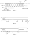
- FIG. 3 represents an exemplary embodiment of the memory unit 106 of each pixel 102 of the device 100 according to a first embodiment.
- the memory unit 106 of the pixel 102 also comprises a multiplexer 114 comprising two data inputs coupled to the sequencing unit 108. One of these two inputs is coupled to a first output of the sequencing unit 108 on which the display signal is sent. The other of these two inputs is coupled to a second output of the sequencing unit 108 on which the storage signal is sent.
- the multiplexer 114 also comprises a control input coupled to a third output of the sequencing unit 108 on which a selection signal is sent.
- the output of the multiplexer 114 is coupled to a control input of each of N first flip-flops 112, i.e. flip-flops 112.1 to 112.N.
- the control input of the last flip-flop 112.N+1 is not coupled to the output of the multiplexer 114.
- the control input of the last flip-flop 112.N+1 is coupled to the first output of the sequencing unit 108 on which the display signal is delivered.
- the display and storage signals may be such that during at least part of the display of a bit of the binary word of a first image, here the MSB of this binary word, the storage of the N-1 other bits of the binary word of the first image and of a bit of the binary word of a second image intended to be displayed after the first image, here the MSB of the binary word of the second image, is triggered.
- the binary words received by the pixels 102 are such that the N bits of each binary word sent successively, in series, to the input of the memory unit 106, are ordered such that the weight of the bits received is decreasing with the order of arrival at the input of the memory unit 106, and therefore that the MSB of the binary word is received first and that the LSB of the binary word is received last at the input of the memory unit 106.
- the timeline shown on the figure 4 corresponds to the selection, storage and display signals sent by the sequencing unit 108 to the memory unit 106 in this first configuration.
- a pulse of the display signal triggers the shift of the MSB of the binary word of the first image of the flip-flop 112.N in the flip-flop 112.N+1.
- the pixel 102 sends or not, for the duration corresponding to this MSB (corresponding to the time interval between the times t0 and t4 represented on the figure 4 ), a light signal.
- the selection signal changes value so that the storage signal is transmitted to the control inputs of the N flip-flops 112.1 to 112.N.
- the storage signal comprises 8 pulses triggering the storage, in the N flip-flops 112.N to 112.1, of the remaining 7 bits (from MSB-1 to LSB) of the binary word of the first image as well as the MSB of the binary word of the second image.
- the MSB-1 of the binary word of the first image is stored in the flip-flop 112.N
- the LSB of the binary word of the first image is stored in flip-flop 112.2
- the MSB of the binary word of the second image is stored in flip-flop 112.1.
- the selection signal changes value so that the display signal is again transmitted to the control inputs of the N flip-flops 112.1 to 112.N.
- Pulses of the display signal appearing at times t4 to t10 cause the bits stored in flip-flops 112.1 to 112.N to be shifted so that each of these bits is stored in flip-flop 112.N+1 for the duration corresponding to the weight of each of these bits (from MSB-1 to LSB). From time t10, the sequence of signals described above begins again using the binary words of the following image.
- the display and storage signals may be such that during at least part of the display of a bit of the binary word of a first image, here the MSB of this binary word, the storage of the N bits of the binary word of the second image intended to be displayed after the first image is triggered.
- the binary words received by the pixels 102 are such that the N bits of each binary word sent successively, in series, to the input of the memory unit 106, are ordered such that the weight of the bits received increases with the order of arrival at the input of the memory unit 106, and therefore that the LSB of the binary word is received first and that the MSB of the binary word is received last at the input of the memory unit 106.
- the timeline shown on the figure 5 corresponds to the selection, storage and display signals sent by the sequencing unit 108 to the memory unit 106 in this first configuration.
- the N bits of the binary word of the first image are stored in the flip-flops 112.1 to 112.N.
- Pulses of the display signal appearing at times t0 to t6 cause the bits stored in the flip-flops 112.1 to 112.N to be shifted so that each of these bits is stored in the flip-flop 112.N+1 for the duration corresponding to the weight of each of these bits (from the LSB to the MSB-1).
- a pulse of the display signal triggers the shift of the MSB of the binary word of the first image from the flip-flop 112.N to the flip-flop 112.N+1.
- the selection signal changes value so that the storage signal is transmitted to the control inputs of the N flip-flops 112.1 to 112.N.
- the storage signal comprises 8 pulses triggering the storage, in the N flip-flops 112.N to 112.1, of the 8 bits (from the LSB to the MSB) of the binary word of the second image.
- the LSB of the binary word of the second image is stored in the flip-flop 112.N and the MSB of the binary word of the second image is stored in the flip-flop 112.1.
- the selection signal changes value so that the display signal is again transmitted to the control inputs of the N flip-flops 112.1 to 112.N. From time t10, the sequence of signals described above begins again using the binary words of the following image, the N bits of which will be stored when displaying the MSB of the second image.
- the memory unit 106 of each pixel 102 may comprise a number of flip-flops 112 less than N+1 and greater than or equal to 3.
- the memory unit 106 of each pixel 102 may comprise 5 flip-flops 112.1 to 112.5.
- the 1st bit for example the MSB
- the following four bits 2nd , 3rd , 4th and 5th bits of the binary word
- the bits of each binary word are therefore stored during two successive storage phases.
- the embodiment example given above can be applied for a different number of flip-flops 112 and/or for binary words having a different number of bits. This example can be applied as much for binary words where the first bit received in the memory unit 106 corresponds to the most significant bit as for binary words where the first bit received in the memory unit 106 corresponds to the least significant bit, or any other order of arrival of the bits.
- the display unit 104 comprises a single light-emitting diode and the memory unit 106 comprises a single input configured to receive the binary words of the images to be displayed and three control inputs on which the display signal, the storage signal and the selection signal are received.
- FIG. 6 represents an exemplary embodiment of the memory unit 106 of each pixel 102 of the device 100 according to a second embodiment.
- the memory unit 106 comprises the N+1 flip-flops 112.
- the display and storage signals are combined to form a single display and storage signal.
- This combination is for example achieved by an OR gate 116 receiving on each of its two inputs one of the display and storage signals.
- the OR gate 116 can be formed within the sequencing unit 108 or outside the sequencing unit 108.
- the display and storage signal obtained at the output of the OR gate 116 is sent to a control input of each of the first N flip-flops 112.1 to 112.N.
- only the control input of the last of the N+1 flip-flops 112.N+1 does not receive the display and storage signal.
- the memory unit 106 also comprises a multiplexer 118 comprising two data inputs, one of which receives the display and storage signal and the other of which is coupled to an electrical reference potential, for example the ground called GND.
- the multiplexer 118 also comprises a control input coupled to the third output of the sequencing unit on which the selection signal is sent.
- the output of the multiplexer 118 is coupled to the control input of the last flip-flop 112.N+1.
- the display unit 104 here comprises a single light-emitting diode and the memory unit 106 comprises a single input configured to receive the binary words of the images to be displayed.
- the display and storage signal is sent to the control input of the N+1 flip-flops 112 and the pulses from the initial display signal which are received by the flip-flops 112.1 to 112.N+1 shift the bits stored in these flip-flops in the direction from the first flip-flop 112.1 to the last flip-flop 112.N+1 so that each of these bits are displayed for a duration corresponding to their respective weight.
- the selection signal changes value so that the control input of the last flip-flop 112.N+1 no longer receives the display and storage signal but receives the reference electrical potential applied to the other input of the multiplexer 118.
- the pulses from the initial storage signal and located in the display and storage signal are then applied to the first N flip-flops 112.1 to 112.N in order to trigger the storage, in these flip-flops, of the following bits to be displayed.
- the sequence described above then begins again using the binary words from the next image.
- FIG. 7 represents the selection signal and the display and storage signal when displaying an image, when the binary words received by the pixels 102 are such that the N bits of each binary word sent successively, in series, to the input of the memory unit 106, are ordered such that the weight of the bits received increases with the order of arrival at the input of the memory unit 106, and therefore that the LSB of the binary word is received first and the MSB of the binary word is received last at the input of the memory unit 106.
- this second embodiment is compatible with binary words such that the N bits of each binary word sent successively, in series, to the input of the memory unit 106, are ordered such that the weight of the bits received is decreasing with the order of arrival at the input of the memory unit 106, and therefore that the MSB of the binary word is received first and that the LSB of the binary word is received last at the input of the memory unit 106.
- the display and storage signal is obtained by performing a logical OR operation between the display signal and the storage signal within the sequencing unit 108.
- the memory unit 106 comprises only two control inputs on which the display and storage signal and the selection signal are received.
- the logic operation for obtaining the display and storage signal could be performed within the pixels 102, or could be obtained from the display signal and the storage signal using one or more elements other than an OR gate, in the sequencing unit 108 or outside the sequencing unit 108.
- each pixel 102 may comprise a number of flip-flops 112 less than N+1 and greater than or equal to 3, as previously described for the first embodiment.
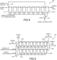
- FIG. 9 represents an exemplary embodiment of the memory unit 106 of each pixel 102 of the device 100 according to a third embodiment.
- the memory unit 106 of each pixel 102 comprises N first flip-flops 122.1 to 122.N coupled in series with each other.
- a data input of a first of the N first flip-flops 122.1 is coupled to an input of the pixel 102 intended to receive the binary words of the images to be displayed.
- the memory unit 106 also includes N second flip-flops 124.1 to 124.N coupled in series with each other. A data input of a first of the N second flip-flops 124.1 is coupled to the input of the pixel 102.
- the display unit 104 here comprises a single light-emitting diode and the memory unit 106 here comprises a single input configured to receive the binary words of the images to be displayed.
- the memory unit 106 further comprises a multiplexer 128 comprising two data inputs, one of which is coupled to the output of a last of the N first flip-flops 122.N and the other of which is coupled to the output of a last of the N second flip-flops 124.N.
- the multiplexer 128 also comprises a control input coupled to the third output of the sequencing unit on which the selection signal is delivered, and an output coupled to the input of the display unit 104.
- the signals sent by the sequencing unit 108 are such that when the first N flip-flops 122 receive the display signal on their control inputs, the output of the multiplexer 128 is coupled to the data input which is coupled to the output of the last of the first N flip-flops 122.N.
- the bits stored in the first N flip-flops 122 are displayed. successively by the display unit 104 on the control of the pulses of the display signal.
- the switching circuit 126 sends the storage signal to the control inputs of the second N flip-flops 124 which store the bits of the binary word applied to the input of the first of the second N flip-flops 124.1.
- the selection signal changes value, thus reversing the role of the first N flip-flops 122 and the second N flip-flops 124.
- the second N flip-flops 124 receive the display signal on their control inputs, and the output of the multiplexer 128 is coupled to the data input which is coupled to the output of the last of the second N flip-flops 124.N.
- the bits stored in the second N flip-flops 124 are displayed successively by the display unit 104 on the control of the pulses of the display signal.
- the switching circuit 126 sends the storage signal to the control inputs of the N first flip-flops 122 which store the bits of the binary word applied to the input of the first of the N first flip-flops 122.1.
- the selection signal After displaying the N bits stored in the second N flip-flops 124, the selection signal changes value again, reversing the role of the first N flip-flops 122 and the second N flip-flops 124.
- the first N flip-flops 122 and the second N flip-flops 124 therefore alternately fulfill the role of memory in which the bits of the binary word of a next image to be displayed are stored and the role of memory from which the bits of the binary word of an image to be displayed are sent to the display unit 104.
- this third embodiment is compatible with binary words such that the N bits of each binary word sent successively, in series, to the input of the memory unit 106, are ordered such that the weight of the bits received is decreasing with the order of arrival at the input of the memory unit 106, and therefore that the MSB of the binary word is received first and the LSB of the binary word is received last at the input of the memory unit 106, or such that the weight of the bits received is increasing with the order of arrival at the input of the memory unit 106, and therefore that the LSB of the binary word is received first and the MSB of the binary word is received last on the input of the memory unit 106.
- each pixel 102 may comprise less than 2.N flip-flops 122, 124, with at least two first flip-flops 122 and at least two second flip-flops 124, as previously described in connection with the first embodiment.
- FIG 10 represents an exemplary embodiment of the memory unit 106 of each pixel 102 of the device 100 according to a fourth embodiment.
- the memory unit 106 comprises N+1 memory elements 130.
- the memory unit 106 also comprises a first addressing circuit 133 comprising a data input coupled to an input of the pixel 102 intended to receive the binary words of the images to be displayed, N+1 outputs each coupled to an input of one of the N+1 memory elements 130, and at least one control input coupled to at least a first output of the sequencing unit 108 on which the storage signal is intended to be delivered.
- a first addressing circuit 133 comprising a data input coupled to an input of the pixel 102 intended to receive the binary words of the images to be displayed, N+1 outputs each coupled to an input of one of the N+1 memory elements 130, and at least one control input coupled to at least a first output of the sequencing unit 108 on which the storage signal is intended to be delivered.
- the first addressing circuit 133 comprises a first address generator 132 comprising an input coupled to the first output of the sequencing unit 108 on which the storage signal is intended to be delivered.
- the first addressing circuit 133 further comprises a demultiplexer 134 comprising a data input coupled to the input of the pixel 102 intended to receive the binary words of the images to be displayed, N+1 outputs each coupled to an input of one of the N+1 memory elements 130, and a control input coupled to an output of the first address generator 132.
- the demultiplexer 134 also comprises a second control input to which a validation signal is applied, authorizing or not the transfer of data from the input of the demultiplexer 134 to an output of the demultiplexer 134.
- the memory unit 106 also comprises a second addressing circuit 137 comprising N+1 data inputs each coupled to an output of one of the N+1 memory elements 130, an output coupled to an input of the display unit 104, and at least one control input coupled to at least a second output of the sequencing unit 108 on which the display signal is intended to be delivered.
- a second addressing circuit 137 comprising N+1 data inputs each coupled to an output of one of the N+1 memory elements 130, an output coupled to an input of the display unit 104, and at least one control input coupled to at least a second output of the sequencing unit 108 on which the display signal is intended to be delivered.
- the second addressing circuit 137 comprises a second address generator 136 comprising an input coupled to the second output of the sequencing unit 108 on which the display signal is intended to be delivered.
- the second addressing circuit 137 also includes a multiplexer 138 comprising N+1 data inputs each coupled to an output of one of the N+1 memory elements 130, an output coupled to the input of the display unit 104, and a control input coupled to an output of the second address generator 136.
- the display unit 104 comprises a light-emitting diode and the memory unit 106 comprises a single input configured to receive the binary words of the images to be displayed.
- the first address generator 132 delivers to the demultiplexer 134 a first address signal encoding on several bits the address of one of the N+1 memory elements 130 in which said one of the N bits of the binary word is stored.
- the second address generator 136 delivers to the multiplexer 138 a second address signal encoding on several bits the address of one of the N+1 memory elements 130 from which one of the N bits of the binary word is read.
- the memorization of the bits of a binary word of an image to be displayed is carried out during the display of a bit by the display unit, or even during the display of several bits by the display unit as is the case for the third embodiment previously described.
- the first and second address generators 132, 136 correspond for example to pseudo-random generators configured to deliver signals coded on several bits corresponding to the addresses of the memory elements 130.
- the sequencing unit 108 it is possible for the sequencing unit 108 to be configured such that the storage signal is formed of several first addressing signals each controlling a storage in one of the memory elements 130.
- the first addressing circuit 133 does not include the first address generator 132 since the write addressing is carried out directly by these first addressing signals.
- the sequencing unit 108 can be configured such that the display signal is formed of several second addressing signals each controlling a reading of a bit stored in one of the memory elements 130.
- the second addressing circuit 137 does not include the second address generator 136 since the reading addressing is carried out directly by the second addressing signals.
- This second configuration makes it possible to save the active surface occupied by the first and second address generators 132, 136, with the counterpart of increasing the number of interconnections linked to the pixels 102.
- the first addressing circuit 133 may comprise a first counter comprising an input coupled to the first output of the sequencing unit 108, and a first address decoder comprising a data input coupled to the input of the pixel 102 intended to receive the binary words, several outputs each coupled to the input of one of the memory elements 130, and a control input coupled to an output of the first counter.
- the second addressing circuit 137 comprises a second counter comprising an input coupled to the second output of the sequencing unit 108, a second address decoder comprising several data inputs each coupled to the output of one of the memory elements 130, an output coupled to the input of the display unit 104, and a control input coupled to an output of the second counter.
- the different configurations of the fourth embodiment can be combined with each other, that is to say that the first addressing circuit 133 can be produced according to one of the first, second and third configurations, and the second addressing circuit 137 can be produced according to another of these three configurations.
- This fourth embodiment has the advantage of allowing the choice of the order in which reading and writing are carried out in the memory elements 130.
- this fourth embodiment is compatible with binary words such that the N bits of each binary word sent successively, in series, to the input of the memory unit 106, are ordered such that the weight of the bits received is decreasing with the order of arrival at the input of the memory unit 106, and therefore the MSB of the binary word is received first and the LSB of the binary word is received last at the input of the memory unit 106, or such that the weight of the bits received is increasing with the order of arrival at the input of the memory unit 106, and therefore the LSB of the binary word is received first and the MSB of the binary word is received last at the input of the memory unit 106, or any other order.
- the memory unit 106 may comprise N memory elements 130.
- the phase of storing the bits of the binary words is preferably executed during the display of a bit corresponding to an MSB.
- the time available for storing the N bits in the memory unit 106 is equivalent to half the display time of an image.
- this storage phase it is however possible for this storage phase to be executed during the display of a bit other than an MSB. This is the case when several successive storage phases are implemented to store the bits of a single binary word.
- the order of storing and/or reading the bits does not necessarily correspond to the increasing order (from LSB to MSB) or decreasing order (from MSB to LSB) of the weight of the bits, the bits being able to be read and/or stored in any order.
- the phase of storing the bits of binary words can be executed for only part of the duration of display of a bit, for example for half the duration of the MSB.
- Such a variant can be implemented by using a memory unit 106 in which the output of the Nth flip-flop 112.N is looped back to the data input of the first flip-flop 112.1, as is the case on the figure 8 .
- the switch 120 is closed during this phase so that the value of the MSB is reloaded into the first flip-flop 112.1 after the other bits have been stored.
- the second half of the duration of the MSB is then displayed after the other bits have been displayed.
- Such a variant can also be implemented by adding an additional flip-flop for storing the value of the bit that is displayed over two non-consecutive halves of duration, thereby making it possible to have two flip-flops storing the value of that bit.
- each pixel 102 comprises a display unit 104 comprising a light-emitting diode.
- the display unit 104 of each pixel 102 may comprise several light-emitting diodes.
- each pixel 102 is intended to display an elementary point of an image which may correspond to a light signal emitted by a single light-emitting diode, or which may correspond to the sum of several light signals emitted by several light-emitting diodes, as is the case for a color display device.
- the memory unit 106 of each pixel 102 comprises a number of inputs configured to receive the binary words of the images to be displayed by the display unit 104 which is greater than or equal to 1 and which is less than or equal to M, with M corresponding to an integer greater than or equal to 1. It is for example possible to have as many light-emitting diodes as there are inputs configured to receive the binary words of the images to be displayed, for example 4.
- each pixel 102 is produced in the form of a module 101 produced and hybridized on a substrate 103 and comprising several second parts 109.1 - 109.4 forming the emissive parts (for example light-emitting diodes) of the module 101 (four in the example of the figure 13 , for example one emitting red light, another emitting blue light, and the other two emitting green light) and arranged on a first part 107 common to the second parts 109 of the module 101.
- the first part 107 comprises electronic elements produced using technology CMOS, forming in particular the memory unit 106 of the pixel 102 as well as the control element of each of the diodes of the pixel 102.
- the memory unit 106 formed in the first part 107 is configured to store at least part of the bits of the binary words intended to be displayed by the light-emitting diodes of the module.
- This configuration has the particular advantage of reducing the number of electrical connections dedicated to the control of the pixel 102 (corresponding to the signals other than the data signal, i.e. the binary words of the image to be displayed) to be made between the substrate 103 and the first part 107 of the module 101, because these connections are shared by the light-emitting diodes of the module 101.
- a part of the memory unit 106 of a pixel 102 is not formed in the first parts 107 of the module(s) 101 of this pixel 102, but is formed in an electronic circuit 111 distinct from the modules 101 and hybridized on the substrate 103, next to the module(s) 101 forming the light-emitting diode(s) of the pixel 102.
- figure 14 represents such a configuration in which four modules 101.1-101.4 each forming one of the four light-emitting diodes of a pixel 102 are hybridized on a substrate 103 by connection elements 105.
- the memory unit 106 in which the binary words of the pixel 102 are stored comprises elements or components distributed in the first parts 107 of the four modules 101.1-101.4 as well as in the circuit 111 hybridized on the substrate 103 by means of connectors 105.
- the first part 107 of each of the modules 101 comprising one of the light-emitting diodes ensures the storage of at least one of the bits of the binary word to be displayed, and comprises for example at least one flip-flop or any other element (for example a capacitor) ensuring this storage.
- the circuit 111 can also form at least one part of the sequencing unit 108.
- the first part 107 of each module 101 of a pixel 102 stores at least one bit of a binary word to be displayed.
- the number of control signals (signals other than the data signal(s) comprising the binary words to be displayed) received by each pixel 102 via the connection elements 105 is less than the number of memory elements N (flip-flops 112 or memory elements 130 for the examples described above) of the pixel 102.
- the number of connection elements 105 is less than N/2, or even between 5 and 10.
- each module 101 can be coupled to the substrate 103 via at least 5 connection elements (and equal to 5 when the module 101 comprises a single light-emitting diode): one dedicated to supplying the electrical supply potential, one dedicated to supplying a reference electrical potential, one dedicated to the selection signal, one dedicated to the display and storage, one dedicated to the data signal to be displayed.
- each memory unit 106 may be coupled to a plurality of light-emitting diodes of a display unit 104 to store binary words to be displayed by those light-emitting diodes.
- the number of flip-flops 112 described above for each pixel 102 may be multiplied by the number of light-emitting diodes to which each memory unit 106 is coupled.
- the number of memory elements 130 described above for each pixel 102 may be multiplied by the number of light-emitting diodes to which each memory unit 106 is coupled.
- FIG. 15 represents an exemplary embodiment of a memory unit 106 coupled to two light-emitting diodes 104.1 and 104.2 of the same pixel 102.
- the memory unit 106 is shared and associated with two light-emitting diodes.
- the memory unit 106 comprises two groups of memory elements 130.1 - 130.N+1 each associated with one of the light-emitting diodes 104.1, 104.2.
- the memory unit 106 also comprises the first address generator 132 comprising inputs coupled to the outputs of the sequencing unit 108 on which the storage signal and the display signal are intended to be delivered.
- the memory unit 106 further comprises the first addressing circuit 133, for example produced according to the first configuration, i.e. formed by the demultiplexer 134 comprising a data input coupled to an input of the pixel 102 intended to receive the binary words of the images, several sets of N+1 outputs (twice N+1 outputs in the example of the figure 15 ) each coupled to an input of one of the memory elements 130, and a control input coupled to an output of the first address generator 132.
- the first addressing circuit 133 for example produced according to the first configuration, i.e. formed by the demultiplexer 134 comprising a data input coupled to an input of the pixel 102 intended to receive the binary words of the images, several sets of N+1 outputs (twice N+1 outputs in the example of the figure 15 ) each coupled to an input of one of the memory elements 130, and a control input coupled to an output of the first address generator 132.
- the memory unit 106 also comprises the second addressing circuit 137, for example formed by the second address generator 136 comprising inputs coupled to the outputs of the sequencing unit 108 on which the storage signal and the display signal are intended to be delivered.
- the second addressing circuit 137 for example formed by the second address generator 136 comprising inputs coupled to the outputs of the sequencing unit 108 on which the storage signal and the display signal are intended to be delivered.
- the second addressing circuit 137 also comprises two multiplexers 138.1, 138.2 each comprising N+1 data inputs each coupled to an output of one of the memory elements 130, an output coupled to the input of the display unit 104 associated with it, and a control input coupled to an output of the second address generator 136.
- this memory unit 106 performs the storage of bits for two light-emitting diodes 104.
Landscapes
- Engineering & Computer Science (AREA)
- Physics & Mathematics (AREA)
- Computer Hardware Design (AREA)
- General Physics & Mathematics (AREA)
- Theoretical Computer Science (AREA)
- Control Of Indicators Other Than Cathode Ray Tubes (AREA)
Applications Claiming Priority (2)
| Application Number | Priority Date | Filing Date | Title |
|---|---|---|---|
| FR1852972A FR3079957B1 (fr) | 2018-04-05 | 2018-04-05 | Dispositif et procede d'affichage d'images avec une memorisation de donnees realisee dans les pixels |
| EP19167485.2A EP3550550A1 (de) | 2018-04-05 | 2019-04-05 | Bildanzeigevorrichtung und -verfahren mit einer datenspeicherung in den pixeln |
Related Parent Applications (1)
| Application Number | Title | Priority Date | Filing Date |
|---|---|---|---|
| EP19167485.2A Division EP3550550A1 (de) | 2018-04-05 | 2019-04-05 | Bildanzeigevorrichtung und -verfahren mit einer datenspeicherung in den pixeln |
Publications (1)
| Publication Number | Publication Date |
|---|---|
| EP4418247A1 true EP4418247A1 (de) | 2024-08-21 |
Family
ID=62167582
Family Applications (2)
| Application Number | Title | Priority Date | Filing Date |
|---|---|---|---|
| EP19167485.2A Ceased EP3550550A1 (de) | 2018-04-05 | 2019-04-05 | Bildanzeigevorrichtung und -verfahren mit einer datenspeicherung in den pixeln |
| EP24165631.3A Pending EP4418247A1 (de) | 2018-04-05 | 2019-04-05 | Bildanzeigevorrichtung und verfahren mit in pixeln hergestellter datenspeicherung |
Family Applications Before (1)
| Application Number | Title | Priority Date | Filing Date |
|---|---|---|---|
| EP19167485.2A Ceased EP3550550A1 (de) | 2018-04-05 | 2019-04-05 | Bildanzeigevorrichtung und -verfahren mit einer datenspeicherung in den pixeln |
Country Status (3)
| Country | Link |
|---|---|
| US (1) | US10902792B2 (de) |
| EP (2) | EP3550550A1 (de) |
| FR (1) | FR3079957B1 (de) |
Families Citing this family (4)
| Publication number | Priority date | Publication date | Assignee | Title |
|---|---|---|---|---|
| FR3123493B1 (fr) | 2021-05-26 | 2023-05-26 | Commissariat Energie Atomique | Dispositif d’affichage a adressage par groupes de pixels |
| FR3126262B1 (fr) | 2021-08-18 | 2024-08-30 | Commissariat Energie Atomique | Dispositif d’affichage a compression et decompression locales des donnees numeriques affichees |
| FR3129747B1 (fr) | 2021-11-29 | 2024-09-06 | Commissariat Energie Atomique | Dispositif d’affichage a dechiffrement local des donnees numeriques |
| CN116564218B (zh) * | 2022-01-29 | 2025-10-31 | 苏州佳世达电通有限公司 | 可改善鬼影现象的显示装置及相关驱动方法 |
Citations (5)
| Publication number | Priority date | Publication date | Assignee | Title |
|---|---|---|---|---|
| EP0391755A2 (de) * | 1989-03-03 | 1990-10-10 | Société dite: CENTAURE SA | Bildanzeigesystem |
| WO2002069259A2 (en) * | 2001-02-21 | 2002-09-06 | Three-Five Systems, Inc. | A system for controlling gray scale |
| US20030011314A1 (en) * | 2001-05-15 | 2003-01-16 | Takaji Numao | Display apparatus and display method |
| US20050083274A1 (en) * | 2003-07-30 | 2005-04-21 | Aaron Beddes | Sub-pulse width modulation for gamma correction and dimming control |
| FR3034902A1 (fr) | 2015-04-10 | 2016-10-14 | Commissariat Energie Atomique | Procede d’affichage d’images sur un ecran matriciel |
Family Cites Families (5)
| Publication number | Priority date | Publication date | Assignee | Title |
|---|---|---|---|---|
| JP2001308710A (ja) * | 2000-04-21 | 2001-11-02 | Sony Corp | 変調回路およびこれを用いた画像表示装置ならびに変調方法 |
| JP2001312246A (ja) * | 2000-05-01 | 2001-11-09 | Sony Corp | 変調回路およびこれを用いた画像表示装置 |
| JP2001350439A (ja) * | 2000-06-06 | 2001-12-21 | Sony Corp | 変調回路およびこれを用いた画像表示装置 |
| CA2873476A1 (en) * | 2014-12-08 | 2016-06-08 | Ignis Innovation Inc. | Smart-pixel display architecture |
| US10832609B2 (en) * | 2017-01-10 | 2020-11-10 | X Display Company Technology Limited | Digital-drive pulse-width-modulated output system |
-
2018
- 2018-04-05 FR FR1852972A patent/FR3079957B1/fr active Active
-
2019
- 2019-04-04 US US16/375,422 patent/US10902792B2/en active Active
- 2019-04-05 EP EP19167485.2A patent/EP3550550A1/de not_active Ceased
- 2019-04-05 EP EP24165631.3A patent/EP4418247A1/de active Pending
Patent Citations (5)
| Publication number | Priority date | Publication date | Assignee | Title |
|---|---|---|---|---|
| EP0391755A2 (de) * | 1989-03-03 | 1990-10-10 | Société dite: CENTAURE SA | Bildanzeigesystem |
| WO2002069259A2 (en) * | 2001-02-21 | 2002-09-06 | Three-Five Systems, Inc. | A system for controlling gray scale |
| US20030011314A1 (en) * | 2001-05-15 | 2003-01-16 | Takaji Numao | Display apparatus and display method |
| US20050083274A1 (en) * | 2003-07-30 | 2005-04-21 | Aaron Beddes | Sub-pulse width modulation for gamma correction and dimming control |
| FR3034902A1 (fr) | 2015-04-10 | 2016-10-14 | Commissariat Energie Atomique | Procede d’affichage d’images sur un ecran matriciel |
Also Published As
| Publication number | Publication date |
|---|---|
| EP3550550A1 (de) | 2019-10-09 |
| US20190311681A1 (en) | 2019-10-10 |
| US10902792B2 (en) | 2021-01-26 |
| FR3079957B1 (fr) | 2021-09-24 |
| FR3079957A1 (fr) | 2019-10-11 |
Similar Documents
| Publication | Publication Date | Title |
|---|---|---|
| EP3649672B1 (de) | Led anzeigevorrichtung | |
| EP3550550A1 (de) | Bildanzeigevorrichtung und -verfahren mit einer datenspeicherung in den pixeln | |
| FR2542119A1 (fr) | Procede pour commander un ecran d'affichage matriciel a cristaux liquides | |
| EP3965153B1 (de) | Led-emissionsbildanzeigevorrichtung | |
| EP3079142B1 (de) | Bildanzeigeverfahren auf matrix-bildschirm | |
| FR2762704A1 (fr) | Procede d'adressage pour ecran a plasma base sur une repetition de bits sur une ou plusieurs lignes | |
| EP4060650B1 (de) | Led-emissionsanzeigevorrichtung | |
| EP0597772A1 (de) | Multiplexbetriebener Matrixbildschirm und Steuerverfahren dafür | |
| WO2023110604A1 (fr) | Pixel d'affichage a diodes electroluminescentes pour ecran d'affichage | |
| FR2732495A1 (fr) | Procede de commande d'affichage | |
| FR2762703A1 (fr) | Procede et dispositif d'adressage a code tournant pour ecrans a plasma | |
| EP0907945B1 (de) | Verfahren zum aktivieren von bildschirmzellen und anzeigegerät zur durchführung dieses verfahrens | |
| EP2366246B1 (de) | Integriertes schaltungsarray und insbesondere gross bemessener bildsensor | |
| EP1354309A1 (de) | Digitaler video-bildschirm | |
| FR3137484A1 (fr) | Pixel d'affichage comprenant des diodes électroluminescentes et un écran d'affichage ayant de tels pixels d'affichage | |
| FR2803076A1 (fr) | Procede d'adressage de panneau d'affichage au plasma | |
| FR3137485A1 (fr) | Pixel d'affichage comprenant des sources électroluminescentes | |
| EP3549124B1 (de) | Adressierungsmodus und konstruktionsprinzip von matrixbildschirmen zur anzeige von farbbildern mit quasi-statistischem verhalten | |
| EP2104092B1 (de) | Anzeigevorrichtung, die in einem Sondermodus zur Anzeige mit geringem Energieverbrauch betrieben werden kann | |
| FR3126262A1 (fr) | Dispositif d’affichage a compression et decompression locales des donnees numeriques affichees | |
| FR3104795A1 (fr) | Dispositif comprenant un écran d'affichage à mode de fonctionnement à basse consommation | |
| FR3150639A1 (fr) | Ecran d'affichage comportant des pixels d'affichage comprenant des sources luminescentes | |
| EP1864275A1 (de) | Bildanzeigeeinrichtung und verfahren zu ihrer steuerung | |
| FR3156970A1 (fr) | Dispositif de pilotage d’une interface vidéo pour une matrice de circuits d’affichage | |
| FR3150040A1 (fr) | Pixel d'affichage comprenant des diodes électroluminescentes pour un écran d'affichage |
Legal Events
| Date | Code | Title | Description |
|---|---|---|---|
| PUAI | Public reference made under article 153(3) epc to a published international application that has entered the european phase |
Free format text: ORIGINAL CODE: 0009012 |
|
| STAA | Information on the status of an ep patent application or granted ep patent |
Free format text: STATUS: REQUEST FOR EXAMINATION WAS MADE |
|
| 17P | Request for examination filed |
Effective date: 20240322 |
|
| AC | Divisional application: reference to earlier application |
Ref document number: 3550550 Country of ref document: EP Kind code of ref document: P |
|
| AK | Designated contracting states |
Kind code of ref document: A1 Designated state(s): AL AT BE BG CH CY CZ DE DK EE ES FI FR GB GR HR HU IE IS IT LI LT LU LV MC MK MT NL NO PL PT RO RS SE SI SK SM TR |
|
| RAP3 | Party data changed (applicant data changed or rights of an application transferred) |
Owner name: COMMISSARIAT A L'ENERGIE ATOMIQUE ET AUX ENERGIESALTERNATIVES |
|
| STAA | Information on the status of an ep patent application or granted ep patent |
Free format text: STATUS: EXAMINATION IS IN PROGRESS |