EP4420859A1 - Dispositif de lithographie laser et procédé de génération d'une structure tridimensionnelle - Google Patents
Dispositif de lithographie laser et procédé de génération d'une structure tridimensionnelle Download PDFInfo
- Publication number
- EP4420859A1 EP4420859A1 EP24152852.0A EP24152852A EP4420859A1 EP 4420859 A1 EP4420859 A1 EP 4420859A1 EP 24152852 A EP24152852 A EP 24152852A EP 4420859 A1 EP4420859 A1 EP 4420859A1
- Authority
- EP
- European Patent Office
- Prior art keywords
- protective device
- lithography
- laser
- lens
- writing beam
- Prior art date
- Legal status (The legal status is an assumption and is not a legal conclusion. Google has not performed a legal analysis and makes no representation as to the accuracy of the status listed.)
- Pending
Links
Images


Classifications
-
- G—PHYSICS
- G03—PHOTOGRAPHY; CINEMATOGRAPHY; ANALOGOUS TECHNIQUES USING WAVES OTHER THAN OPTICAL WAVES; ELECTROGRAPHY; HOLOGRAPHY
- G03F—PHOTOMECHANICAL PRODUCTION OF TEXTURED OR PATTERNED SURFACES, e.g. FOR PRINTING, FOR PROCESSING OF SEMICONDUCTOR DEVICES; MATERIALS THEREFOR; ORIGINALS THEREFOR; APPARATUS SPECIALLY ADAPTED THEREFOR
- G03F7/00—Photomechanical, e.g. photolithographic, production of textured or patterned surfaces, e.g. printing surfaces; Materials therefor, e.g. comprising photoresists; Apparatus specially adapted therefor
- G03F7/70—Microphotolithographic exposure; Apparatus therefor
- G03F7/708—Construction of apparatus, e.g. environment aspects, hygiene aspects or materials
- G03F7/7095—Materials, e.g. materials for housing, stage or other support having particular properties, e.g. weight, strength, conductivity, thermal expansion coefficient
- G03F7/70958—Optical materials or coatings, e.g. with particular transmittance, reflectance or anti-reflection properties
-
- B—PERFORMING OPERATIONS; TRANSPORTING
- B29—WORKING OF PLASTICS; WORKING OF SUBSTANCES IN A PLASTIC STATE IN GENERAL
- B29C—SHAPING OR JOINING OF PLASTICS; SHAPING OF MATERIAL IN A PLASTIC STATE, NOT OTHERWISE PROVIDED FOR; AFTER-TREATMENT OF THE SHAPED PRODUCTS, e.g. REPAIRING
- B29C64/00—Additive manufacturing, i.e. manufacturing of three-dimensional [3D] objects by additive deposition, additive agglomeration or additive layering, e.g. by 3D printing, stereolithography or selective laser sintering
- B29C64/20—Apparatus for additive manufacturing; Details thereof or accessories therefor
- B29C64/264—Arrangements for irradiation
- B29C64/268—Arrangements for irradiation using laser beams; using electron beams [EB]
-
- B—PERFORMING OPERATIONS; TRANSPORTING
- B23—MACHINE TOOLS; METAL-WORKING NOT OTHERWISE PROVIDED FOR
- B23K—SOLDERING OR UNSOLDERING; WELDING; CLADDING OR PLATING BY SOLDERING OR WELDING; CUTTING BY APPLYING HEAT LOCALLY, e.g. FLAME CUTTING; WORKING BY LASER BEAM
- B23K26/00—Working by laser beam, e.g. welding, cutting or boring
-
- B—PERFORMING OPERATIONS; TRANSPORTING
- B23—MACHINE TOOLS; METAL-WORKING NOT OTHERWISE PROVIDED FOR
- B23K—SOLDERING OR UNSOLDERING; WELDING; CLADDING OR PLATING BY SOLDERING OR WELDING; CUTTING BY APPLYING HEAT LOCALLY, e.g. FLAME CUTTING; WORKING BY LASER BEAM
- B23K26/00—Working by laser beam, e.g. welding, cutting or boring
- B23K26/0006—Working by laser beam, e.g. welding, cutting or boring taking account of the properties of the material involved
-
- B—PERFORMING OPERATIONS; TRANSPORTING
- B23—MACHINE TOOLS; METAL-WORKING NOT OTHERWISE PROVIDED FOR
- B23K—SOLDERING OR UNSOLDERING; WELDING; CLADDING OR PLATING BY SOLDERING OR WELDING; CUTTING BY APPLYING HEAT LOCALLY, e.g. FLAME CUTTING; WORKING BY LASER BEAM
- B23K26/00—Working by laser beam, e.g. welding, cutting or boring
- B23K26/02—Positioning or observing the workpiece, e.g. with respect to the point of impact; Aligning, aiming or focusing the laser beam
- B23K26/04—Automatically aligning, aiming or focusing the laser beam, e.g. using the back-scattered light
- B23K26/046—Automatically focusing the laser beam
-
- B—PERFORMING OPERATIONS; TRANSPORTING
- B23—MACHINE TOOLS; METAL-WORKING NOT OTHERWISE PROVIDED FOR
- B23K—SOLDERING OR UNSOLDERING; WELDING; CLADDING OR PLATING BY SOLDERING OR WELDING; CUTTING BY APPLYING HEAT LOCALLY, e.g. FLAME CUTTING; WORKING BY LASER BEAM
- B23K26/00—Working by laser beam, e.g. welding, cutting or boring
- B23K26/02—Positioning or observing the workpiece, e.g. with respect to the point of impact; Aligning, aiming or focusing the laser beam
- B23K26/06—Shaping the laser beam, e.g. by masks or multi-focusing
- B23K26/064—Shaping the laser beam, e.g. by masks or multi-focusing by means of optical elements, e.g. lenses, mirrors or prisms
- B23K26/0648—Shaping the laser beam, e.g. by masks or multi-focusing by means of optical elements, e.g. lenses, mirrors or prisms comprising lenses
-
- B—PERFORMING OPERATIONS; TRANSPORTING
- B23—MACHINE TOOLS; METAL-WORKING NOT OTHERWISE PROVIDED FOR
- B23K—SOLDERING OR UNSOLDERING; WELDING; CLADDING OR PLATING BY SOLDERING OR WELDING; CUTTING BY APPLYING HEAT LOCALLY, e.g. FLAME CUTTING; WORKING BY LASER BEAM
- B23K26/00—Working by laser beam, e.g. welding, cutting or boring
- B23K26/08—Devices involving relative movement between laser beam and workpiece
- B23K26/082—Scanning systems, i.e. devices involving movement of the laser beam relative to the laser head
-
- B—PERFORMING OPERATIONS; TRANSPORTING
- B23—MACHINE TOOLS; METAL-WORKING NOT OTHERWISE PROVIDED FOR
- B23K—SOLDERING OR UNSOLDERING; WELDING; CLADDING OR PLATING BY SOLDERING OR WELDING; CUTTING BY APPLYING HEAT LOCALLY, e.g. FLAME CUTTING; WORKING BY LASER BEAM
- B23K26/00—Working by laser beam, e.g. welding, cutting or boring
- B23K26/70—Auxiliary operations or equipment
- B23K26/702—Auxiliary equipment
-
- B—PERFORMING OPERATIONS; TRANSPORTING
- B29—WORKING OF PLASTICS; WORKING OF SUBSTANCES IN A PLASTIC STATE IN GENERAL
- B29C—SHAPING OR JOINING OF PLASTICS; SHAPING OF MATERIAL IN A PLASTIC STATE, NOT OTHERWISE PROVIDED FOR; AFTER-TREATMENT OF THE SHAPED PRODUCTS, e.g. REPAIRING
- B29C64/00—Additive manufacturing, i.e. manufacturing of three-dimensional [3D] objects by additive deposition, additive agglomeration or additive layering, e.g. by 3D printing, stereolithography or selective laser sintering
- B29C64/10—Processes of additive manufacturing
- B29C64/106—Processes of additive manufacturing using only liquids or viscous materials, e.g. depositing a continuous bead of viscous material
-
- B—PERFORMING OPERATIONS; TRANSPORTING
- B29—WORKING OF PLASTICS; WORKING OF SUBSTANCES IN A PLASTIC STATE IN GENERAL
- B29C—SHAPING OR JOINING OF PLASTICS; SHAPING OF MATERIAL IN A PLASTIC STATE, NOT OTHERWISE PROVIDED FOR; AFTER-TREATMENT OF THE SHAPED PRODUCTS, e.g. REPAIRING
- B29C64/00—Additive manufacturing, i.e. manufacturing of three-dimensional [3D] objects by additive deposition, additive agglomeration or additive layering, e.g. by 3D printing, stereolithography or selective laser sintering
- B29C64/20—Apparatus for additive manufacturing; Details thereof or accessories therefor
- B29C64/205—Means for applying layers
- B29C64/209—Heads; Nozzles
-
- B—PERFORMING OPERATIONS; TRANSPORTING
- B33—ADDITIVE MANUFACTURING TECHNOLOGY
- B33Y—ADDITIVE MANUFACTURING, i.e. MANUFACTURING OF THREE-DIMENSIONAL [3D] OBJECTS BY ADDITIVE DEPOSITION, ADDITIVE AGGLOMERATION OR ADDITIVE LAYERING, e.g. BY 3D PRINTING, STEREOLITHOGRAPHY OR SELECTIVE LASER SINTERING
- B33Y10/00—Processes of additive manufacturing
-
- B—PERFORMING OPERATIONS; TRANSPORTING
- B33—ADDITIVE MANUFACTURING TECHNOLOGY
- B33Y—ADDITIVE MANUFACTURING, i.e. MANUFACTURING OF THREE-DIMENSIONAL [3D] OBJECTS BY ADDITIVE DEPOSITION, ADDITIVE AGGLOMERATION OR ADDITIVE LAYERING, e.g. BY 3D PRINTING, STEREOLITHOGRAPHY OR SELECTIVE LASER SINTERING
- B33Y30/00—Apparatus for additive manufacturing; Details thereof or accessories therefor
-
- B—PERFORMING OPERATIONS; TRANSPORTING
- B33—ADDITIVE MANUFACTURING TECHNOLOGY
- B33Y—ADDITIVE MANUFACTURING, i.e. MANUFACTURING OF THREE-DIMENSIONAL [3D] OBJECTS BY ADDITIVE DEPOSITION, ADDITIVE AGGLOMERATION OR ADDITIVE LAYERING, e.g. BY 3D PRINTING, STEREOLITHOGRAPHY OR SELECTIVE LASER SINTERING
- B33Y40/00—Auxiliary operations or equipment, e.g. for material handling
-
- G—PHYSICS
- G02—OPTICS
- G02B—OPTICAL ELEMENTS, SYSTEMS OR APPARATUS
- G02B27/00—Optical systems or apparatus not provided for by any of the groups G02B1/00 - G02B26/00, G02B30/00
- G02B27/0006—Optical systems or apparatus not provided for by any of the groups G02B1/00 - G02B26/00, G02B30/00 with means to keep optical surfaces clean, e.g. by preventing or removing dirt, stains, contamination, condensation
-
- G—PHYSICS
- G03—PHOTOGRAPHY; CINEMATOGRAPHY; ANALOGOUS TECHNIQUES USING WAVES OTHER THAN OPTICAL WAVES; ELECTROGRAPHY; HOLOGRAPHY
- G03F—PHOTOMECHANICAL PRODUCTION OF TEXTURED OR PATTERNED SURFACES, e.g. FOR PRINTING, FOR PROCESSING OF SEMICONDUCTOR DEVICES; MATERIALS THEREFOR; ORIGINALS THEREFOR; APPARATUS SPECIALLY ADAPTED THEREFOR
- G03F7/00—Photomechanical, e.g. photolithographic, production of textured or patterned surfaces, e.g. printing surfaces; Materials therefor, e.g. comprising photoresists; Apparatus specially adapted therefor
- G03F7/0037—Production of three-dimensional images
-
- G—PHYSICS
- G03—PHOTOGRAPHY; CINEMATOGRAPHY; ANALOGOUS TECHNIQUES USING WAVES OTHER THAN OPTICAL WAVES; ELECTROGRAPHY; HOLOGRAPHY
- G03F—PHOTOMECHANICAL PRODUCTION OF TEXTURED OR PATTERNED SURFACES, e.g. FOR PRINTING, FOR PROCESSING OF SEMICONDUCTOR DEVICES; MATERIALS THEREFOR; ORIGINALS THEREFOR; APPARATUS SPECIALLY ADAPTED THEREFOR
- G03F7/00—Photomechanical, e.g. photolithographic, production of textured or patterned surfaces, e.g. printing surfaces; Materials therefor, e.g. comprising photoresists; Apparatus specially adapted therefor
- G03F7/20—Exposure; Apparatus therefor
- G03F7/2051—Exposure without an original mask, e.g. using a programmed deflection of a point source, by scanning, by drawing with a light beam, using an addressed light or corpuscular source
- G03F7/2053—Exposure without an original mask, e.g. using a programmed deflection of a point source, by scanning, by drawing with a light beam, using an addressed light or corpuscular source using a laser
-
- G—PHYSICS
- G03—PHOTOGRAPHY; CINEMATOGRAPHY; ANALOGOUS TECHNIQUES USING WAVES OTHER THAN OPTICAL WAVES; ELECTROGRAPHY; HOLOGRAPHY
- G03F—PHOTOMECHANICAL PRODUCTION OF TEXTURED OR PATTERNED SURFACES, e.g. FOR PRINTING, FOR PROCESSING OF SEMICONDUCTOR DEVICES; MATERIALS THEREFOR; ORIGINALS THEREFOR; APPARATUS SPECIALLY ADAPTED THEREFOR
- G03F7/00—Photomechanical, e.g. photolithographic, production of textured or patterned surfaces, e.g. printing surfaces; Materials therefor, e.g. comprising photoresists; Apparatus specially adapted therefor
- G03F7/70—Microphotolithographic exposure; Apparatus therefor
- G03F7/70416—2.5D lithography
-
- G—PHYSICS
- G03—PHOTOGRAPHY; CINEMATOGRAPHY; ANALOGOUS TECHNIQUES USING WAVES OTHER THAN OPTICAL WAVES; ELECTROGRAPHY; HOLOGRAPHY
- G03F—PHOTOMECHANICAL PRODUCTION OF TEXTURED OR PATTERNED SURFACES, e.g. FOR PRINTING, FOR PROCESSING OF SEMICONDUCTOR DEVICES; MATERIALS THEREFOR; ORIGINALS THEREFOR; APPARATUS SPECIALLY ADAPTED THEREFOR
- G03F7/00—Photomechanical, e.g. photolithographic, production of textured or patterned surfaces, e.g. printing surfaces; Materials therefor, e.g. comprising photoresists; Apparatus specially adapted therefor
- G03F7/70—Microphotolithographic exposure; Apparatus therefor
- G03F7/708—Construction of apparatus, e.g. environment aspects, hygiene aspects or materials
- G03F7/70983—Optical system protection, e.g. pellicles or removable covers for protection of mask
-
- G—PHYSICS
- G02—OPTICS
- G02B—OPTICAL ELEMENTS, SYSTEMS OR APPARATUS
- G02B21/00—Microscopes
- G02B21/33—Immersion oils, or microscope systems or objectives for use with immersion fluids
Definitions
- the invention relates to a laser lithography device and a method for producing a three-dimensional structure by means of a laser lithography device.
- laser lithography is also known as stereo lithography or direct laser writing.
- structures are written using a laser writing beam into a usually initially liquid, photosensitive substance, which in this context is referred to as Lithography material is referred to as a lithographic material.
- the laser writing beam triggers a local solidification effect in the lithography material.
- the solidification occurs, for example, due to a local polymerization of the lithography material induced by photon absorption.
- photoresist In the field of stereolithography, it is also referred to as resin.
- the technology of laser lithography or direct laser writing is advantageously used in the production of micro or nano structures when high precision is desired and at the same time freedom of design and flexibility in shaping are to be maintained.
- different structures can be written without the structure being predetermined by a mask or something similar.
- the desired overall structure is created by sequentially writing a series of substructures (for example layer by layer or slice by slice), which then complement each other to form the desired structure.
- the writing beam hits the surface of a volume of lithographic material and leads to local solidification on the surface.
- These methods are generally based on linear processes such as single-photon absorption and the resulting local change in the lithographic material.
- an additional layer of lithographic material is applied in an application step after a layer has been written. This can be achieved, for example, by gradually lowering a substrate with the structure to be written onto it into a bath of lithographic material and structuring the surface using the writing beam. With such techniques it can happen that the end element of the focusing optics comes into contact with lithographic material.
- Another approach uses the physical principle of two-photon polymerization or generally multi-photon polymerization to achieve solidification of lithographic material even within a volume of lithographic material, i.e. also below the surface.
- the writing beam and the lithographic material are coordinated in such a way that a solidification effect occurs with the involvement of non-linear effects.
- the writing beam is selected in a spectral range that normally cannot trigger a solidification effect in the lithographic material.
- lithographic material and Writing beams must be coordinated in such a way that induced solidification can only occur through radiation that has a wavelength that corresponds to a fraction (in particular an integer fraction) of the wavelength of the writing beam actually used.
- the term multi-photon polymerization refers to induced polymerization through the simultaneous absorption of two or more than two photons.
- the term "multi-photon absorption" for the present description also includes the process of "two-photon absorption” and "two-stage absorption".
- the conditions required for multi-photon polymerization are generally only achieved in a zone of increased intensity. This zone of increased intensity is provided in a focus area of the laser writing beam.
- the focus area is a beam waist of the laser writing beam, which is generated by suitable optics (e.g. beam guidance optics, beam shaping optics and/or a lens).
- suitable optics e.g. beam guidance optics, beam shaping optics and/or a lens.
- the focus area can then be moved through a volume of lithographic material according to geometry description data and trigger a local solidification process.
- the production of three-dimensional structures using two-photon polymerization is often carried out at a working distance of 100 ⁇ m to 20 mm.
- the working distance is a distance between the focus area and an optical end element of a lens for generating the focus area. At such short working distances, contact between the lens and the lithography material can often not be prevented.
- the lens is often immersed in the lithography material.
- a manufacturing process in which the lens is at least partially immersed in the lithography material can also be referred to as dip-in multi-photon polymerization. Therefore, the lithography material often comes into contact with the lens and in particular the optical end element during the production of three-dimensional structures.
- DE 101 11 422 A1 shows 3D laser lithography using multi-photon polymerization within a bath of lithography material in a container.
- the device described here has an exit optic for focusing the laser beam on a focus area within the container.
- EN 10 2011 012 484 A1 discloses 3D laser lithography utilizing multi-photon polymerization within a liquid lithography material, wherein an objective lens of the laser optics is immersed in the lithography material.
- EN 10 2018 221 670 A1 describes a device for optically processing an object.
- the device comprises an objective for exposing the object by means of a light beam, wherein a membrane is arranged between the objective and the object and is spaced apart from the objective.
- the membrane is movable in the direction of an optical axis of the light beam, wherein positioning elements enable the movement of the membrane.
- the invention is based on the object of providing a laser lithography device and a method for producing a three-dimensional structure using the laser lithography device.
- the laser lithography device should preferably be compatible with a large number of different lithography materials.
- the lens has an optical closure element.
- the laser lithography device further comprises a scanning device for shifting the focus area of the laser writing beam relative to the lithography material and a protective device for preventing contact between the optical closure element and the lithography material.
- the protective device is arranged on the optical closure element.
- the protective device By arranging the protective device on the optical end element, direct contact between the optical end element and the lithography material can be prevented, in particular when the lens is immersed in the lithography material. This can, for example, prevent problems when lithography materials are used that contain dyes or components that damage the optical end element when they come into contact with it. Furthermore, the cleaning effort of the lens after the three-dimensional structure has been created can advantageously be significantly reduced; in particular, cleaning the lens can be omitted entirely when the protective device is replaced.
- the propagation path of the laser writing beam within the lithography material can advantageously be reduced by choosing a suitable thickness of the protective device, which is why, when using highly absorbent lithography materials, it is ensured that sufficient power of the laser writing beam reaches the focus area to ensure a to induce polymerization of the lithography material. Therefore, due to the protection device, the laser lithography device is compatible with a variety of different lithography materials.
- arranging the protective device on the optical termination element prevents contaminants from the optical termination element from being introduced into the lithography material. This prevents contamination of the lithography material and enables the creation of a sterile three-dimensional structure.
- the protective device can advantageously act as a buffer to reduce damage in the event of a collision of the lens with samples within the lithography material or an already created three-dimensional structure.
- the laser writing beam and the lithography material can be coordinated in such a way that the lithography material can be solidified locally within the focus area by means of multi-photon polymerization to produce the three-dimensional structure.
- the laser writing beam can be a continuous wave laser writing beam or a pulsed laser writing beam.
- a pulse of the pulsed laser writing beam can have a pulse duration of 50 femtoseconds to 500 nanoseconds.
- the lens may have a numerical apparatus in the range from 0.01 to 1.4 inclusive.
- the optical closure element can have an optical element through which the laser writing beam exits the lens.
- the optical closure element can comprise or form the optical element which delimits the lens, in particular with respect to the surroundings of the lens.
- the optical closure element can comprise or form a closure lens, in particular a converging lens, or a closure window, in particular a glass pane.
- the optical closure element can also comprise further means, e.g. an adhesive.
- the optical closure element can be fastened in a lens housing of the lens, for example by means of the adhesive.
- the shifting of the focus area of the laser writing beam relative to the lithography material can be achieved by deflecting the laser writing beam and/or by shifting the lithography material.
- the scanning device can be designed to shift the lithography material or a suitable carrier device (e.g. container, substrate, or similar) for the lithography material.
- the scanning device can comprise actuators, in particular servomotors or linear motors, which shift the lithography material.
- the scanning device can be designed to shift the focus area.
- the scanning device can a beam guidance and steering arrangement, for example in the form of scanner mirrors and/or acousto-optical deflectors. The beam guidance and steering arrangement can be arranged between the laser source and the objective or the optical end element.
- the beam guiding and steering arrangement may include a beam shaping module for adjusting focus sizes and/or for dynamically mapping complex intensity patterns.
- the beam shaping module may be arranged between the laser source and the objective.
- the protective device can be designed as a single piece.
- the protective device can be designed separately from the lens.
- the protective device can be designed to prevent contact between the optical closure element and the lithography material when the lens is immersed in the lithography material.
- the protective device can be designed to be partially and/or completely immersed in the lithography material.
- the protective device can have a refractive index that differs from a refractive index of the lithography material. However, the refractive index can preferably also be the same.
- the protective device can have a refractive index that differs from a refractive index of the optical terminating element. The However, the refractive index can preferably also be the same.
- the protective device can have a refractive index that has a value that lies between a value of the refractive index of the optical terminating element and a value of the refractive index of the lithography material.
- the protective device can have a thickness of 2 pm to 4 mm, in particular 2 pm to 500 pm, in particular 300 pm or 60 pm.
- the protective device can be arranged detachably on the optical closure element. This advantageously allows the protective device to be replaced if, for example, deposits of the lithography material are present on the protective device.
- the protective device can be arranged on the optical closure element in such a way that a hollow space, for example an air chamber, between the optical closure element and the protective device is avoided.
- the protective device can be arranged directly on the optical closure element, in particular in a sealing manner there.
- the protective device can have a touching contact with the optical closure element.
- the protective device can cover the optical closure element.
- the protective device comprises a film or a foil.
- the film or foil can be arranged relatively easily on the optical end element and is inexpensive.
- the film or foil can be arranged on the optical end element.
- the film or foil can be a homogeneous sheet made of very thin plastic.
- the film or foil can have a thickness of 2 pm to 4 mm, in particular 2 pm to 500 pm, in particular 300 pm or 60 pm.
- the protective device can, in particular only, be a film or foil. In particular, the protective device can preferably only consist of a film or foil.
- the protective device is designed to be attached to the optical end element.
- the protective device can be designed to be attached to the optical end element by means of loose molecular bonds, in particular Van der Waals bonds.
- the protective device can be an adhesive film that is designed to be attached to the optical end element by means of adhesion.
- the protective device can comprise a holder for attaching the protective device to the lens.
- the holder can be an O-ring.
- the protective device has an adhesive layer for fastening the protective device to the optical closure element.
- the protective device can be attached particularly easily and reliably by means of the Adhesive layer can be attached to the optical end element.
- the adhesive layer can be arranged on the optical end element.
- the adhesive layer can have a thickness of 2 pm to 100 pm, in particular 2 pm to 50 pm, in particular 20 pm.
- the protective device can, in particular, only be a sticker, in particular an adhesive tape.
- the sticker can comprise the adhesive layer and the film or foil.
- the protective device can preferably only consist of a sticker.
- conventional adhesive tapes or adhesive foils can be used in a simple manner.
- a transmission level of the protective device for the laser writing beam is at least 80%, in particular 85%, 90%, 92%, 95% or 98%.
- a high transmission level advantageously ensures that sufficient power of the laser writing beam reaches the focus area to induce polymerization of the lithography material.
- the lens has a lens housing.
- the optical closure element is accommodated, in particular held, by the lens housing.
- the lens housing often has at least one element that is unsuitable for contact with the lithography material.
- the protective device then preferably also covers said element in order to prevent contact between the element and the Lithography material. This advantageously allows the lens to penetrate particularly deeply into the lithography material.
- the element may be considered unsuitable for contact with the lithographic material if, for example, in the event of contact, the element is damaged or a high level of cleaning is required to remove the lithographic material from the element.
- High level of cleaning may be understood to mean that cleaning by wiping with a clean cloth is not sufficient to remove the lithographic material from the element.
- the element can comprise a recess in the lens housing, for example in the form of a groove or a thread.
- the lens housing can comprise two housing parts, wherein the lens housing has a recess in the form of a groove at a connection point of both housing parts.
- the element can comprise an operating element for correcting imaging errors.
- the operating element can comprise a correction ring.
- Image errors can be chromatic aberration and/or spherical aberration.
- the protective device has a refractive index that can be corrected by the lens.
- the lens can be corrected for the refractive index of the protective device and, with a suitable choice of the thickness of the protective device, a propagation path of the laser writing beam within the lithography material can be reduced in such a way that the lithography material can have a refractive index that cannot be corrected by the lens.
- lithography materials whose refractive index cannot be corrected by the lens can also be used to produce the three-dimensional structure.
- the protective device has a first layer with a first refractive index and a second layer with a second refractive index.
- the first refractive index differs from the second refractive index.
- the first layer can be the adhesive layer.
- the refractive index of the protective device can advantageously be adjusted by means of the first layer and the second layer. In particular, the refractive index of the protective device can be adjusted in such a way that it can be corrected by the lens.
- the first layer can be on the optical end element.
- the first layer can be arranged between the optical end element and the second layer.
- the refractive index of the protective device can be a combination of the first refractive index and the second refractive index.
- the laser lithography device comprises a further protective device for preventing contact between the optical closure element and the lithography material.
- the further protective device is arranged on the previously described first protective device.
- a propagation path of the laser writing beam within the lithography material can be reduced by means of the protective device and the further protective device.
- the additional protective device can cover the protective device.
- the additional protective device can be the same as the protective device.
- the additional protective device can differ from the first protective device in thickness or refractive index.
- the thickness of the (first) protective device can be 60 pm and the thickness of the additional protective device can be 100 pm.
- a method according to the invention for producing a three-dimensional structure in a lithography material is carried out by means of a previously described laser lithography device.
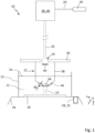
- Fig.1 shows a schematic representation of a laser lithography device 10 for producing a three-dimensional structure in a lithography material 12.
- the lithography material 12 is a liquid, photosensitive substance which is held in a container 14 and has a lithography material surface 16.
- the laser lithography device 10 has a laser source 18 for emitting a laser writing beam 20 and a lens 22 for focusing the laser writing beam 20 in a focus area 24.
- the three-dimensional structure is produced by local solidification, in particular local polymerization, of the lithography material 12 as a result of multi-photon absorption within the focus area 24.
- the three-dimensional structure is to be produced on a substrate 26, which is arranged within the container 14 and is surrounded by the lithography material 12.
- designs without a substrate and/or without a container can also be advantageous.
- the laser lithography device 10 has a scanning device 28 for shifting the focus area 24 of the laser writing beam 20 relative to the lithography material 12.
- the scanning device 28 has a beam guidance and steering arrangement 30 and actuators 32 in the form of servo motors (here, for example, three).
- the beam guidance and steering arrangement 30 is arranged within an optical path of the laser writing beam 20.
- the beam guidance and steering arrangement 30 deflects the laser writing beam 20.
- the beam guidance and steering arrangement 30 comprises a beam shaping module that shapes the laser writing beam 20, for example based on geometry description data of the three-dimensional structure to be created.
- the actuators 32 are arranged on a container holder 34 of the laser lithography device 10 for the purpose of displacing the container holder 34 in three mutually orthogonal spatial directions x, y, z.
- Each of the three servomotors of the actuators 32 causes a displacement in one of the spatial directions x, y, z.
- the container holder 34 is displaced based on geometry description data of the three-dimensional structure to be created.
- the lens 22 is mounted on a head plate 36 of the laser lithography device 10.
- the head plate 36 can be displaced by means of further actuators of the scanning device 28.
- the lens 22 has a lens housing 38 mounted to the head plate 36 such that an entrance aperture 40 of the lens 22 corresponds to a corresponding opening 42 of the head plate 36.
- the laser writing beam 20 propagates through the opening 42 and through the entrance aperture 40 along the optical path.
- the lens 22 has an optical end element 44 in the form of a closing lens.
- the optical end element 44 is held by the lens housing 38.
- the closing element 44 forms the transition from the lens 22.
- the laser lithography device 10 has a protective device 46 for preventing contact between the optical closure element 44 and the lithography material 12.
- the protective device 46 is arranged directly on the optical closure element 44 so that the protective device 46 has a touching contact with the optical closure element 44.
- the protective device 46 completely covers the optical closure element 44.
- the protective device 46 partially covers the lens housing 38.
- the laser writing beam 20 exits the lens 22 through the optical closure element 44 and propagates through the protective device 46 to subsequently form the focus area 24.
- a transmission factor of the protective device 44 for the laser writing beam 20 is preferably at least 90%.
- the lens 22 is immersed in the lithography material 12 to create the three-dimensional structure.
- the optical closure element 44 is located below the lithography material surface 16.
- the protective device 46 prevents in an immersed State of the lens 22 a contact between the optical closure element 44 and the lithography material 12. Therefore, the protection device 46 enables the lens 22 to be immersed in the lithography material 12 without the optical closure element 44 being impaired by the lithography material 12 (eg soiled or damaged).
- the protective device 46 is a sticker in the form of an adhesive tape.
- the protective device 46 preferably consists only of the adhesive tape, which comprises an adhesive layer and a film.
- the adhesive layer is a first layer with a first refractive index.
- the film is a second layer with a second refractive index.
- the first refractive index can differ from the second refractive index, but this is not mandatory.
- the effective refractive index of the protective device 46 is a combination of the first refractive index and the second refractive index.
- the film is attached, in particular glued, to the optical closure element 44 by means of the adhesive layer.
- the protective device 46 has a thickness 48 of 60 ⁇ m.
- Fig. 2 shows a sketched representation of the lens 22, wherein the lens 22 is immersed in the lithography material 12.
- the lithography material 12 is highly absorbent for the laser writing beam 20.
- the Laser writing beam 20 propagates within the lithography material 12 along a propagation path 50 that extends from the protective device 46 to the focus area 24. During propagation along the propagation path 50, the laser writing beam 20 is absorbed by the lithography material 12. Due to the protective device 46 with the thickness 48 of 60 pm, the propagation path 50 within the lithography material 12 has been reduced by 60 pm. Due to the reduced propagation path 50, more power of the laser writing beam 20 reaches the focus area 24.
- Fig.3 shows a sketched representation of the lens 22 of Fig.2 with a further protective device 52.
- the further protective device 52 is arranged on the protective device 46.
- the further protective device 52 covers the protective device 46.
- the further protective device 52 is designed in the example in the same way as the protective device 46, which is why reference is made to the description of the protective device 46 with regard to the features of the further protective device 52.
- Fig.4 shows a sketched representation of the lens 22 of Fig.3 with an additional (third) protective device 54.
- the additional protective device 54 is arranged on the further (second) protective device 52.
- the additional protective device 54 covers the further protective device 52.
- the additional protective device 54 is designed, for example, in the same way as the (first) protective device 46, which is why reference is made to the description of the protective device 46 with regard to the features of the additional protective device 54.
- the propagation path 50 of the laser writing beam 20 within the lithography material 12 is reduced in such a way that sufficient power of the laser writing beam 20 reaches the focus area 24 to induce polymerization of the lithography material 12.
- lithography materials that strongly absorb the laser writing beam 20 can be used to create the three-dimensional structure.
- the refractive index of the respective protective devices 46, 52, 54 differs, for example, from a refractive index of the lithographic material 12.
- a design is conceivable in which the refractive index of the Lithography material 12 cannot be corrected by the lens 22, which is why imaging errors in the form of chromatic aberration and/or spherical aberration occur when the laser writing beam 20 propagates within the lithography material 12.
- the refractive index of the respective protective devices 46, 52, 54 is corrected by the lens 22.
- the imaging errors are additionally reduced by arranging several protective devices 46, 52, 54.
- Fig.5 shows a further sketched representation of the lens 22.
- Contaminants 56 in the form of bacteria and viruses adhere to the optical end element 44.
- the protective device 46 is sterile and is arranged on the optical end element 44 in such a way that the contaminants 56 are not introduced into the lithography material 12, even if the lens 22 is immersed in the lithography material 12. This prevents contamination of the lithography material 12.
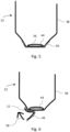
- Fig.6 shows a sketched representation of the lens 22 of Fig. 2 during the removal of the protective device 46.
- the lens 22 was used to create a three-dimensional structure and was immersed in the lithographic material 12.
- lithographic material 12 was deposited on the protective device 46.
- the protective device 46 in the form of the adhesive tape is simply peeled off the lens 22 in a peeling direction 58.
- the adhesive layer enables a residue-free removal of the protective device 46 from the optical end element 44.
- Figs. 7 and 8 are variants of the lens of the Fig. 1 to 6 and in Fig.8 is also a variant of the protective device of the Fig. 1 to 7 shown, whereby identical reference numerals are used for identical and functionally equivalent elements and in this respect reference is made to the above statements on the embodiment of the Fig. 1 to 6 or to the example of Fig. 1 to 7 can be referred to, so that essentially only the existing differences are discussed.
- Fig.7 shows a sketched representation of a variant 22 of the lens from Fig. 2 .
- the optical end element 44 is compared to the variant of the Fig. 1 to 6 held deeper within the lens housing 38.
- the lens housing 38 has a projection 60.
- the protective device 46 is moldable such that the protective device 46 is arranged on the optical closure element 44 without a cavity, for example an air chamber, between the optical closure element 44 and the protective device 46.
- the protective device 46 is moldable such that the protective device 46 rests on the projection 60 without forming a cavity.
- Fig.8 shows a sketched representation of another variant 22 of the lens from Fig. 2 and a variant 46 of the protective device of Fig. 1 to 7 .
- the protective device 46 consists only of a film in the form of an adhesive film.
- the adhesive film is a homogeneous surface structure made of very thin plastic with a thickness of 14 ⁇ m.
- the protective device 46 of the Fig.8 does not have an adhesive layer.
- the adhesive film is attached to the optical closure element 44 by means of adhesion.
- the lens housing 38 has, for example, an element 62 that is unsuitable for contact with the lithography material.
- the element 62 is an operating element in the form of a circumferential correction ring.
- imaging errors for example chromatic aberration and/or spherical aberration, can be corrected.
- the lithography material 12 gets on the element 62, the lithography material 12 can get inside the lens housing 38 and damage or contaminate the lens 22. Cleaning or repairing the lens 22 would be expensive.
- the protective device 46 completely covers the element 62. This allows the lens 22 to penetrate particularly deeply into the lithography material 12. In particular, the lens 22 can penetrate so deeply into the lithography material 12 that the element 62 is located below the lithography material surface 16.
- the protective device 46 may be an adhesive tape that completely covers the element 62.
Landscapes
- Physics & Mathematics (AREA)
- Engineering & Computer Science (AREA)
- Optics & Photonics (AREA)
- Chemical & Material Sciences (AREA)
- Mechanical Engineering (AREA)
- Materials Engineering (AREA)
- Plasma & Fusion (AREA)
- General Physics & Mathematics (AREA)
- Manufacturing & Machinery (AREA)
- Health & Medical Sciences (AREA)
- Public Health (AREA)
- Epidemiology (AREA)
- Environmental & Geological Engineering (AREA)
- Toxicology (AREA)
Applications Claiming Priority (1)
| Application Number | Priority Date | Filing Date | Title |
|---|---|---|---|
| DE102023104751.5A DE102023104751A1 (de) | 2023-02-27 | 2023-02-27 | Laserlithografie-Vorrichtung und Verfahren zum Erzeugen einer dreidimensionalen Struktur |
Publications (1)
| Publication Number | Publication Date |
|---|---|
| EP4420859A1 true EP4420859A1 (fr) | 2024-08-28 |
Family
ID=89662151
Family Applications (1)
| Application Number | Title | Priority Date | Filing Date |
|---|---|---|---|
| EP24152852.0A Pending EP4420859A1 (fr) | 2023-02-27 | 2024-01-19 | Dispositif de lithographie laser et procédé de génération d'une structure tridimensionnelle |
Country Status (4)
| Country | Link |
|---|---|
| US (1) | US20240288786A1 (fr) |
| EP (1) | EP4420859A1 (fr) |
| CN (1) | CN118543955A (fr) |
| DE (1) | DE102023104751A1 (fr) |
Citations (7)
| Publication number | Priority date | Publication date | Assignee | Title |
|---|---|---|---|---|
| DE10111422A1 (de) | 2001-03-09 | 2002-09-26 | Hannover Laser Zentrum | Verfahren und Vorrichtung zur Herstellung eines Formkörpers aus einem durch Bestrahlung zu verfestigenden flüssigen Material |
| DE102006016533A1 (de) * | 2006-04-07 | 2007-11-15 | Carl Zeiss Smt Ag | Haltevorrichtung für optisches Element |
| DE102011012484A1 (de) | 2011-02-25 | 2012-08-30 | Nanoscribe Gmbh | Verfahren und Vorrichtung zum ortsaufgelösten Einbringen eines Intensitätsmusters aus elektromagnetischer Strahlung in eine photosensitive Substanz sowie Verwendung hiervon |
| US20160299426A1 (en) * | 2013-12-06 | 2016-10-13 | 3M Innovative Properties Company | Semi-submersible microscope objective with protective element and use of the same in multiphoton imaging method |
| DE102018128418B3 (de) * | 2018-11-13 | 2019-11-14 | Nanoscribe Gmbh | Verwendung eines Dispenser-Aufsatzes und Dispenser-Aufsatz für eine Vorrichtung zum Schreiben von 3D-Strukturen mittels Laserlithografie |
| DE102018221670A1 (de) | 2018-12-13 | 2020-06-18 | Karlsruher Institut für Technologie | Vorrichtung und Verfahren zur optischen Charakterisierung oder Bearbeitung eines Objekts |
| US20220350127A1 (en) * | 2019-12-05 | 2022-11-03 | 3M Innovative Properties Company | Multiphoton Imaging Methods in a Scattering and/or Absorbing Medium, and Articles |
Family Cites Families (4)
| Publication number | Priority date | Publication date | Assignee | Title |
|---|---|---|---|---|
| US7460206B2 (en) * | 2003-12-19 | 2008-12-02 | Carl Zeiss Smt Ag | Projection objective for immersion lithography |
| JP4669302B2 (ja) * | 2005-02-24 | 2011-04-13 | 富士通株式会社 | レンズカバー |
| GB2431670A (en) * | 2005-10-25 | 2007-05-02 | Zeiss Carl Smt Ag | Protective coating with windows for protection of optical element that is soluble in immersion liquid. |
| US9158207B2 (en) * | 2011-08-09 | 2015-10-13 | Carl Zeiss Smt Gmbh | Optical component comprising radiation protective layer |
-
2023
- 2023-02-27 DE DE102023104751.5A patent/DE102023104751A1/de active Pending
-
2024
- 2024-01-19 EP EP24152852.0A patent/EP4420859A1/fr active Pending
- 2024-02-03 US US18/431,935 patent/US20240288786A1/en active Pending
- 2024-02-23 CN CN202410202202.8A patent/CN118543955A/zh active Pending
Patent Citations (7)
| Publication number | Priority date | Publication date | Assignee | Title |
|---|---|---|---|---|
| DE10111422A1 (de) | 2001-03-09 | 2002-09-26 | Hannover Laser Zentrum | Verfahren und Vorrichtung zur Herstellung eines Formkörpers aus einem durch Bestrahlung zu verfestigenden flüssigen Material |
| DE102006016533A1 (de) * | 2006-04-07 | 2007-11-15 | Carl Zeiss Smt Ag | Haltevorrichtung für optisches Element |
| DE102011012484A1 (de) | 2011-02-25 | 2012-08-30 | Nanoscribe Gmbh | Verfahren und Vorrichtung zum ortsaufgelösten Einbringen eines Intensitätsmusters aus elektromagnetischer Strahlung in eine photosensitive Substanz sowie Verwendung hiervon |
| US20160299426A1 (en) * | 2013-12-06 | 2016-10-13 | 3M Innovative Properties Company | Semi-submersible microscope objective with protective element and use of the same in multiphoton imaging method |
| DE102018128418B3 (de) * | 2018-11-13 | 2019-11-14 | Nanoscribe Gmbh | Verwendung eines Dispenser-Aufsatzes und Dispenser-Aufsatz für eine Vorrichtung zum Schreiben von 3D-Strukturen mittels Laserlithografie |
| DE102018221670A1 (de) | 2018-12-13 | 2020-06-18 | Karlsruher Institut für Technologie | Vorrichtung und Verfahren zur optischen Charakterisierung oder Bearbeitung eines Objekts |
| US20220350127A1 (en) * | 2019-12-05 | 2022-11-03 | 3M Innovative Properties Company | Multiphoton Imaging Methods in a Scattering and/or Absorbing Medium, and Articles |
Also Published As
| Publication number | Publication date |
|---|---|
| DE102023104751A1 (de) | 2024-08-29 |
| US20240288786A1 (en) | 2024-08-29 |
| CN118543955A (zh) | 2024-08-27 |
Similar Documents
| Publication | Publication Date | Title |
|---|---|---|
| DE102011012484B4 (de) | Verfahren und Vorrichtung zum ortsaufgelösten Einbringen eines Intensitätsmusters aus elektromagnetischer Strahlung in eine photosensitive Substanz sowie Verwendung hiervon | |
| EP2184127B1 (fr) | Procédé de marquage au laser, utilisation d'un dispositif de marquage au laser et élément optique | |
| DE19520187C1 (de) | Optik zum Herstellen einer scharfen Beleuchtungslinie aus einem Laserstrahl | |
| DE102015012980B4 (de) | Verfahren zur Herstellung von Mikrostrukturen auf optischen Fasern | |
| DE102016214606B3 (de) | Verfahren und Vorrichtung zur lithographischen Erzeugung einer Zielstruktur an einer nicht-planaren Ausgangsstruktur | |
| DE102019200750A1 (de) | Herstellungsverfahren für Komponenten einer Projektionsbelichtungsanlage für die Halbleiterlithographie und Projektionsbelichtungsanlage | |
| EP0307874A2 (fr) | Méthode pour former une marque sur des lentilles de lunettes | |
| DE102008031937A1 (de) | Mehrstrahl-Laservorrichtung | |
| EP3653363B1 (fr) | Utilisation d'un adaptateur de distribution pour un dispositif d'écriture de structures tridimensionnelles par lithographie laser | |
| DE102014224717A1 (de) | Optisches Element, optische Anordnung und Herstellungsverfahren | |
| EP3894928B1 (fr) | Dispositif et procédé pour le traitement optique d'un objet | |
| EP4420859A1 (fr) | Dispositif de lithographie laser et procédé de génération d'une structure tridimensionnelle | |
| DE112022005635T5 (de) | Laser lift-off-verfahren, verfahren zum herstellen eines empfängersubstrats, einrichtung zum laser lift-off und fotomaske | |
| EP4275869B1 (fr) | Procédé et dispositif de génération d'une structure tridimensionnelle dans un fluide lithographique | |
| DE102021109579B4 (de) | Verfahren und vorrichtung zum ausbilden von modifikationen mit einem laserstrahl in einem material mit einer gekrümmten oberfläche | |
| DE112023002534T5 (de) | Projektor und verfahren zur herstellung optischer elemente für einen projektor | |
| DE102020130651B3 (de) | Vorrichtung zum Erzeugen einer definierten Laserbeleuchtung auf einer Arbeitsebene | |
| WO2024047256A1 (fr) | Substrat ayant des propriétés antibuée | |
| DE202014011053U1 (de) | Lithografieeinrichtung zum Herstellen einer Struktur | |
| DE10243737B3 (de) | Vorrichtung zur Bearbeitung eines Substrats mit Hilfe von Laserstrahlung | |
| DE102018203400A1 (de) | Flüssigkeitsentfernungsvorrichtung und flüssigkeitsentfernungsverfahren | |
| DE102023123551B4 (de) | Verfahren zum Erzeugen einer dreidimensionalen Struktur und Laserlithografie-Vorrichtung | |
| DE102007020704B4 (de) | Einrichtung für die Bearbeitung eines Werkstückes mit einem Laserstrahl | |
| DE102023123552A1 (de) | Laserlithografie-Vorrichtung zum Erzeugen einer dreidimensionalen Struktur und Verfahren zum Betreiben einer Laserlithografie-Vorrichtung | |
| DE102022127259B4 (de) | Verfahren sowie Vorrichtung zur Abbildung eines Strahls auf ein Objekt und Verfahren zum Einbringen einer Öffnung in ein Werkstück mittels dieses Verfahrens |
Legal Events
| Date | Code | Title | Description |
|---|---|---|---|
| PUAI | Public reference made under article 153(3) epc to a published international application that has entered the european phase |
Free format text: ORIGINAL CODE: 0009012 |
|
| STAA | Information on the status of an ep patent application or granted ep patent |
Free format text: STATUS: THE APPLICATION HAS BEEN PUBLISHED |
|
| AK | Designated contracting states |
Kind code of ref document: A1 Designated state(s): AL AT BE BG CH CY CZ DE DK EE ES FI FR GB GR HR HU IE IS IT LI LT LU LV MC ME MK MT NL NO PL PT RO RS SE SI SK SM TR |
|
| STAA | Information on the status of an ep patent application or granted ep patent |
Free format text: STATUS: REQUEST FOR EXAMINATION WAS MADE |
|
| 17P | Request for examination filed |
Effective date: 20241004 |
|
| RBV | Designated contracting states (corrected) |
Designated state(s): AL AT BE BG CH CY CZ DE DK EE ES FI FR GB GR HR HU IE IS IT LI LT LU LV MC ME MK MT NL NO PL PT RO RS SE SI SK SM TR |