EP4442425A1 - Verfahren zur herstellung eines tieretiketts sowie tieretikett - Google Patents
Verfahren zur herstellung eines tieretiketts sowie tieretikett Download PDFInfo
- Publication number
- EP4442425A1 EP4442425A1 EP24168540.3A EP24168540A EP4442425A1 EP 4442425 A1 EP4442425 A1 EP 4442425A1 EP 24168540 A EP24168540 A EP 24168540A EP 4442425 A1 EP4442425 A1 EP 4442425A1
- Authority
- EP
- European Patent Office
- Prior art keywords
- polymer material
- animal
- tag
- circuit board
- printed circuit
- Prior art date
- Legal status (The legal status is an assumption and is not a legal conclusion. Google has not performed a legal analysis and makes no representation as to the accuracy of the status listed.)
- Pending
Links
Images

Classifications
-
- G—PHYSICS
- G06—COMPUTING OR CALCULATING; COUNTING
- G06K—GRAPHICAL DATA READING; PRESENTATION OF DATA; RECORD CARRIERS; HANDLING RECORD CARRIERS
- G06K19/00—Record carriers for use with machines and with at least a part designed to carry digital markings
- G06K19/06—Record carriers for use with machines and with at least a part designed to carry digital markings characterised by the kind of the digital marking, e.g. shape, nature, code
- G06K19/067—Record carriers with conductive marks, printed circuits or semiconductor circuit elements, e.g. credit or identity cards also with resonating or responding marks without active components
- G06K19/07—Record carriers with conductive marks, printed circuits or semiconductor circuit elements, e.g. credit or identity cards also with resonating or responding marks without active components with integrated circuit chips
- G06K19/077—Constructional details, e.g. mounting of circuits in the carrier
- G06K19/0772—Physical layout of the record carrier
- G06K19/07724—Physical layout of the record carrier the record carrier being at least partially made by a molding process
-
- A—HUMAN NECESSITIES
- A01—AGRICULTURE; FORESTRY; ANIMAL HUSBANDRY; HUNTING; TRAPPING; FISHING
- A01K—ANIMAL HUSBANDRY; AVICULTURE; APICULTURE; PISCICULTURE; FISHING; REARING OR BREEDING ANIMALS, NOT OTHERWISE PROVIDED FOR; NEW BREEDS OF ANIMALS
- A01K11/00—Marking of animals
- A01K11/001—Ear-tags
- A01K11/004—Ear-tags with electronic identification means, e.g. transponders
-
- A—HUMAN NECESSITIES
- A01—AGRICULTURE; FORESTRY; ANIMAL HUSBANDRY; HUNTING; TRAPPING; FISHING
- A01K—ANIMAL HUSBANDRY; AVICULTURE; APICULTURE; PISCICULTURE; FISHING; REARING OR BREEDING ANIMALS, NOT OTHERWISE PROVIDED FOR; NEW BREEDS OF ANIMALS
- A01K11/00—Marking of animals
- A01K11/006—Automatic identification systems for animals, e.g. electronic devices, transponders for animals
-
- A—HUMAN NECESSITIES
- A01—AGRICULTURE; FORESTRY; ANIMAL HUSBANDRY; HUNTING; TRAPPING; FISHING
- A01K—ANIMAL HUSBANDRY; AVICULTURE; APICULTURE; PISCICULTURE; FISHING; REARING OR BREEDING ANIMALS, NOT OTHERWISE PROVIDED FOR; NEW BREEDS OF ANIMALS
- A01K29/00—Other apparatus for animal husbandry
- A01K29/005—Monitoring or measuring activity
-
- B—PERFORMING OPERATIONS; TRANSPORTING
- B29—WORKING OF PLASTICS; WORKING OF SUBSTANCES IN A PLASTIC STATE IN GENERAL
- B29C—SHAPING OR JOINING OF PLASTICS; SHAPING OF MATERIAL IN A PLASTIC STATE, NOT OTHERWISE PROVIDED FOR; AFTER-TREATMENT OF THE SHAPED PRODUCTS, e.g. REPAIRING
- B29C45/00—Injection moulding, i.e. forcing the required volume of moulding material through a nozzle into a closed mould; Apparatus therefor
- B29C45/14—Injection moulding, i.e. forcing the required volume of moulding material through a nozzle into a closed mould; Apparatus therefor incorporating preformed parts or layers, e.g. injection moulding around inserts or for coating articles
- B29C45/14467—Joining articles or parts of a single article
-
- B—PERFORMING OPERATIONS; TRANSPORTING
- B29—WORKING OF PLASTICS; WORKING OF SUBSTANCES IN A PLASTIC STATE IN GENERAL
- B29C—SHAPING OR JOINING OF PLASTICS; SHAPING OF MATERIAL IN A PLASTIC STATE, NOT OTHERWISE PROVIDED FOR; AFTER-TREATMENT OF THE SHAPED PRODUCTS, e.g. REPAIRING
- B29C45/00—Injection moulding, i.e. forcing the required volume of moulding material through a nozzle into a closed mould; Apparatus therefor
- B29C45/14—Injection moulding, i.e. forcing the required volume of moulding material through a nozzle into a closed mould; Apparatus therefor incorporating preformed parts or layers, e.g. injection moulding around inserts or for coating articles
- B29C45/14836—Preventing damage of inserts during injection, e.g. collapse of hollow inserts, breakage
-
- G—PHYSICS
- G06—COMPUTING OR CALCULATING; COUNTING
- G06K—GRAPHICAL DATA READING; PRESENTATION OF DATA; RECORD CARRIERS; HANDLING RECORD CARRIERS
- G06K19/00—Record carriers for use with machines and with at least a part designed to carry digital markings
- G06K19/06—Record carriers for use with machines and with at least a part designed to carry digital markings characterised by the kind of the digital marking, e.g. shape, nature, code
- G06K19/067—Record carriers with conductive marks, printed circuits or semiconductor circuit elements, e.g. credit or identity cards also with resonating or responding marks without active components
- G06K19/07—Record carriers with conductive marks, printed circuits or semiconductor circuit elements, e.g. credit or identity cards also with resonating or responding marks without active components with integrated circuit chips
- G06K19/077—Constructional details, e.g. mounting of circuits in the carrier
- G06K19/07749—Constructional details, e.g. mounting of circuits in the carrier the record carrier being capable of non-contact communication, e.g. constructional details of the antenna of a non-contact smart card
- G06K19/07773—Antenna details
-
- H—ELECTRICITY
- H05—ELECTRIC TECHNIQUES NOT OTHERWISE PROVIDED FOR
- H05K—PRINTED CIRCUITS; CASINGS OR CONSTRUCTIONAL DETAILS OF ELECTRIC APPARATUS; MANUFACTURE OF ASSEMBLAGES OF ELECTRICAL COMPONENTS
- H05K3/00—Apparatus or processes for manufacturing printed circuits
- H05K3/22—Secondary treatment of printed circuits
- H05K3/28—Applying non-metallic protective coatings
-
- B—PERFORMING OPERATIONS; TRANSPORTING
- B29—WORKING OF PLASTICS; WORKING OF SUBSTANCES IN A PLASTIC STATE IN GENERAL
- B29C—SHAPING OR JOINING OF PLASTICS; SHAPING OF MATERIAL IN A PLASTIC STATE, NOT OTHERWISE PROVIDED FOR; AFTER-TREATMENT OF THE SHAPED PRODUCTS, e.g. REPAIRING
- B29C45/00—Injection moulding, i.e. forcing the required volume of moulding material through a nozzle into a closed mould; Apparatus therefor
- B29C45/14—Injection moulding, i.e. forcing the required volume of moulding material through a nozzle into a closed mould; Apparatus therefor incorporating preformed parts or layers, e.g. injection moulding around inserts or for coating articles
- B29C45/14836—Preventing damage of inserts during injection, e.g. collapse of hollow inserts, breakage
- B29C2045/14844—Layers protecting the insert from injected material
-
- B—PERFORMING OPERATIONS; TRANSPORTING
- B29—WORKING OF PLASTICS; WORKING OF SUBSTANCES IN A PLASTIC STATE IN GENERAL
- B29C—SHAPING OR JOINING OF PLASTICS; SHAPING OF MATERIAL IN A PLASTIC STATE, NOT OTHERWISE PROVIDED FOR; AFTER-TREATMENT OF THE SHAPED PRODUCTS, e.g. REPAIRING
- B29C45/00—Injection moulding, i.e. forcing the required volume of moulding material through a nozzle into a closed mould; Apparatus therefor
- B29C45/14—Injection moulding, i.e. forcing the required volume of moulding material through a nozzle into a closed mould; Apparatus therefor incorporating preformed parts or layers, e.g. injection moulding around inserts or for coating articles
- B29C2045/14852—Injection moulding, i.e. forcing the required volume of moulding material through a nozzle into a closed mould; Apparatus therefor incorporating preformed parts or layers, e.g. injection moulding around inserts or for coating articles incorporating articles with a data carrier, e.g. chips
-
- B—PERFORMING OPERATIONS; TRANSPORTING
- B29—WORKING OF PLASTICS; WORKING OF SUBSTANCES IN A PLASTIC STATE IN GENERAL
- B29C—SHAPING OR JOINING OF PLASTICS; SHAPING OF MATERIAL IN A PLASTIC STATE, NOT OTHERWISE PROVIDED FOR; AFTER-TREATMENT OF THE SHAPED PRODUCTS, e.g. REPAIRING
- B29C45/00—Injection moulding, i.e. forcing the required volume of moulding material through a nozzle into a closed mould; Apparatus therefor
- B29C45/14—Injection moulding, i.e. forcing the required volume of moulding material through a nozzle into a closed mould; Apparatus therefor incorporating preformed parts or layers, e.g. injection moulding around inserts or for coating articles
- B29C2045/1486—Details, accessories and auxiliary operations
- B29C2045/14868—Pretreatment of the insert, e.g. etching, cleaning
-
- B—PERFORMING OPERATIONS; TRANSPORTING
- B29—WORKING OF PLASTICS; WORKING OF SUBSTANCES IN A PLASTIC STATE IN GENERAL
- B29C—SHAPING OR JOINING OF PLASTICS; SHAPING OF MATERIAL IN A PLASTIC STATE, NOT OTHERWISE PROVIDED FOR; AFTER-TREATMENT OF THE SHAPED PRODUCTS, e.g. REPAIRING
- B29C45/00—Injection moulding, i.e. forcing the required volume of moulding material through a nozzle into a closed mould; Apparatus therefor
- B29C45/14—Injection moulding, i.e. forcing the required volume of moulding material through a nozzle into a closed mould; Apparatus therefor incorporating preformed parts or layers, e.g. injection moulding around inserts or for coating articles
- B29C45/14639—Injection moulding, i.e. forcing the required volume of moulding material through a nozzle into a closed mould; Apparatus therefor incorporating preformed parts or layers, e.g. injection moulding around inserts or for coating articles for obtaining an insulating effect, e.g. for electrical components
-
- B—PERFORMING OPERATIONS; TRANSPORTING
- B29—WORKING OF PLASTICS; WORKING OF SUBSTANCES IN A PLASTIC STATE IN GENERAL
- B29C—SHAPING OR JOINING OF PLASTICS; SHAPING OF MATERIAL IN A PLASTIC STATE, NOT OTHERWISE PROVIDED FOR; AFTER-TREATMENT OF THE SHAPED PRODUCTS, e.g. REPAIRING
- B29C45/00—Injection moulding, i.e. forcing the required volume of moulding material through a nozzle into a closed mould; Apparatus therefor
- B29C45/16—Making multilayered or multicoloured articles
- B29C45/1615—The materials being injected at different moulding stations
-
- B—PERFORMING OPERATIONS; TRANSPORTING
- B29—WORKING OF PLASTICS; WORKING OF SUBSTANCES IN A PLASTIC STATE IN GENERAL
- B29C—SHAPING OR JOINING OF PLASTICS; SHAPING OF MATERIAL IN A PLASTIC STATE, NOT OTHERWISE PROVIDED FOR; AFTER-TREATMENT OF THE SHAPED PRODUCTS, e.g. REPAIRING
- B29C45/00—Injection moulding, i.e. forcing the required volume of moulding material through a nozzle into a closed mould; Apparatus therefor
- B29C45/16—Making multilayered or multicoloured articles
- B29C45/1671—Making multilayered or multicoloured articles with an insert
-
- B—PERFORMING OPERATIONS; TRANSPORTING
- B29—WORKING OF PLASTICS; WORKING OF SUBSTANCES IN A PLASTIC STATE IN GENERAL
- B29K—INDEXING SCHEME ASSOCIATED WITH SUBCLASSES B29B, B29C OR B29D, RELATING TO MOULDING MATERIALS OR TO MATERIALS FOR MOULDS, REINFORCEMENTS, FILLERS OR PREFORMED PARTS, e.g. INSERTS
- B29K2023/00—Use of polyalkenes or derivatives thereof as moulding material
-
- B—PERFORMING OPERATIONS; TRANSPORTING
- B29—WORKING OF PLASTICS; WORKING OF SUBSTANCES IN A PLASTIC STATE IN GENERAL
- B29K—INDEXING SCHEME ASSOCIATED WITH SUBCLASSES B29B, B29C OR B29D, RELATING TO MOULDING MATERIALS OR TO MATERIALS FOR MOULDS, REINFORCEMENTS, FILLERS OR PREFORMED PARTS, e.g. INSERTS
- B29K2077/00—Use of PA, i.e. polyamides, e.g. polyesteramides or derivatives thereof, as moulding material
-
- B—PERFORMING OPERATIONS; TRANSPORTING
- B29—WORKING OF PLASTICS; WORKING OF SUBSTANCES IN A PLASTIC STATE IN GENERAL
- B29L—INDEXING SCHEME ASSOCIATED WITH SUBCLASS B29C, RELATING TO PARTICULAR ARTICLES
- B29L2031/00—Other particular articles
- B29L2031/34—Electrical apparatus, e.g. sparking plugs or parts thereof
- B29L2031/3425—Printed circuits
Definitions
- the present invention is directed at a method of manufacturing an animal tag for use in an animal monitoring system, wherein the animal tag comprises a printed circuit board (PCB) for supporting an electronic circuit with electronic components, the electronic components including a transceiver and an antenna circuit, wherein the antenna circuit is communicatively connected to the transceiver for enabling the animal tag to communicate wirelessly with a further entity of the animal monitoring system.
- PCB printed circuit board
- the invention is further directed at an animal tag for use in an animal monitoring system.
- Animal tags for example for use in livestock monitoring systems, include various electronic circuits and components. Such tags are in use typically exposed to harsh environmental conditions, which may roughly vary from temperatures between -20 degrees Celsius and +45 degrees Celsius, and all possible weather conditions. The tags therefore require a protective housing that safely encloses the electronics, and which effectively protects the electronics against the above environmental conditions. At the same time, animal tags are used in relatively large numbers in a monitoring system and are to be designed such that they may be easily replaced. A plain design of the electronics as well as an easy to manufacture housing thereof is desired in order to render the design affordable.
- thermoplastic material In order to realize a protective enclosure, it is known to embed the electronics in thermoplastic material. For example, this may be achieved by casting or pouring the thermoplastic material into a mould that includes the electronics. A difficulty therewith is that the electronics should also be protected against high temperatures and against excessive force during casting. This constraints the choice of materials for the thermoplastic material, and thereby compromises the protective characteristics of the housing in the end product.
- a method of manufacturing an animal tag as described above, wherein the method comprises the steps of: a. fixing the printed circuit board supporting the electronic circuit in a first mould unit; b. performing a first step of overmoulding, for embedding the printed circuit board supporting the electronic circuit in a moulded interior part; c. transferring the moulded interior part to a second mould unit and fixing the moulded interior part in the second mould unit; d. performing a second step of overmoulding, for embedding the moulded interior part in a water resistant part; and e. solidifying the water resistant part such as to yield the animal tag.
- the manufacturing methods in accordance with embodiments of the present invention apply two subsequent steps of overmoulding. Both these steps may be applied under different operating parameters.
- the step of overmoulding the electronics is separated from a further step of overmoulding.
- This enables to partly release the requirements for the thermoplastic material that is used in the first overmoulding step (step b.) in order to create the moulded interior part, because the moulded interior part is later to be overmoulded during the second overmoulding step (step d.) in order to provide the water resistant part (i.e. creating a water resistant layer or housing around the moulded interior part).
- the moulded interior part protects the electronics from e.g. the potentially higher temperatures required to perform this step. Therefore, the requirements defining the choice of materials that can be used during the second overmoulding step are likewise released, allowing a greater range of material that may be used to create the water resistant part.
- the moulded interior part is formed of a first polymer material and the water resistant part is formed of a second polymer material.
- the first polymer material is different from the second polymer material.
- the materials applied in steps b. and d. may be different material, such that they match best with the requirements of each step.
- the materials may be completely different polymers, i.e. having a different chemical composition, or may be more alike.
- different grades of a same polymer is applied in steps b. and d.; or that additives are added in any of the steps b. or d. in order to match the processing conditions of the material with those desired during the overmoulding step without compromising the characteristics of the moulded interior part or water resistant part respectively.
- the first polymer material is a thermoplastic polymer, in particular a hot melt, that is processable at a first pressure, the first pressure being sufficiently low such as to prevent damage to the electronic circuit.
- the first pressure may be lower than 10 bar (i.e. lower than 1,0 ⁇ 10 6 N/m 2 (newton-per-square-meter)) in order to cast the overmould at a pressure wherein it does not harm the electronic circuit or the electronic elements.
- the first polymer material is a thermoplastic polymer, in particular a hot melt, wherein the first polymer material, as measured at a temperature of 240 degrees Celsius, has a viscosity of at most 6 pascal-seconds.
- the viscosity may be determined in accordance with the ASTM D3236 standard test; i.e. the standard test method for apparent viscosity of hot melt adhesives and coating materials. In these tests, a representative sample of the molten material to be tested is maintained in a thermally controlled sample chamber. Apparent viscosity is determined under temperature equilibrium conditions using a precision rotating spindle type viscometer.
- the first polymer material has a first water absorption capability.
- the second polymer material is a thermoplastic polymer having a second water absorption capability which is lower than the first water absorption capability of the first polymer material.
- the water absorption capability may be determined using the standard ISO 62.
- the standard ISO 62 relates to the determination of water absorption.
- Other standard test methods for water absorption of plastics may also be used (e.g. ASTM D570), as long as the water absorption capability of the first and the second polymer material are determined using the same standard test method in order to allow comparison of the results.
- the second water absorption capability is lower than 1,0 %, preferably lower than 0,75 %, as measured at a temperature of 23 degrees Celsius using the above standards.
- the water absorption capability of the outer water resistant part must be lower than that of the mould interior part.
- the first polymer material may be a polyamide hotmelt material that is well applicable at a temperature of 230 degrees Celsius, but which after solidifying thereof exhibits a water absorption capability of more than 1%. Over time, if the moulded interior part would be not protected or would be insufficiently protected, this could result in moist accumulating therein to an undesired level.
- second polymer material for example a polyolefin grade may be applied that exhibits a water absorption capability lower than 1% in order to shield the interior part from the environment.
- the water absorption capability may preferably be significantly lower than 1%.
- the first polymer material has a first melting temperature
- the second polymer material has a second melting temperature
- the second melting temperature is lower than the first melting temperature, or wherein the second melting temperature is at most 70 degrees higher than the first melting temperature.
- the moulded interior part manufactured using the first polymer material protects the electronics from any properties or application conditions of the second polymer material.
- the application temperature of the second polymer material may be significantly higher than that of the first polymer material. The advantage thereof is that this allows a large range of additional candidate materials that may be applied during the second overmoulding step (step d.). For example, if for a short duration, the application temperature of the second polymer material would be 50 or 60 degrees higher than the melting temperature of application temperature of the first polymer material, the solidified moulded interior part protects the electronics from being exposed to these high temperatures directly.
- the first polymer material comprises a polyamide, such as a polyamide hot melt resin.
- the first polymer material comprises a polyolefin, such as a polyolefin hot melt material.
- the second polymer material comprises at least one element of a group comprising: a polyamide, such as nylon tm (PA6); an acrylonitrile styrene acrylate (ASA), a polypropylene (PP), a polyethylene (PE), a polyoxymethylene (POM), polyvinylchloride (PVC), polystyrene (PS).
- PA6 nylon tm
- ASA acrylonitrile styrene acrylate
- PP polypropylene
- PE polyethylene
- POM polyoxymethylene
- PVC polyvinylchloride
- PS polystyrene
- the printed circuit board prior to step a, is mounted to a base part, and wherein the base part after step d forms part of the water resistant part.
- base part may be fixed to the first mould that is applied during the first overmoulding step. This first fixing to the base part may - dependent on the design of the base part and the PCB - be sufficient in order to stably fix the PCB during the first overmoulding step at relatively low pressures.
- the base part, in step c is fixed to the second mould unit such that after step d, the base part forms part of the water resistant part.
- the moulded interior part is formed such that it includes an attachment opening for enabling attachment of the animal tag to an animal. This enables the animal tag to be fixed to the animal, for example as in an ear tag.
- the fixing of the moulded interior part in the second mould unit is performed by obtaining a fixating contact between a fixation part of the second mould and an internal surface of the attachment opening in the moulded interior part.
- the attachment opening provides a well useable location for fixation of both the PCB in step a. as well as the base part in step c. If no base part is provided, the PCB may still be fixed via the attachment opening if this is present.
- the fixing to the respective first and second mould may be achieved via a fixation point internal to the attachment opening (e.g. on the internal surface of the opening).
- the first step of overmoulding in step b. is performed at a first pressure
- the second step of overmoulding in step d. is performed at a second pressure, wherein the first pressure is lower than the second pressure.
- the second overmoulding step may be applied - if necessary - at much higher pressures (e.g. 50 bar or 100 bar, although these are merely nonlimiting examples).
- the printed circuit board in step a. is fixed by at least one of: temporarily attaching in at least two fixing locations thereof, the at least two fixing locations being remote from the electronic circuit with the electronic components; or where the printed circuit board comprises a functional opening, by establishing contact in the functional opening; or both by temporarily attaching in at least two fixing locations thereof, the at least two fixing locations being remote from the electronic circuit with the electronic components, and where the printed circuit board comprises a functional opening, by establishing contact in the functional opening. Any of the above methods of fixation may be used advantageously.
- an animal tag for use in an animal monitoring system.
- the animal tag is manufactured using a manufacturing method in accordance with any embodiment of the method of the first aspect.
- the animal tag comprises a printed circuit board for supporting an electronic circuit with electronic components, the electronic components including a transceiver and an antenna circuit, wherein the antenna circuit is communicatively connected to the transceiver for enabling the animal tag to communicate wirelessly with a further entity of the animal monitoring system.
- the printed circuit board that supports the electronic circuit is embedded in a moulded interior part obtained by overmoulding of the printed circuit board with a flexible material.
- the moulded interior part is embedded in a water resistant part which is at least partly obtained by overmoulding of the moulded interior part with a water resistant material.
- the animal tag further comprises an attachment opening, wherein at least one of: the attachment opening runs through the moulded interior part; or the attachment opening is present in the printed circuit board. Furthermore, in some embodiments, the animal tag is at least one of: an ear tag, a neck tag, a tail tag, a leg tag, a stomach sensor bolus.
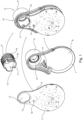
- FIG. 1 schematically illustrates various parts of an animal tag in accordance with an embodiment of the present invention.
- the animal tag 1 (see figure 2b for the numbering) includes a printed circuit board 5, a base part 7, and a coil holder 9. Assembled, prior to overmoulding in step 34 (e.g. figure 3 ), the various parts 5, 7 and 9 are illustrated in semi-manufacture part 19.
- the printed circuit board (PCB) 5 includes an attachment opening 12 that later forms the attachment opening of an ear tag 1.
- FIG. 1 , 2a and 2b illustrate an ear tag, the same manufacturing method may for example be applied for forming a neck tag, a tail tag, a leg tag or a stomach bolus.
- the example of an ear tag 1 is described here in order to illustrate the method of the present invention, although the invention is not limited to the manufacturing of ear tags alone, and may be applied to other type of animal sensor tags for use in livestock management systems.
- the attachment opening 12 is further present in the base part 7 as well as in the coil holder 9. In the semi-manufacture 19, the attachment opening 12 is likewise visible. As may be appreciated, the inner surface 17 of the coil holder 9 forms the inner surface 17 of the attachment opening 12 in the semi-manufacture 19. Again in figures 2a and 2b , the inner surface 17 of the coil holder 9 will likewise form an accessible surface 17 of the final ear tag 1.
- the printed circuit board 5 may include one or more mounting locations.
- the opening 16 in the printed circuit board 5 will correspond with an extending mounting element 15 on the base part 7.
- circumferential rim 14 of the attachment opening 12 in printed circuit board 5 will correspond to the outer surface of the edge 18 of the coil holder 9.
- the coil holder 9 may be placed into the attachment opening 12 of the printed circuit board, after which an antenna (not shown) can be wound around the coil holder 9.
- the grooves 10 in coil holder 9 provide guides for an antenna coil to be wound around the coil holder 9.
- the end of the extending parts 15 of the base part 7 can be seen to extend through the opening 16 in the printed circuit board 5.
- the fixation of edge 19 through the printed circuit board 5 can be seen in the semi-manufacture 19.
- the base part 7 comprises a housing part 8 that will in a later stage of the manufacturing process become part of the water resistant housing 25 ( figure 2b ) around the moulded interior part, as will be explained below. Furthermore, apart from interior surface 17 of the attachment opening 12, , in semi-manufacture 19 it can also be seen that the outer surface 6 of the base part 7 may likewise form a suitable fixation during the overmoulding steps (both accessible during the first overmoulding and the second overmoulding step) of the manufacturing method.
- base part 7 is an optional element to the animal tag 1 manufactured using a manufacturing method in accordance with an embodiment of the invention.
- Fixation may for example in both overmoulding steps be achieved through an attachment opening 12, which provides a commonly accessible fixation surface (such as internal surface 17) during both overmoulding steps.
- Figure 2a illustrates a semi-manufacture 21 of an ear tag 1 after the first moulding step has been completed.
- the internal surface 17 of attachment opening 12 as well as the other surface 6 of the base part 7 can be seen.
- the backside 23 of the semi-manufacture 21 the backside of the housing 8 visible in figure 1 will likewise be accessible, but may not always provide a good fixation location during the overmoulding step.
- the back side of housing 8 may optionally have been provided with surface structures, notches or indentations, which could provide suitable fixation points.
- fixation points 22 have been used in order to fix the printed circuit board 5 to the first mould (not visible).
- fixation may have been achieved by clamping the circumference 6 of the printed circuit board 5 visible in figure 1 .
- the shape of the clamps is still visible in figure 2a in the moulded interior part 20 obtained during the first moulding step.
- the ear tag 1 is illustrated resulting from the manufacturing method of the present invention. Still visible are the attachment opening 12 with its internal surface 17.
- the water resistant part 25 or water resistant water housing 25 is obtained by the second overmoulding step 40 of the present invention.
- the exterior base part 7 can be seen to be integrated into the water resistant part 25.
- the material from which the base part 7 is fabricated may be the same material used for performing the second overmoulding step 40.
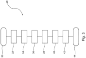
- FIG. 3 schematically illustrates a method in accordance with an embodiment of the present invention.
- the method 28 starts with optional preprocessing in step 30.
- the preprocessing step 30 may include for example the assembly of the various parts 5, 7 and 9 such as to form semi-manufacture 19 of figure 1 . If the base part 7 is absent, this may merely include the attachment of the printed circuit board 5 through the coil holder 9. In case of a neck tag or other kinds of tags, these could of course be other parts that are assembled in order to form a semi-manufacture.
- the semi-manufacture 19 may be fixed to the first mould for performing the first overmoulding step 34.
- fixation of the semi-manufacture 19 may include fixating the printed circuit board 5 to clamps or other holding part in the mould for performing the overmoulding step 34.
- the semi-manufacture 19 may be completely fixed by fixing the internal surface 17 of the attachment opening.
- a first step of overmoulding is carried out.
- the overmoulding is performed by casting, under pressure, a first polymer material into the mould wherein the PCB 5 recites.
- the first polymer material may be a polyamide hot melt which is characterized by having a relatively low viscosity at a temperature of 230 degrees Celsius.
- the viscosity may be less than 6.0 Pa s at a temperature of 240 degrees Celsius.
- the test to be performed may be standard test ASTM D3236. For example at an application temperature of 230 degrees Celsius the viscosity could be 3.0 to 4.0 Pa ⁇ s.
- step 36 the moulded interior part 20 obtained in step 34 is solidified.
- the solidifying step may for example have a duration of several hours to several days in order to achieve the desired hardness of the hot melt material.
- the hardness of the moulded interior part may for example be at least 30 Shore D, more preferably at least 40 Shore D at a temperature of 23.0 degrees Celsius. This can be determined in accordance with the standard test ISO868 for determination of indentation hardness by means of a durometer (Shore hardness) of plastics and ebonite.
- a suitable material that may be used may for example be a polyamide hold melt resin sold under the name Thermelt tm 195 natural, of Bostik S.A., la Plaine Saint-Denis France.
- Another suitable polyamide hot melt may for example be provided by the polyamide hot melt resin sold by Henkel AG & Co KGaA of Düsseldorf, Germany under the name Macromelt ® 2035S.
- the above mentioned materials are merely examples of suitable polyamide hot melt materials that may be used for producing the moulded interior part 20 of the present invention.
- the solidified moulded interior part 20 is fixed in a second mould in order to perform the second moulding step.
- the fixation location may be chosen to be internal to the attachment opening 12 in order to fix the semi-manufacture 21 to the second mould for performing the second overmoulding step.
- the second overmoulding is performed using a second polymer material.
- the second polymer material may be selected in order to provide a water resistant layer or a water resistant housing that encloses the moulded interior part 20.
- the moulded interior part 20 is thereby fully enclosed by the water resistant part 25, and thereby the electronics embedded in the moulded interior part 20, are fully protected against moist during their lifetime.
- Various suitable materials may be applied during the second overmoulding step 40, dependent on the properties desired. For example, for obtaining water resistancy various plastics such as Nylon tm (PA6), an acrylonitrile styrene acrylate (ASA), a polypropylene (PP), a polyethylene (PE), a polyoxymethylene (POM), polyvinylchloride (PVC), polystyrene (PS) may be considered.
- Nylon tm PA6
- ASA acrylonitrile styrene acrylate
- PP polypropylene
- PE polyethylene
- POM polyoxymethylene
- PVC polyvinylchloride
- PS polystyrene
- a second polymer material is a different material than the first polymer material, and may for example be provided by a plastic that provides a high level of water resistancy or may even be a different grade of a same or similar polymer that is already applied in the first overmoulding step 34.
- the temperatures applied in the overmoulding steps 34 and 40 may suitably be chosen dependent on the hot melt materials applied.
- the temperatures during this step 40 may be higher than the temperatures during step 34 for a limited amount of time. This, of course, is optional - the temperatures may also be selected to be lower during the second step 40 compared to the first step 34 if this is preferred dependent on the material applied during the second step 40.
- step 42 the water resistant part is solidified for several hours to several days in order to obtain the end product, an (operational) animal tag 1.
- various postprocessing steps may be applied, for example the imprinting of information on the tag or other postprocessing steps to the tag in step 44.
- additional steps may be added in order to provide certain functionality to the animal tag 1 or in order to improve various aspects of the manufacturing method described. This may be considered without departing from the claimed invention.
- various of the above mentioned methods may be optional, such as the preprocessing step 30 or the postprocessing step 44.
- any reference signs shall not be construed as limiting the claim.
- the term 'comprising' and 'including' when used in this description or the appended claims should not be construed in an exclusive or exhaustive sense but rather in an inclusive sense.
- the expression 'comprising' as used herein does not exclude the presence of other elements or steps in addition to those listed in any claim.
- the words 'a' and 'an' shall not be construed as limited to 'only one', but instead are used to mean 'at least one', and do not exclude a plurality.
- Features that are not specifically or explicitly described or claimed may be additionally included in the structure of the invention within its scope.
Landscapes
- Life Sciences & Earth Sciences (AREA)
- Engineering & Computer Science (AREA)
- Environmental Sciences (AREA)
- Biodiversity & Conservation Biology (AREA)
- Animal Husbandry (AREA)
- Manufacturing & Machinery (AREA)
- Microelectronics & Electronic Packaging (AREA)
- Mechanical Engineering (AREA)
- Birds (AREA)
- Zoology (AREA)
- Theoretical Computer Science (AREA)
- General Physics & Mathematics (AREA)
- Physics & Mathematics (AREA)
- Computer Hardware Design (AREA)
- Biophysics (AREA)
- Computer Networks & Wireless Communication (AREA)
- Radar Systems Or Details Thereof (AREA)
- Casting Or Compression Moulding Of Plastics Or The Like (AREA)
- Injection Moulding Of Plastics Or The Like (AREA)
Applications Claiming Priority (1)
| Application Number | Priority Date | Filing Date | Title |
|---|---|---|---|
| NL2034514A NL2034514B1 (en) | 2023-04-06 | 2023-04-06 | Method of manufacturing an animal tag, as well as animal tag. |
Publications (1)
| Publication Number | Publication Date |
|---|---|
| EP4442425A1 true EP4442425A1 (de) | 2024-10-09 |
Family
ID=86732901
Family Applications (1)
| Application Number | Title | Priority Date | Filing Date |
|---|---|---|---|
| EP24168540.3A Pending EP4442425A1 (de) | 2023-04-06 | 2024-04-04 | Verfahren zur herstellung eines tieretiketts sowie tieretikett |
Country Status (3)
| Country | Link |
|---|---|
| US (1) | US12387079B2 (de) |
| EP (1) | EP4442425A1 (de) |
| NL (1) | NL2034514B1 (de) |
Families Citing this family (1)
| Publication number | Priority date | Publication date | Assignee | Title |
|---|---|---|---|---|
| DE202022001554U1 (de) * | 2022-07-09 | 2022-11-02 | Biocv Gmbh | System zur Befestigung von elektronischen Einheiten am Ohr von Nutzieren |
Citations (3)
| Publication number | Priority date | Publication date | Assignee | Title |
|---|---|---|---|---|
| US7772979B2 (en) * | 2004-08-27 | 2010-08-10 | Reinhard Nehls | Ear tag element and methods for producing an ear tag element |
| FR2963722A1 (fr) * | 2010-08-13 | 2012-02-17 | Allflex Europ | Dispositif resine d'identification d'un animal, et procede de fabrication correspondant |
| AT13811U1 (de) * | 2014-01-16 | 2014-09-15 | Sapro Kunststoffverarbeitung Und Laserbeschriftungen E U | Ohrmarke zur Kennzeichnung und Identifizierung von Tieren |
Family Cites Families (6)
| Publication number | Priority date | Publication date | Assignee | Title |
|---|---|---|---|---|
| US20070137584A1 (en) * | 2005-12-16 | 2007-06-21 | Travis Bryan R | System for monitoring animal feed consumption |
| US7966971B2 (en) * | 2008-05-23 | 2011-06-28 | C-Lock Inc. | Method and system for monitoring and reducing ruminant methane production |
| US9256767B2 (en) * | 2009-11-11 | 2016-02-09 | Hand Held Products, Inc. | Tracking system |
| US10085419B2 (en) * | 2015-07-13 | 2018-10-02 | C-Lock Inc. | Modular livestock feed system for measuring animal intake and monitoring animal health |
| US11881287B2 (en) * | 2016-11-10 | 2024-01-23 | Precisionlife Ltd | Control apparatus and method for processing data inputs in computing devices therefore |
| WO2023113664A1 (en) * | 2021-12-16 | 2023-06-22 | Telefonaktiebolaget Lm Ericsson (Publ) | Techniques for tracing operations in a network |
-
2023
- 2023-04-06 NL NL2034514A patent/NL2034514B1/en active
-
2024
- 2024-04-04 US US18/626,476 patent/US12387079B2/en active Active
- 2024-04-04 EP EP24168540.3A patent/EP4442425A1/de active Pending
Patent Citations (3)
| Publication number | Priority date | Publication date | Assignee | Title |
|---|---|---|---|---|
| US7772979B2 (en) * | 2004-08-27 | 2010-08-10 | Reinhard Nehls | Ear tag element and methods for producing an ear tag element |
| FR2963722A1 (fr) * | 2010-08-13 | 2012-02-17 | Allflex Europ | Dispositif resine d'identification d'un animal, et procede de fabrication correspondant |
| AT13811U1 (de) * | 2014-01-16 | 2014-09-15 | Sapro Kunststoffverarbeitung Und Laserbeschriftungen E U | Ohrmarke zur Kennzeichnung und Identifizierung von Tieren |
Also Published As
| Publication number | Publication date |
|---|---|
| US12387079B2 (en) | 2025-08-12 |
| US20240338548A1 (en) | 2024-10-10 |
| NL2034514B1 (en) | 2024-10-14 |
Similar Documents
| Publication | Publication Date | Title |
|---|---|---|
| EP4442425A1 (de) | Verfahren zur herstellung eines tieretiketts sowie tieretikett | |
| KR100810937B1 (ko) | 온도 센서 | |
| JP5693237B2 (ja) | 磁界センサを製造する方法および装置 | |
| US7806587B2 (en) | Electronic clinical thermometer and method of producing the same | |
| US20120036930A1 (en) | Extrusion-coating method for a sensor device and sensor device | |
| JP6341508B2 (ja) | 防水コネクタ及び防水コネクタの製造方法 | |
| Zhang et al. | Mechanically matched silicone brain implants reduce brain foreign body response | |
| EP3226535A1 (de) | Bildaufnahmevorrichtung | |
| US11897215B2 (en) | Overmolded electronic eyewear device frame | |
| JP2007315873A (ja) | 電気装置およびその製造方法 | |
| CN1255646A (zh) | 制造光学组件的方法 | |
| US20200368948A1 (en) | Inner part and resin molded article | |
| WO2008051504A2 (en) | Rfid collar | |
| US20210252816A1 (en) | Manufacturing method of tire integrated electronic device | |
| SE452283B (sv) | Kulled samt sett att framstella denna | |
| JP5295583B2 (ja) | 埋設型ひずみ計 | |
| EP1487248B1 (de) | Halterungsstruktur und geformtes Teil mit dieser Halterungsstruktur | |
| US7703322B2 (en) | Liquid level detecting device and method of manufacturing same | |
| JP2005189080A (ja) | 温度センサー及びその製造方法 | |
| CN215826631U (zh) | 形成有集成电子器件的车辆内部装饰件 | |
| US20040190590A1 (en) | Apparatus for determining the temperature of a flowing medium in conduit and method for producing the apparatus | |
| JP2005109027A (ja) | 素子用筐体 | |
| US20040130070A1 (en) | Method and device for controlling the shrink behavior of plastic materials during primary shaping | |
| GB2239418A (en) | Fluid resin generates current used in assessment of curing thereof | |
| JP4390150B2 (ja) | 樹脂製軸受部品及びその製造方法 |
Legal Events
| Date | Code | Title | Description |
|---|---|---|---|
| PUAI | Public reference made under article 153(3) epc to a published international application that has entered the european phase |
Free format text: ORIGINAL CODE: 0009012 |
|
| STAA | Information on the status of an ep patent application or granted ep patent |
Free format text: STATUS: THE APPLICATION HAS BEEN PUBLISHED |
|
| AK | Designated contracting states |
Kind code of ref document: A1 Designated state(s): AL AT BE BG CH CY CZ DE DK EE ES FI FR GB GR HR HU IE IS IT LI LT LU LV MC ME MK MT NL NO PL PT RO RS SE SI SK SM TR |
|
| STAA | Information on the status of an ep patent application or granted ep patent |
Free format text: STATUS: REQUEST FOR EXAMINATION WAS MADE |
|
| 17P | Request for examination filed |
Effective date: 20250403 |