EP4446778A1 - Verbesserte lidar-bildgebungsvorrichtung - Google Patents
Verbesserte lidar-bildgebungsvorrichtung Download PDFInfo
- Publication number
- EP4446778A1 EP4446778A1 EP23305541.7A EP23305541A EP4446778A1 EP 4446778 A1 EP4446778 A1 EP 4446778A1 EP 23305541 A EP23305541 A EP 23305541A EP 4446778 A1 EP4446778 A1 EP 4446778A1
- Authority
- EP
- European Patent Office
- Prior art keywords
- incident
- metalens
- lidar device
- metalenses
- laser beam
- Prior art date
- Legal status (The legal status is an assumption and is not a legal conclusion. Google has not performed a legal analysis and makes no representation as to the accuracy of the status listed.)
- Pending
Links
Images




Classifications
-
- G—PHYSICS
- G01—MEASURING; TESTING
- G01S—RADIO DIRECTION-FINDING; RADIO NAVIGATION; DETERMINING DISTANCE OR VELOCITY BY USE OF RADIO WAVES; LOCATING OR PRESENCE-DETECTING BY USE OF THE REFLECTION OR RERADIATION OF RADIO WAVES; ANALOGOUS ARRANGEMENTS USING OTHER WAVES
- G01S17/00—Systems using the reflection or reradiation of electromagnetic waves other than radio waves, e.g. lidar systems
- G01S17/02—Systems using the reflection of electromagnetic waves other than radio waves
- G01S17/06—Systems determining position data of a target
- G01S17/42—Simultaneous measurement of distance and other co-ordinates
-
- G—PHYSICS
- G01—MEASURING; TESTING
- G01S—RADIO DIRECTION-FINDING; RADIO NAVIGATION; DETERMINING DISTANCE OR VELOCITY BY USE OF RADIO WAVES; LOCATING OR PRESENCE-DETECTING BY USE OF THE REFLECTION OR RERADIATION OF RADIO WAVES; ANALOGOUS ARRANGEMENTS USING OTHER WAVES
- G01S17/00—Systems using the reflection or reradiation of electromagnetic waves other than radio waves, e.g. lidar systems
- G01S17/88—Lidar systems specially adapted for specific applications
- G01S17/89—Lidar systems specially adapted for specific applications for mapping or imaging
-
- G—PHYSICS
- G01—MEASURING; TESTING
- G01S—RADIO DIRECTION-FINDING; RADIO NAVIGATION; DETERMINING DISTANCE OR VELOCITY BY USE OF RADIO WAVES; LOCATING OR PRESENCE-DETECTING BY USE OF THE REFLECTION OR RERADIATION OF RADIO WAVES; ANALOGOUS ARRANGEMENTS USING OTHER WAVES
- G01S7/00—Details of systems according to groups G01S13/00, G01S15/00, G01S17/00
- G01S7/48—Details of systems according to groups G01S13/00, G01S15/00, G01S17/00 of systems according to group G01S17/00
- G01S7/481—Constructional features, e.g. arrangements of optical elements
- G01S7/4816—Constructional features, e.g. arrangements of optical elements of receivers alone
-
- G—PHYSICS
- G01—MEASURING; TESTING
- G01S—RADIO DIRECTION-FINDING; RADIO NAVIGATION; DETERMINING DISTANCE OR VELOCITY BY USE OF RADIO WAVES; LOCATING OR PRESENCE-DETECTING BY USE OF THE REFLECTION OR RERADIATION OF RADIO WAVES; ANALOGOUS ARRANGEMENTS USING OTHER WAVES
- G01S7/00—Details of systems according to groups G01S13/00, G01S15/00, G01S17/00
- G01S7/48—Details of systems according to groups G01S13/00, G01S15/00, G01S17/00 of systems according to group G01S17/00
- G01S7/481—Constructional features, e.g. arrangements of optical elements
- G01S7/4817—Constructional features, e.g. arrangements of optical elements relating to scanning
-
- G—PHYSICS
- G01—MEASURING; TESTING
- G01S—RADIO DIRECTION-FINDING; RADIO NAVIGATION; DETERMINING DISTANCE OR VELOCITY BY USE OF RADIO WAVES; LOCATING OR PRESENCE-DETECTING BY USE OF THE REFLECTION OR RERADIATION OF RADIO WAVES; ANALOGOUS ARRANGEMENTS USING OTHER WAVES
- G01S7/00—Details of systems according to groups G01S13/00, G01S15/00, G01S17/00
- G01S7/48—Details of systems according to groups G01S13/00, G01S15/00, G01S17/00 of systems according to group G01S17/00
- G01S7/483—Details of pulse systems
- G01S7/486—Receivers
- G01S7/4865—Time delay measurement, e.g. time-of-flight measurement, time of arrival measurement or determining the exact position of a peak
-
- G—PHYSICS
- G02—OPTICS
- G02B—OPTICAL ELEMENTS, SYSTEMS OR APPARATUS
- G02B1/00—Optical elements characterised by the material of which they are made; Optical coatings for optical elements
- G02B1/002—Optical elements characterised by the material of which they are made; Optical coatings for optical elements made of materials engineered to provide properties not available in nature, e.g. metamaterials
-
- G—PHYSICS
- G02—OPTICS
- G02B—OPTICAL ELEMENTS, SYSTEMS OR APPARATUS
- G02B3/00—Simple or compound lenses
- G02B3/0006—Arrays
- G02B3/0037—Arrays characterized by the distribution or form of lenses
- G02B3/0056—Arrays characterized by the distribution or form of lenses arranged along two different directions in a plane, e.g. honeycomb arrangement of lenses
-
- G—PHYSICS
- G02—OPTICS
- G02F—OPTICAL DEVICES OR ARRANGEMENTS FOR THE CONTROL OF LIGHT BY MODIFICATION OF THE OPTICAL PROPERTIES OF THE MEDIA OF THE ELEMENTS INVOLVED THEREIN; NON-LINEAR OPTICS; FREQUENCY-CHANGING OF LIGHT; OPTICAL LOGIC ELEMENTS; OPTICAL ANALOGUE/DIGITAL CONVERTERS
- G02F1/00—Devices or arrangements for the control of the intensity, colour, phase, polarisation or direction of light arriving from an independent light source, e.g. switching, gating or modulating; Non-linear optics
- G02F1/29—Devices or arrangements for the control of the intensity, colour, phase, polarisation or direction of light arriving from an independent light source, e.g. switching, gating or modulating; Non-linear optics for the control of the position or the direction of light beams, i.e. deflection
- G02F1/292—Devices or arrangements for the control of the intensity, colour, phase, polarisation or direction of light arriving from an independent light source, e.g. switching, gating or modulating; Non-linear optics for the control of the position or the direction of light beams, i.e. deflection by controlled diffraction or phased-array beam steering
Definitions
- the present invention concerns LIDAR imaging device and more precisely LIDAR imaging device based on Time Of Flight measurements.
- a category of LIDAR systems employs pulses of light to measure the distance to an object based on the time of flight (TOF) of each pulse of light and possibly the velocity of this object. A portion of the light reflects from the object and returns to a detector of the LIDAR system. Based on the time elapsed between emission of the pulse of light and detection of the returned pulse of light, a distance is estimated.
- TOF time of flight
- LIDAR systems require the scanning of space with an optical beam to achieve a two- or three-dimensional detection of the observed scene. In general, this involves scanning the space with an optical beam. This results in a scanning time that may be detrimental to some applications. While the beam is directed towards a given direction, other directions in the scene are not observed. Furthermore, the area covered by the LIDAR and the speed of its coverage depend on the solutions chosen to build the LIDAR.
- the distance covered by the LIDAR which is proportional to the power of the laser used
- the solid angle covered by the LIDAR which depends on the type of application (surveillance or escort, for example)
- the speed with which the LIDAR probes the area covered which generally depends on the type and speed of the targets sought.
- the first solution is mechanical. It consists of using a pair of laser transmitter and receiver which both point in the same direction.
- the assembly is mobile in order to scan the space. It may also involve one or more movable mirrors that allow the light beam from the laser transmitter to be directed and the reflected signal to be directed onto the photodetector.
- These scanning devices can eventually be miniaturized using optical MEMS (microelectromechanical systems). While this solution has the advantage of not depending on the wavelength used for LIDAR, it requires precise alignment of the optical system, and is very sensitive to vibration and acceleration, which severely limits the possible applications.
- the second solution consists in using an interferential optical system to deflect the optical beam.
- the principle is to use an optical interference arrangement to direct the light in a given direction in space as a function of wavelength. In general, this involves separating the optical signal into several points and imposing a phase shift between these points. The interference between the signals from these points is constructive in a given direction. By varying the phase shift between these points, either by using phase modulators or by varying the wavelength of the laser used, the system scans the direction pointed by the optical beam.
- This solution has the advantage of not relying on any moving parts but imposes certain constraints on the speed of laser tuning and its reproducibility.
- the third solution consists in generating a point cloud illumination and detecting a 3D image using multiple detectors or an array of detectors to sample the signal and further measure the TOF for each pixel of the detector.
- the light path of a single laser emitter/detector combination is somehow altered to achieve a broader field of view than a single sensor.
- the number of pixels such devices can generate per unit time is inherently limited due limitations on the pulse repetition rate of a single laser. Any alteration of the beam path, whether it is by mirror, prism, or actuation of the device that achieves a larger coverage area comes at a cost of decreased point cloud density.
- a sequence of pulses is emitted.
- the direction of each pulse is sequentially varied in rapid succession.
- a distance measurement associated with each individual pulse can be considered a pixel, and a collection of pixels emitted and captured in rapid succession (i.e., "3D point cloud”) can be rendered as an image or analyzed for other reasons (e.g., detecting obstacles).
- viewing software is employed to render the resulting point clouds as images that appear three dimensional to a user. Different schemes can be used to depict the distance measurements as 3D images that appear as if they were captured by a live action camera.
- each of the multiple pulses is projected in a different direction.
- each volume of space interrogated by each of the multiple pulses is completely separated from any volume of space interrogated by any of the other multiple pulses. As the separation among simultaneously interrogated spaces is increased, the likelihood of inducing measurement error due to cross-talk is reduced.
- an object of the invention is a LIDAR imaging device that comprises an array of N > 1 metalenses each adapted to collect a respective portion, called a sub-beam, of a laser beam reflected by the observed environment.
- Each metalens is a metasurface adapted to focus a respective sub-beam of the reflected illumination onto a respective pixel of a photodetector only when said respective sub beam is incident onto said metalens within a predetermined range of incident angles centered on a respective pair of optimal incident angle, different from and not overlapping with the predetermined ranges of optimal incident angle associated to other metalenses.
- the LIDAR imaging device of the invention has an important FOV and has a greater working distance than flash LIDAR devices of the prior art.
- An object of the invention is a LIDAR device to image a three dimensional environment comprising :
- the processing unit is configured to determine a time of flight of the sub-beam detected by the photodetector.
- the photodetectors and the metalenses are adapted such that the reflected laser beam incident onto the array of metalenses within one of said predetermined ranges of incident angles [ ⁇ ⁇ i , ⁇ ⁇ i ] is focused only onto the respective pixel P i associated to said predetermined range of incident angles [ ⁇ ⁇ i , ⁇ ⁇ i ].
- each metalens comprises nanostructures arranged in a periodic grating on a substrate.
- each nanostructure presents an aspect ratio H / w greater or equal to 2, preferably greater or equal to 10, with H a height and w a width of said nanostructures, said height H being greater than said wavelength ⁇ .
- each nanostructure presents a circular symmetry preferably a cylindric shape or a conic shape.
- the nanostructures present a height H comprised between 500 nm and 5 ⁇ m and a width comprised between 15 nm and 250 nm.
- each nanostructure is a metallic nanoparticle with a diameter comprised between ⁇ /15 and ⁇ /5.
- n t and n i are respectively the refractive indexes of a transmitted and an incident medium with respect to said metalens
- f is a focal length of the metalens
- k i is a normalized incident wave vector of the respective sub beam incident onto said metalens with said pair of optimal incident angle.
- the number N of metalenses, a spatial arrangement of the metalenses within said array and a diameter of each metalens are adapted such that a total field of view of said LIDAR device is greater than 90 ° ⁇ 90 ° , preferably greater or equal to 120 ° ⁇ 120 ° .
- each metalens has a hexagonal shape, and wherein the metalenses are arranged side by side such that the array of metalenses has a hexagonal shape.
- each metalens is adapted such that its associated predetermined range of incident angles has a width comprised between 1° and 10°.
- the laser source is a pulsed laser source such that said incident laser beam presents a plurality of laser pulses, and wherein the scanning element is synchronized with the laser source to induce a controllable shift of a direction of propagation of said incident laser beam for each laser pulses.
- each diffraction region is designed by conventional diffraction consideration and/or using an inverse problem reconstruction algorithm, for example the Gerchberg-Saxton algorithm, such that it generates said respective point with identical intensity for each direction.
- the processing unit is adapted to compute an image that is the concatenation of each image acquired for each controllable shift induced by the scanning element.
- Figure 1 illustrates a LIDAR device 1 according to a first embodiment of the invention and adapted to image a three-dimensional environment (referenced Obj in figure 1 ).
- the LIDAR device 1 comprises a laser source SL, a scanning element SE, an array AM of N > 1 metalenses ML 1- ML N , a photodetector DT and a processing unit PU.
- the laser source SL is adapted to emit an incident laser beam LI presenting a wavelength ⁇ to illuminate the three-dimensional environment Obj.
- the incident laser beam LI reflected by the environment is hereinafter called reflected laser beam LR.
- the laser source SL is not specific to the present invention and can be any laser source known to one skilled in the art, for example a laser diode.
- the laser source SL is preferably a pulsed laser source to facilitate the TOF measurements of the observed environment.
- the laser source SL is a continuous source adapted such that the incident laser beam LI presents an intensity modulation or frequency modulation.
- the scanning element SE is adapted to induce a plurality of controllable shifts of a direction of propagation of the incident laser beam LI onto said three-dimensional environment.
- the scanning element SE comprises a pair of galvanometer scanning mirrors.
- an angle shift applied to the mirrors induces a shift of the direction of propagation of the incident laser beam LI.
- the processing unit PU is connected to the scanning element SE, to the laser source SL and to the detector DT for synchronization.
- the scanning element SE induces a controllable shift of a direction of propagation of said incident laser beam LI for each laser pulses emitted (or for each modulation period) to reconstruct a large field of view image of the observed environment Obj.
- the scanning element can be controlled via the processing unit PU to realize a raster scan or random scan of the observed environment Obj.
- the array AM comprises N metalenses noted ML 1 to ML N .
- the design and the performance of the metalenses will be discussed further below, in the description of the figures 2A to 8 .
- the photodetector is typically a CCD, CMOS camera, a SPAD (Single Photon Avalanche Diode) array, a APD (avalanche photo-detector), a MPPC (muti-pixel photon counters) or an array of photomultiplier tubes.
- each metalens comprises nanostructures NS with a structure adapted such that a sub-beam propagating with a given direction of propagation can only be focused onto one predetermined pixel of the photodetector DT.
- a structure adapted it is meant that the refraction index, the dimensions and the spatial arrangement of the nanostructures of each metalens are optimized with respect to the wavelength ⁇ to achieve the aforementioned result.
- the nanostructures are optimized using a FDTD ( Finite Difference Time Domain ) simulation software, for example Lumerical or any other software dedicated to nanophotonics.
- the metalenses are optimized for a given geometry of the detector DT to match the numerical aperture, pixel size and the spatial distribution of the underlying detector array to achieve the aforementioned result.
- This predetermined range ( ⁇ ⁇ i , ⁇ ⁇ i ) of incident angles is centered on a pair of optimal incident angle ( ⁇ opt,i ; ⁇ opt,i ) which corresponds to the predetermined direction which the metalens ML i is specifically adapted to focus onto its respective pixel P i .
- the processing unit PU is connected to the photodetector and is configured to acquire an image with the photodetector for each controllable shift induced by the scanning element. By merging the images taken for each controllable shift induced, the processing unit PU can then reconstruct a large field of view image of the observed scene. This merging may be done by a simple concatenation of each image acquired for each controllable shift induced by the scanning element.
- the processing unit is also configured to determine a time of flight of each sub-beam detected by the photodetector from its emission by the laser source to its detection by the photodetector. From this time of flight measurement, the processor is then configured to determine the distance of the object(s) in the observed environment that reflected the incident beam LI.
- the LIDAR imaging device 1 of the invention has an important FOV and can have a greater working distance than flash LIDAR devices of the prior art when used with a diffractive optical element to generate point cloud illuminations (see figure 9 described below). Further, it makes the LIDAR device 1 more compact than prior art LIDAR devices using metalenses to focus the reflected illumination onto the photodetector.
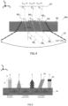
- Figure 2A and 2B are schematic representations of a side view and a front view respectively of a metalens ML i of the array AM according an embodiment of the invention.
- FIGS 2A and 2B are represented a sub beam SB i with a wavevector k i that is incident onto the metalens with the optimal incident angles ( ⁇ ; ⁇ ) associated with the metalens ML i .
- n t and n i are respectively the refractive indexes of a transmitted and an incident medium with respect to said metalens
- f is a focal length of the metalens
- k i is the normalized incident wave vector of the sub beam incident onto the metalens ML i with the pair of optimal incident angle ( ⁇ opt,i ; ⁇ opt,i ) associated with the metalens ML i .
- Any other focusing like phase profile including quadratic or Bessel phase profile to which directionality phase information can be added and that renders the focusing directional can be considered.
- phase profile of the metalens must ensure that each metalens can collect light in its own direction in space (defined by the pair of optimal incident angle ( ⁇ opt,i ; ⁇ opt,i )).
- ⁇ opt,i the pair of optimal incident angle
- the transmission is defined as the ratio of the two-dimensional integral of the Poynting vector just after the metasurface and the two-dimensional integral of the Poynting vector of the sub-beam.
- the two-dimensional integrals are performed on a surface corresponding to the area of the metalens.
- the spot efficiency is the ratio between the 2D integral of the Poynting vector just after the metasurface (integrated on the hexagonal metasurface area) and the 2D integral of the Poynting vector in the focal plane (integrated on the pixel area).
- the hexagonal shape does not deteriorate the functionality of the metalens. Indeed, the two shapes of metalens have the same transmission (dash-dot lines) greater than 70% for ⁇ ⁇ 15°. On the other hand, for an illumination at normal incidence, the spot efficiency (dashed lines) is slightly higher for the hexagonal metalens by a few percent.
- the metalenses of the invention act either as on or off-axis Fresnel lenses to focus the sub beams onto their respective pixels.
- the central metalens designed for zero incident angle has transmission and the phase profile presenting a radial symmetry.
- the phase profiles are composed of a focusing and a directional contributions.
- the metalenses comprises nanostructures NS arranged in a periodic grating on a substrate SB.
- the spatial period of the grating must be at least two times less than the wavelength ⁇ of the incident laser beam LI.
- the substrate is made of sapphire or silica and the nanostructures are made of GaN or silicon.
- the choice of the material is preferably adapted to the target wavelength of the laser source.
- the figure 4 is a schematic illustration of a side view of the array AM of metalenses and the photodetector DT.
- three metalenses ML 1 , ML 2 and ML 3 , their respective sub-beams SB 1 , SB 2 and SB 3 , and their associated pixels P 1 , P 2 and P 3 are represented in figure 4 .
- the refraction of the light on this first interface reduces the field of view compared to the field of view in air. Therefore, because of the substrate SB, the metalenses are optimized based on the refracted angles and not on the illumination angles ⁇ ill and ⁇ ill .
- the reflected beam LR passes through a first air-substrate interface before illuminating the metalenses.
- Each metalenses then focuses its respective sub-beam.
- the metalens ML 1 is the only metalens that focuses its respective sub beam SB 1 onto its associated pixel P 1 .
- the other metalenses ML 2 , ML 3 focus their respective sub-beams SB 1 , SB 2 outside of the detection zone of their associated pixels P 2 and P 3 .
- the field of view (FOV) of the device 1 is intrinsically limited by the transverse dimensions of the array AM (i.e. the dimensions in the xy plane comprising the AM array). Indeed, one can always adapt the photodetector DT to the transverse dimensions of the array AM.
- the transverse dimensions of the array AM are dependent upon the number N of metalenses, the spatial arrangement of the metalenses within the array AM, the dimensions and the orientation of each metalens.
- dimensions of each metalens it is meant the transverse dimensions of the metalens, in the plane of the array AM.
- each metalens has a hexagonal shape and the metalenses are arranged side by side such that the array of metalenses has an hexagonal shape.
- the array comprises metalenses with a hexagonal shape and metalenses with a pentagonal shape to sample the discretized FOV in a more optimal manner.
- the FOV is approximated by a portion of polyhedron made of 310 hexagons and 6 pentagons and is sampled by an array AM of 316 hexagonal metalenses arranged edge to edge on an hexagonal array.
- each metalens has a maximal transverse dimension of 23 ⁇ m.
- the LIDAR device comprises a non-periodic detector DT and the array AM comprises metalenses with a non-unique geometry.
- the photodetector DT comprises a matrix of pixels with increasing distance between pixels and the array AM comprises metalenses with a top metasurface layer of increasing diameter. This configuration can help increase the dimension of the collection area and can improve the detection of sub-beams with high incidence angles. Thus, one can improve the signal to noise ratio of the pixels associated with those sub-beams.
- diameter it is meant the maximal transverse dimension of the metalens.
- an optimal structure of the metalenses is one that comprises nanostructures presenting an aspect ratio H / w greater or equal to 2, preferably greater or equal to 10, with H a height and w a width of the nanostructures.
- the height H of the nanostructures NS is greater than the wavelength ⁇ of the incident laser beam LI.
- the nanostructures are designed with appropriate dimensions such that the array of metalenses can achieve a full phase modulation of 2 ⁇ of the collected light.
- the maximal dimension of the nanostructures it is meant the maximal dimension of the nanostructures along the direction perpendicular to the array AM (i.e. the direction z according to the illustrated examples).
- width it is meant the maximal dimension of the nanostructures along a direction parallel to the array AM (i.e., the direction x or y according to the illustrated examples).
- Figure 5 illustrates five different configurations of nanostructures NS that may be used in the metalenses of the invention. Those shapes are given as a non-limiting example and one skilled in the art can easily depart from those shapes to implement the invention.
- the nanostructures NS may comprise an antireflection layer AR deposited on top of the nanostructure to enhanced the transmission of the metalens.
- a layer is optically transparent to the illumination wavelength ⁇ and presents a thickness (dimension along the direction z ) equal to ⁇ /4.
- each nanostructure presents a circular symmetry (also called axial symmetry or revolution symmetry).
- the metalens have a polarization independent behavior.
- the metalenses comprise nanostructures presenting a height H comprised between 500 nm and 5 ⁇ m and a width comprised between 15 nm and 250 nm.
- each nanostructure is a metallic nanoparticle with a diameter comprised between ⁇ /15 and ⁇ /5.
- these nanoparticles are less efficient to focus the sub-beams than the nanostructures illustrated in figure 5 , they are quite efficient for wavelength in the THz range and the micro-wave range.
- each metalens ML is a Pancharatnam-Berry (PB) metasurface.
- PB metasurface is known in the art (see e.g. Gao, Zhanjie, Golla, Sandeep, Sawant, Rajath, Osipov, Vladimir, Briere, Gauthier, Dunan, Stephane, Damilano, Benjamin, Genevet, Patrice and Dorfman, Konstantin E.. "Revealing topological phase in Pancharatnam-Berry metasurfaces using mesoscopic electrodynamics" Nanophotonics, vol. 9, no. 16, 2020, pp. 4711-4718.
- the array AM can achieve a full phase modulation of 2 ⁇ of the collected light by the appropriate orientation of each PB metalens with respect to the other metalenses.
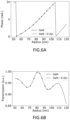
- the non-dotted line in figures 6A and 6B correspond to a range of radius for which a 2 ⁇ phase modulation is reached, and the points on the curves correspond to the radii that map the 2 ⁇ phase modulation in ⁇ /12 steps.
- the metasurfaces are composed of several GaN cylinders disposed according to the agreement between their respective phase (and amplitude) profile with the desired phase profile.
- phase response of a single nanopillar of the illustrative embodiment can produce a full-phase modulation (2 ⁇ phase shift) with a high transmission coefficient (higher than 90%) of the focused sub-beam.
- each pixel has a dimension of 5 ⁇ m along the x axis and each metalens is adapted map the field of view in angular steps of 6.66° in ⁇ and in 7.5° in ⁇ .
- the gray dotted line area corresponds to the size of the pixel associated with the metalens.
- the extreme values of the grayscale are the maximum and minimum intensities of the field map at normal incidence.
- the top portion a) of figure 8 illustrates the evolution of the phase profile as the oblique optimal detection angle ⁇ opt increases.
- the bottom left portion b) is a graph representing the evolution of the spot efficiency, as a function of the angle of incidence ⁇ , of a set of ten different metalenses optimized for different optimal incident angle comprising the aforementioned four metalenses.
- the bottom right graph c) represents the evolution of the transmission as a function of the angle of incidence ⁇ of the same set of ten different metalenses.
- portion a) of figure 8 one can see that to focus the light coming from an increasingly oblique direction, it is necessary to shift and deform more and more the center of the phase profile.
- the photodetector may need to be optimized so that one direction of the reflected beam LR can only be focused onto one pixel of the photodetector DT.
- the processing unit may be configured to integrate the field intensity on a smaller number of pixels to artificially reduce the detection area and avoid crosstalk between pixels.
- the photodetector DT is a matrix of physical detectors (e.g. SPADs)
- the photodetector DT may comprise a mask (e.g. a gold mask).
- this mask comprises circular holes smaller than the dimensions of the physical detectors and disposed optically upstream of the physical detectors to mechanically reduce the detection area and thus reduce the crosstalk between pixels.
- FIG 9 is a schematic illustration of a LIDAR device 1 according to a second embodiment of the invention.
- the LIDAR device 1 according to the second embodiment of the invention figure differs from the first embodiment of the invention illustrated in figure 1 in that it comprises a diffractive optical element DOE thus making the device 1 a flash LIDAR device.
- the diffractive optical element comprises M > 1 diffraction regions DR 1 - DR M .
- Each diffraction region is adapted to generate a respective point cloud with diffraction directions that preferably do not overlap with diffraction directions of the point cloud of the other diffraction regions.
- the scanning element SE is adapted to scan the different diffraction regions of the diffraction optical element DOE.
- the scanning element is adapted to such that the incident laser beam LI illuminates successively each diffraction region.
- the diffraction optical element DOE generates a points cloud to compute the source-object distance simultaneously in several directions and the processing unit can reconstruct a complete image of the observed environment faster than the first embodiment of the invention. Indeed, the generation of point clouds reduces the number of scanning steps necessary to fully reconstruct the FOV.
- the diffraction regions are metasurfaces designed using an inverse reconstruction algorithm.
- the phase profile of each diffraction region is designed to produce a predetermined point cloud using the Gerchberg-Saxton (GS) algorithm or a modified Gerchberg-Saxton algorithm.
- This algorithm determines a phase profile that generates a far field diffraction pattern. To do this, it performs a cycles of Fourier transform and inverse Fourier transform to switch iteratively between the plane of the diffractive optical element DOE and the far field plane and, for each iteration, changes the intensity or phase of the complex wave.
- the far-field image is a point cloud whose distribution counterbalances the Barrel distortion that occurs during the wave propagation.
- Another advantage of this design method is that it can produce diffraction regions which generate a points cloud with identical intensity for each direction. This is a stark contrast compared to conventional diffraction methods (i.e. gratings) where the intensity decreases as the diffraction order increases. For this, one adjusts the intensity of the light spots on the far field images used in the GS algorithm.
- conventional diffraction methods i.e. gratings
- each diffraction region is designed using an inverse problem reconstruction algorithm such that it generates said respective point with identical intensity for each direction using a far field image of the diffraction pattern produced by said diffraction region.
- the inventors estimated that it is preferable that the diffraction optical element DOE comprises at least 10 diffraction regions, each diffraction region generating at least 200 diffraction directions.
- the diffraction optical element DOE comprises less than 50 diffraction regions, each diffraction region generating less than 500 diffraction directions More precisely, it is preferable that the number of diffraction directions must be less than or equal to the number of metalenses. Limiting the number of diffraction directions helps increasing the working distance of the LIDAR device.
- the diffraction optical element DOE comprises 19 diffraction regions is sufficient, each diffraction region generating 316 diffraction directions.
- the laser source SL is a pulsed laser source and the scanning element is synchronized with the laser source such that each laser pulse illuminates a diffraction region that is different from a diffraction region illuminated by the previous pulse.
Landscapes
- Physics & Mathematics (AREA)
- Engineering & Computer Science (AREA)
- General Physics & Mathematics (AREA)
- Computer Networks & Wireless Communication (AREA)
- Radar, Positioning & Navigation (AREA)
- Remote Sensing (AREA)
- Electromagnetism (AREA)
- Optics & Photonics (AREA)
- Nonlinear Science (AREA)
- Optical Radar Systems And Details Thereof (AREA)
Priority Applications (3)
| Application Number | Priority Date | Filing Date | Title |
|---|---|---|---|
| EP23305541.7A EP4446778A1 (de) | 2023-04-12 | 2023-04-12 | Verbesserte lidar-bildgebungsvorrichtung |
| KR1020257035777A KR20250172824A (ko) | 2023-04-12 | 2024-04-11 | 개선된 라이다 이미징 장치 |
| PCT/EP2024/059829 WO2024213633A1 (en) | 2023-04-12 | 2024-04-11 | Improved lidar imaging device |
Applications Claiming Priority (1)
| Application Number | Priority Date | Filing Date | Title |
|---|---|---|---|
| EP23305541.7A EP4446778A1 (de) | 2023-04-12 | 2023-04-12 | Verbesserte lidar-bildgebungsvorrichtung |
Publications (1)
| Publication Number | Publication Date |
|---|---|
| EP4446778A1 true EP4446778A1 (de) | 2024-10-16 |
Family
ID=86903995
Family Applications (1)
| Application Number | Title | Priority Date | Filing Date |
|---|---|---|---|
| EP23305541.7A Pending EP4446778A1 (de) | 2023-04-12 | 2023-04-12 | Verbesserte lidar-bildgebungsvorrichtung |
Country Status (3)
| Country | Link |
|---|---|
| EP (1) | EP4446778A1 (de) |
| KR (1) | KR20250172824A (de) |
| WO (1) | WO2024213633A1 (de) |
Citations (7)
| Publication number | Priority date | Publication date | Assignee | Title |
|---|---|---|---|---|
| DE102015110767A1 (de) * | 2015-07-03 | 2017-01-05 | Valeo Schalter Und Sensoren Gmbh | Detektoreinheit für eine optische Sensorvorrichtung |
| DE102015225863A1 (de) | 2015-12-18 | 2017-06-22 | Robert Bosch Gmbh | Optische phasengesteuerte Anordnung und LiDAR System |
| WO2017132704A1 (en) | 2016-01-31 | 2017-08-03 | Velodyne Lidar, Inc. | Lidar based 3-d imaging with far-field illumination overlap |
| US20170269215A1 (en) | 2016-03-19 | 2017-09-21 | Velodyne Lidar, Inc. | Integrated Illumination And Detection For LIDAR Based 3-D Imaging |
| US20180052378A1 (en) | 2016-08-17 | 2018-02-22 | Samsung Electronics Co., Ltd. | Optical phased array (opa) |
| EP3457179A1 (de) * | 2017-09-13 | 2019-03-20 | Samsung Electronics Co., Ltd. | Lidar-vorrichtung und betriebsverfahren dafür |
| WO2022174120A1 (en) * | 2021-02-12 | 2022-08-18 | The Regents Of The University Of California | Metasurface, metalens, and metalens array with controllable angular field-of-view |
-
2023
- 2023-04-12 EP EP23305541.7A patent/EP4446778A1/de active Pending
-
2024
- 2024-04-11 WO PCT/EP2024/059829 patent/WO2024213633A1/en not_active Ceased
- 2024-04-11 KR KR1020257035777A patent/KR20250172824A/ko active Pending
Patent Citations (7)
| Publication number | Priority date | Publication date | Assignee | Title |
|---|---|---|---|---|
| DE102015110767A1 (de) * | 2015-07-03 | 2017-01-05 | Valeo Schalter Und Sensoren Gmbh | Detektoreinheit für eine optische Sensorvorrichtung |
| DE102015225863A1 (de) | 2015-12-18 | 2017-06-22 | Robert Bosch Gmbh | Optische phasengesteuerte Anordnung und LiDAR System |
| WO2017132704A1 (en) | 2016-01-31 | 2017-08-03 | Velodyne Lidar, Inc. | Lidar based 3-d imaging with far-field illumination overlap |
| US20170269215A1 (en) | 2016-03-19 | 2017-09-21 | Velodyne Lidar, Inc. | Integrated Illumination And Detection For LIDAR Based 3-D Imaging |
| US20180052378A1 (en) | 2016-08-17 | 2018-02-22 | Samsung Electronics Co., Ltd. | Optical phased array (opa) |
| EP3457179A1 (de) * | 2017-09-13 | 2019-03-20 | Samsung Electronics Co., Ltd. | Lidar-vorrichtung und betriebsverfahren dafür |
| WO2022174120A1 (en) * | 2021-02-12 | 2022-08-18 | The Regents Of The University Of California | Metasurface, metalens, and metalens array with controllable angular field-of-view |
Non-Patent Citations (1)
| Title |
|---|
| GAO, ZHANJIEGOLLA, SANDEEPSAWANT, RAJATHOSIPOV, VLADIMIRBRIERE, GAUTHIERVEZIAN, STEPHANEDAMILANO, BENJAMINGENEVET, PATRICEDORFMAN,: "Revealing topological phase in Pancharatnam-Berry metasurfaces using mesoscopic electrodynamics", NANOPHOTONICS, vol. 9, no. 16, 2020, pages 4711 - 4718 |
Also Published As
| Publication number | Publication date |
|---|---|
| WO2024213633A1 (en) | 2024-10-17 |
| KR20250172824A (ko) | 2025-12-09 |
Similar Documents
| Publication | Publication Date | Title |
|---|---|---|
| US12461206B2 (en) | LIDAR receiver using a waveguide and an aperture | |
| US11619718B2 (en) | Integrated optical structures for LiDAR and other applications employing multiple detectors | |
| CN109557522B (zh) | 多射束激光扫描仪 | |
| EP3529571B1 (de) | Anordnung aus wellenleiterdiffusoren zur lichtdetektion mit einer apertur | |
| CN110824490B (zh) | 一种动态距离测量系统及方法 | |
| JP7019894B2 (ja) | 物体を感知する方法及びセンサシステム | |
| TWI838490B (zh) | 基於飛行時間的三維感測系統 | |
| US11940263B2 (en) | Detector for determining a position of at least one object | |
| US20190137611A1 (en) | Scanning optical beam source | |
| US11561284B2 (en) | Parallax compensating spatial filters | |
| US12535563B2 (en) | Coaxial lidar system using a diffractive waveguide | |
| CN115136025B (zh) | 一种激光探测系统及车辆 | |
| US11156716B1 (en) | Hybrid LADAR with co-planar scanning and imaging field-of-view | |
| Majorel et al. | Bio-inspired flat optics for directional 3D light detection and ranging | |
| EP4446778A1 (de) | Verbesserte lidar-bildgebungsvorrichtung | |
| CN110456327B (zh) | 激光雷达接收装置及激光雷达系统 | |
| EP4307005A1 (de) | Detektionsvorrichtung | |
| US12123950B2 (en) | Hybrid LADAR with co-planar scanning and imaging field-of-view | |
| US11372109B1 (en) | Lidar with non-circular spatial filtering | |
| WO2024024745A1 (ja) | 測定装置、受光器、及び投光器 |
Legal Events
| Date | Code | Title | Description |
|---|---|---|---|
| PUAI | Public reference made under article 153(3) epc to a published international application that has entered the european phase |
Free format text: ORIGINAL CODE: 0009012 |
|
| STAA | Information on the status of an ep patent application or granted ep patent |
Free format text: STATUS: THE APPLICATION HAS BEEN PUBLISHED |
|
| AK | Designated contracting states |
Kind code of ref document: A1 Designated state(s): AL AT BE BG CH CY CZ DE DK EE ES FI FR GB GR HR HU IE IS IT LI LT LU LV MC ME MK MT NL NO PL PT RO RS SE SI SK SM TR |
|
| STAA | Information on the status of an ep patent application or granted ep patent |
Free format text: STATUS: REQUEST FOR EXAMINATION WAS MADE |
|
| 17P | Request for examination filed |
Effective date: 20250407 |
|
| STAA | Information on the status of an ep patent application or granted ep patent |
Free format text: STATUS: EXAMINATION IS IN PROGRESS |
|
| 17Q | First examination report despatched |
Effective date: 20250911 |