EP4459789A1 - Antenne pour dispositif de lecture rfid à commutation de polarisation - Google Patents
Antenne pour dispositif de lecture rfid à commutation de polarisation Download PDFInfo
- Publication number
- EP4459789A1 EP4459789A1 EP23171296.9A EP23171296A EP4459789A1 EP 4459789 A1 EP4459789 A1 EP 4459789A1 EP 23171296 A EP23171296 A EP 23171296A EP 4459789 A1 EP4459789 A1 EP 4459789A1
- Authority
- EP
- European Patent Office
- Prior art keywords
- antenna
- feed
- polarization
- switching element
- feed points
- Prior art date
- Legal status (The legal status is an assumption and is not a legal conclusion. Google has not performed a legal analysis and makes no representation as to the accuracy of the status listed.)
- Granted
Links
Images



Classifications
-
- H—ELECTRICITY
- H01—ELECTRIC ELEMENTS
- H01Q—ANTENNAS, i.e. RADIO AERIALS
- H01Q15/00—Devices for reflection, refraction, diffraction or polarisation of waves radiated from an antenna, e.g. quasi-optical devices
- H01Q15/24—Polarising devices; Polarisation filters
- H01Q15/242—Polarisation converters
-
- H—ELECTRICITY
- H01—ELECTRIC ELEMENTS
- H01Q—ANTENNAS, i.e. RADIO AERIALS
- H01Q1/00—Details of, or arrangements associated with, antennas
- H01Q1/50—Structural association of antennas with earthing switches, lead-in devices or lightning protectors
-
- G—PHYSICS
- G06—COMPUTING OR CALCULATING; COUNTING
- G06K—GRAPHICAL DATA READING; PRESENTATION OF DATA; RECORD CARRIERS; HANDLING RECORD CARRIERS
- G06K19/00—Record carriers for use with machines and with at least a part designed to carry digital markings
- G06K19/06—Record carriers for use with machines and with at least a part designed to carry digital markings characterised by the kind of the digital marking, e.g. shape, nature, code
- G06K19/067—Record carriers with conductive marks, printed circuits or semiconductor circuit elements, e.g. credit or identity cards also with resonating or responding marks without active components
- G06K19/07—Record carriers with conductive marks, printed circuits or semiconductor circuit elements, e.g. credit or identity cards also with resonating or responding marks without active components with integrated circuit chips
- G06K19/0723—Record carriers with conductive marks, printed circuits or semiconductor circuit elements, e.g. credit or identity cards also with resonating or responding marks without active components with integrated circuit chips the record carrier comprising an arrangement for non-contact communication, e.g. wireless communication circuits on transponder cards, non-contact smart cards or RFIDs
-
- G—PHYSICS
- G06—COMPUTING OR CALCULATING; COUNTING
- G06K—GRAPHICAL DATA READING; PRESENTATION OF DATA; RECORD CARRIERS; HANDLING RECORD CARRIERS
- G06K7/00—Methods or arrangements for sensing record carriers, e.g. for reading patterns
- G06K7/10—Methods or arrangements for sensing record carriers, e.g. for reading patterns by electromagnetic radiation, e.g. optical sensing; by corpuscular radiation
- G06K7/10009—Methods or arrangements for sensing record carriers, e.g. for reading patterns by electromagnetic radiation, e.g. optical sensing; by corpuscular radiation sensing by radiation using wavelengths larger than 0.1 mm, e.g. radio-waves or microwaves
- G06K7/10316—Methods or arrangements for sensing record carriers, e.g. for reading patterns by electromagnetic radiation, e.g. optical sensing; by corpuscular radiation sensing by radiation using wavelengths larger than 0.1 mm, e.g. radio-waves or microwaves using at least one antenna particularly designed for interrogating the wireless record carriers
-
- H—ELECTRICITY
- H01—ELECTRIC ELEMENTS
- H01P—WAVEGUIDES; RESONATORS, LINES, OR OTHER DEVICES OF THE WAVEGUIDE TYPE
- H01P1/00—Auxiliary devices
- H01P1/10—Auxiliary devices for switching or interrupting
-
- H—ELECTRICITY
- H01—ELECTRIC ELEMENTS
- H01P—WAVEGUIDES; RESONATORS, LINES, OR OTHER DEVICES OF THE WAVEGUIDE TYPE
- H01P5/00—Coupling devices of the waveguide type
- H01P5/12—Coupling devices having more than two ports
- H01P5/16—Conjugate devices, i.e. devices having at least one port decoupled from one other port
- H01P5/18—Conjugate devices, i.e. devices having at least one port decoupled from one other port consisting of two coupled guides, e.g. directional couplers
-
- H—ELECTRICITY
- H01—ELECTRIC ELEMENTS
- H01P—WAVEGUIDES; RESONATORS, LINES, OR OTHER DEVICES OF THE WAVEGUIDE TYPE
- H01P5/00—Coupling devices of the waveguide type
- H01P5/12—Coupling devices having more than two ports
- H01P5/16—Conjugate devices, i.e. devices having at least one port decoupled from one other port
- H01P5/19—Conjugate devices, i.e. devices having at least one port decoupled from one other port of the junction type
- H01P5/20—Magic-T junctions
-
- H—ELECTRICITY
- H01—ELECTRIC ELEMENTS
- H01Q—ANTENNAS, i.e. RADIO AERIALS
- H01Q1/00—Details of, or arrangements associated with, antennas
- H01Q1/12—Supports; Mounting means
- H01Q1/22—Supports; Mounting means by structural association with other equipment or articles
- H01Q1/2208—Supports; Mounting means by structural association with other equipment or articles associated with components used in interrogation type services, i.e. in systems for information exchange between an interrogator/reader and a tag/transponder, e.g. in Radio Frequency Identification [RFID] systems
-
- H—ELECTRICITY
- H01—ELECTRIC ELEMENTS
- H01Q—ANTENNAS, i.e. RADIO AERIALS
- H01Q1/00—Details of, or arrangements associated with, antennas
- H01Q1/12—Supports; Mounting means
- H01Q1/22—Supports; Mounting means by structural association with other equipment or articles
- H01Q1/2208—Supports; Mounting means by structural association with other equipment or articles associated with components used in interrogation type services, i.e. in systems for information exchange between an interrogator/reader and a tag/transponder, e.g. in Radio Frequency Identification [RFID] systems
- H01Q1/2216—Supports; Mounting means by structural association with other equipment or articles associated with components used in interrogation type services, i.e. in systems for information exchange between an interrogator/reader and a tag/transponder, e.g. in Radio Frequency Identification [RFID] systems used in interrogator/reader equipment
-
- H—ELECTRICITY
- H01—ELECTRIC ELEMENTS
- H01Q—ANTENNAS, i.e. RADIO AERIALS
- H01Q15/00—Devices for reflection, refraction, diffraction or polarisation of waves radiated from an antenna, e.g. quasi-optical devices
- H01Q15/24—Polarising devices; Polarisation filters
-
- H—ELECTRICITY
- H01—ELECTRIC ELEMENTS
- H01Q—ANTENNAS, i.e. RADIO AERIALS
- H01Q21/00—Antenna arrays or systems
- H01Q21/24—Combinations of antenna units polarised in different directions for transmitting or receiving circularly and elliptically polarised waves or waves linearly polarised in any direction
- H01Q21/245—Combinations of antenna units polarised in different directions for transmitting or receiving circularly and elliptically polarised waves or waves linearly polarised in any direction provided with means for varying the polarisation
-
- H—ELECTRICITY
- H01—ELECTRIC ELEMENTS
- H01Q—ANTENNAS, i.e. RADIO AERIALS
- H01Q5/00—Arrangements for simultaneous operation of antennas on two or more different wavebands, e.g. dual-band or multi-band arrangements
- H01Q5/20—Arrangements for simultaneous operation of antennas on two or more different wavebands, e.g. dual-band or multi-band arrangements characterised by the operating wavebands
- H01Q5/28—Arrangements for establishing polarisation or beam width over two or more different wavebands
-
- H—ELECTRICITY
- H01—ELECTRIC ELEMENTS
- H01Q—ANTENNAS, i.e. RADIO AERIALS
- H01Q9/00—Electrically-short antennas having dimensions not more than twice the operating wavelength and consisting of conductive active radiating elements
- H01Q9/04—Resonant antennas
- H01Q9/0407—Substantially flat resonant element parallel to ground plane, e.g. patch antenna
- H01Q9/0428—Substantially flat resonant element parallel to ground plane, e.g. patch antenna radiating a circular polarised wave
-
- H—ELECTRICITY
- H01—ELECTRIC ELEMENTS
- H01Q—ANTENNAS, i.e. RADIO AERIALS
- H01Q9/00—Electrically-short antennas having dimensions not more than twice the operating wavelength and consisting of conductive active radiating elements
- H01Q9/04—Resonant antennas
- H01Q9/0407—Substantially flat resonant element parallel to ground plane, e.g. patch antenna
- H01Q9/0428—Substantially flat resonant element parallel to ground plane, e.g. patch antenna radiating a circular polarised wave
- H01Q9/0435—Substantially flat resonant element parallel to ground plane, e.g. patch antenna radiating a circular polarised wave using two feed points
-
- H—ELECTRICITY
- H01—ELECTRIC ELEMENTS
- H01Q—ANTENNAS, i.e. RADIO AERIALS
- H01Q9/00—Electrically-short antennas having dimensions not more than twice the operating wavelength and consisting of conductive active radiating elements
- H01Q9/04—Resonant antennas
- H01Q9/0407—Substantially flat resonant element parallel to ground plane, e.g. patch antenna
- H01Q9/045—Substantially flat resonant element parallel to ground plane, e.g. patch antenna with particular feeding means
Definitions
- the invention relates to an antenna for an RFID reading device and a method for switching the polarization of an antenna according to the preamble of claims 1 and 15 respectively.
- RFID readers are used to identify objects and goods and are used, among other things, to automate logistical movements. At an identification point, especially when the owner of the goods changes or the means of transport changes, RFID transponders attached to the goods are read and, if necessary, information is written back into the transponder. The information recorded is used to control the forwarding and sorting of goods and products.
- Important applications for automatic identification are logistical distribution centers, for example those of parcel senders, or baggage drop-off at airports.
- the RFID reader uses its antenna to stimulate RFID transponders in its reading range to emit the stored information using electromagnetic radiation, receives the corresponding transponder signals and evaluates them.
- the UHF frequency range (ultra high frequency) is often used for this purpose, as there is an established framework in the ISO 18000-6 standard and transponders can also be read at different distances from a few millimeters to several meters.
- UHF RFID transponders are available in very compact designs and can therefore also be attached to very small objects.
- the orientation of the RFID transponder with respect to the RFID reader is not fixed or at least not known.
- the DE 20 2015 106 025 U1 discloses an RFID antenna arrangement for receiving and transmitting electromagnetic waves of different polarization.
- the antenna has two feed points in its basic form. This already means that the circuit complexity is high, especially for controlling the mixer used, and there are relatively large losses in the feed network. However, only with four feed points are favorable antenna properties achieved, especially with regard to the axis ratio, which, for example, create robustness against interference from metallic objects in the direct vicinity of the antenna.
- the DE 20 2015 106 025 U1 A circuit variant for four feed points was also presented. However, it is based on doubling the feed network for two feed points, which significantly exacerbates the disadvantages mentioned above.
- the US 7 068 224 B2 reveals a patch antenna that can be switched between vertical and linear polarization. This means that there is no possibility of circular polarization.
- An antenna arrangement according to EP3220554A1 can switch between different polarizations, but uses one horizontally linear and one vertically linear polarized antenna.
- the feed network could also not be used for four feed points.
- the KR 10 0976087 B1 discloses another antenna arrangement for selectively generating linear and circular polarization.
- the feed network used controls four feed points, but is not able to compensate for mismatches that occur at the patch antenna.
- An antenna network according to EP 2 368 210 B1 is able to operate an antenna with circular or elliptical polarization so that it is alternately polarized left-handed and right-handed.
- linear polarization is not possible.
- EP 1 987 468 B1 describes an RFID multiplexer that distributes an RFID signal to different antennas. There is no possibility of generating different polarizations within one antenna.
- the DE 20 2015 105 455 U1 presents a conductor structure for an RFID signal, which is composed of straight line sections on the edges of a hexagonal grid. The document does not deal with the switching of polarizations.
- an antenna for an RFID reading device and a method for switching the polarization of an antenna according to claim 1 and 15 respectively.
- the antenna has an antenna element with which a signal is emitted or received.
- Four feed points are provided on the antenna element
- a feed network connects an input signal to the feed points in such a way that an antenna with either circular or linear polarization is created. Depending on the polarization state, all feed points or only a subset of them are fed.
- the invention is based on the basic idea of setting different switching states in the feed network using a circuit arrangement.
- the switching states each correspond to a polarization.
- four polarizations are of interest for an RFID reader, namely horizontal-linear polarization, vertical-linear polarization, right-handed circular polarization and left-handed circular polarization.
- the feed network enables switching states for at least three of these four polarizations. In the respective switching state, it is ensured that the feed points are each fed with a signal of a phase and power derived from the input signal, from which the selected polarization results overall. For some polarizations and feed points, this can mean that no signal should be present.
- the feed network can therefore output different power levels with different phase angles to each other at different outputs, with the powers and phases generating the associated polarization via the feed points on the antenna element depending on the switching state.
- the invention has the advantage that it enables the antenna to be operated with the optimum polarization for the application situation and the RFID transponders to be read.
- the feed network according to the invention is able to couple the input signal into the four feed points with particularly low losses. The lower the losses for signal division and forwarding, the higher the antenna gain. With RFID antennas, this has a double effect because the same antenna is used for transmission and reception. Overall, this increases the reading rate and the range.
- the feed points are preferably arranged symmetrically, especially in a square. This ensures particularly favorable antenna and polarization properties and a clear, simple structure.
- the circuit arrangement preferably has a first switching element and a second switching element with a plurality of connecting lines between them, in particular four connecting lines.
- a two-stage switch structure creates even low complexity provides sufficient flexibility to generate the different polarizations.
- a 90° hybrid coupler is preferably provided in the connecting lines between the first switching element and the second switching element, in particular in two of the connecting lines.
- the 90° hybrid coupler can thus be optionally included in the feed depending on the switching state.
- a 90° phase is used for the circular polarizations.
- the connecting lines with the 90° hybrid conductor can be bypassed by an associated switching state, which leads to better adaptation of the antenna.
- the first switching element preferably has at least one connection for the input signal on an input side and four connections on an output side towards the antenna element.
- the first switching element thus makes the input signal available in a switchable manner at one of four outputs, with the four outputs preferably being connected to the four connecting lines. In one embodiment, this is a 1:4 assignment.
- the first switching element particularly preferably has a further connection on the input side, which is connected to an antenna termination. This then results in an embodiment with a 2:4 assignment.
- the included antenna termination ensures significantly improved antenna matching.
- the first switching element is preferably designed as a four-way switch, in particular DP4T (Double Pole Quadruple Throw), or as a combination of changeover switches, in particular a DPDT (Double Pole Double Throw) with two downstream SPDTs (Single Pole Double Throw).
- DP4T Double Pole Quadruple Throw
- DPDT Double Pole Double Throw
- SPDTs Single Pole Double Throw
- the first switching element preferably has a connection for the input signal on an input side and three connections on an output side towards the antenna element, with the 90° hybrid coupler being permanently connected to an antenna termination.
- the antenna termination is permanently assigned to the switching state in which the 90° hybrid coupler is included, so that two connections are not required on the input side.
- the direction of rotation of the circular polarization can be selected in terms of circuitry by which side the 90° hybrid coupler is connected to the first switching element or the antenna termination; swapping the two leads to a reversal of the direction of rotation.
- a concrete example of a switch module for this embodiment is an SP3T (Single Pole Triple Throw).
- DPDT upstream 2:2 switch
- SP4T four-way switches
- the second switching element preferably has two changeover switches, with which in particular one of two connecting lines can be selectively switched through to the antenna element.
- the two changeover switches in particular SPDT, are connected in pairs in particular on the input side to the four connecting lines from the first switching element, so that in each case a pair of connecting lines is connected in a 2:1 assignment to an output-side line of the changeover switch directed to the feed points.
- the respective pair is preferably formed by a direct connecting line of the first switching element and a connecting line routed via the 90° hybrid coupler. It should be mentioned that in the aforementioned embodiment with a first switching element with a 1:3 assignment there is also a fourth connecting line, namely the one from the antenna termination on the 90° hybrid coupler.
- the feed network preferably has two 180° power dividers, of which one 180° power divider is connected to two feed points and the other 180° power divider is connected to the remaining two feed points in order to feed the respective two connected feed points with partial signals of the input signal that are 180° out of phase.
- the 180° power dividers split the incoming signal and feed the partial signals with a respective 180° phase offset to their assigned feed points.
- the two pairs of feed points form the diagonals in the arrangement of the feed points.
- one 180° power divider is connected to each of the changeover switches of the second switching element.
- the 180° power dividers are preferably designed as hybrid ring couplers (ratrace hybrid). This is a proven and suitable circuit element for generating two partial signals with a mutual 180° phase offset from one signal.
- the 180° power dividers are designed as Wilkinson dividers or T-power dividers. The 180° phase offset is then generated in particular by means of a delay line for one of the partial signals in the connection between the Wilkinson divider or T-power divider and the feed point.
- the feed network is preferably designed without crossings. This is possible through clever geometric arrangement, in particular by using the line structure based on hexagonal honeycombs according to the DE 20 2015 105 455 U1 A feed network without crossings can be manufactured in a single layer, without changing the circuit board or PCB layer. This results in a particularly cost-effective and easy-to-handle component.
- the antenna preferably has a circuit board, on one surface of which the antenna element is arranged and on the other surface of which the feed network is arranged. This results in a particularly compact design. This is particularly advantageous with a feed network without crossings as described in the previous paragraph. A simple circuit board is then sufficient; no complex multi-layer structure is required.
- the antenna element is preferably designed as an antenna patch, because such a patch can also be applied flat and in one layer. This creates a very compact patch antenna with good antenna properties and the option of choosing between up to four polarizations.
- an RFID reading device has an antenna according to the invention, a transceiver connected to the antenna and an RFID control and evaluation unit connected to the transceiver.
- the antenna can be operated as an internal or external antenna of the RFID reading device.
- the antenna is used by the RFID reading device to send RFID signals to an RFID transponder and/or to receive RFID signals from an RFID transponder. Any combination of a transmitter and receiver is referred to as a transceiver here.
- the RFID control and evaluation unit which has at least one digital Computing component, such as a microprocessor, an FPGA (Field Programmable Gate Array), an ASIC (Application Specific Integrated Circuit) or the like, is designed for encoding RFID information in the RFID signals and/or for reading RFID information from the RFID signals.
- the transceiver and RFID control and evaluation unit can form a common computing component or at least partially use a computing component together.
- Such an RFID reading device is preferably used in stationary installation on a reading area of a conveyor or a reading portal for reading at least one RFID transponder moved on the conveyor or through the reading portal.
- a suitable polarization can be set and this can also be changed dynamically during operation.
- FIG. 1 shows a schematic representation of an antenna 10 in an RFID reading device 12.
- the antenna 10 is designed, for example, for the ISM band at around 900 MHz.
- a transceiver 14 is connected to the antenna 10 and to this a control and evaluation unit 16 of the RFID reading device 12 in order to evaluate RFID signals received by the antenna 10 or to send information as RFID signals to a transponder.
- the control and evaluation unit 16 is also connected to a wired or wireless interface 18 in order to exchange data, carry out parameterization and the like.
- an RFID reader for example for the UHF frequency range (ultra high frequency) according to the ISO 18000-6 standard, is known per se and is therefore not explained in more detail.
- the invention relates to the antenna 10 or its feed network, as described below with reference to the further Figures 2 to 10 described in detail.
- an external antenna is also conceivable, in which case the transceiver 14 and the control and evaluation unit 16 are accommodated in at least one further housing that is separate from the antenna 10 and connected via a cable.
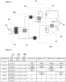
- FIG. 2 shows a schematic representation of a feed network for the antenna 10.
- the feed network has the function of dividing the input signal 20 and coupling it with suitable power levels and phases at four feed points P1... P4 into an antenna element 22, so that an antenna 10 with the desired polarization is created.
- the antenna element 22 is preferably an antenna patch, so that a patch antenna is created.
- a horizontal-linear polarization, a vertical-linear polarization, a right-handed circular polarization and a left-handed circular polarization are possible, i.e. four polarizations.
- the presented embodiment of the feed network only allows one circular polarization and thus three polarizations.
- the feed network has a first switching element 24, in the example shown a four-way switch with two input-side connections (DP4T, Double Pole Quadruple Throw), with which the input signal 20 is distributed to four connections.
- An antenna termination 26 is provided on the second input-side connection.
- the first switching element 24 is followed by a second switching element 28, which has, for example, two single-pole changeover switches (SPOT, Single Pole Double Throw).
- SPOT Single Pole Double Throw
- Four connecting lines from the four output-side connections of the first switching element 24 to the second switching element 28 are connected in pairs to the input-side connections of the single-pole changeover switches.
- a 90° hybrid coupler 30 is connected in one connecting line of each pair (Branchline Hybrid, 90° 3dB Divider).
- Two 180° power dividers 32 are connected to the output of the second switching element 28, in this embodiment as a ring coupler (ratrace hybrid, 180° 3dB divider), each of which has its own termination 34.
- each of the two partial signals is split again by the two single-pole changeover switches of the second switching element 28, and the resulting partial signals are fed to the feed points P1, P3 and P2, P4 with a 180° phase offset.
- FIG 3 shows an alternative representation of the feed network according to Figure 2 .
- the feed points P1...P4 are also arranged symmetrically, preferably in the form of a centered square.
- a phase offset of 90° for circular polarization or 180° for linear polarization is required, as provided by the feed network.
- a different, non-symmetrical arrangement is possible, but then requires a corresponding adjustment of the phases or only achieves the desired polarization approximately.
- Figure 4 shows a table with polarizations and associated switch positions of the feed network. The different polarizations are entered in the first column.
- the variants "Open 1" and “Open 2" are special cases that are not required for the actual operation of the antenna 10.
- the explicit wiring of the input signal 20 to an open or shorted to ground line end can be used, for example, for a reference measurement or calibration in order to measure the distance between the RFID front end with the transceiver 14 and the feed network. characterize, for example, to determine the line attenuation for remote antennas with longer cables.
- the second column shows how, for a respective polarization state of the first column, the input-side connections P1, P2 of the first switching element 24 are connected to its output-side connections P3... P6.
- the third and fourth columns show the switching state of the two single-pole changeover switches 28a-b of the second switching element 28. It should be noted that the designations Px are used several times for connections of different switching elements and also the feed points, but it is clear from the respective context what the designation refers to.
- the last four columns list the signals arriving at the feed points P1... P4, whereby the feed points in the table are as already in Figure 3 are designated out1... out4. Pin represents the respective input power.
- the first circular polarization according to the first line of the table is achieved in that the first switching element 24 establishes a connection to the inner connecting lines with the 90° hybrid coupler via P4 and P5, while the second switching element 28 passes these inner connecting lines via P3 of the first single-pole changeover switch 28a and P2 of the second single-pole changeover switch 28b to the 180° power dividers 32.
- the two partial signals output from the second switching element 28 are thus phase-shifted by 90° to one another, and the 180° power dividers thereby generate a 0° partial signal for the feed point P1, a 90° partial signal for P2, a 180° partial signal for P3 and a 270° partial signal for P4.
- the antenna 10 With its four feed points, the antenna 10 enables circular polarization with a low axial ratio. This makes the antenna 10 more robust against external interference, in particular metallic objects or reflectors near the antenna 10.
- partial signals with a phase offset of 180° can be coupled into two feed points. The attenuation is low for all polarizations. With linear polarization, the 90° hybrid coupler 30 is bypassed, so that the attenuation can remain even lower than with circular polarization.
- Figure 5 shows an exemplary concrete layout of the feed network on a circuit board or printed circuit board 38, which in Figure 3 is shown schematically.
- the antenna element 22 can be seen on the back of the circuit board 38.
- the structures of the 90° hybrid coupler 30 as well as those of the two 180° power dividers 32 use a conductor structure on a hexagonal grid according to the aforementioned DE 20 2015 105 455 U1 They are connected by means of connections implemented as impedance-matched microstrip lines 40.
- connecting lines 42 lead to the feed points P1 to P4, the symmetrical arrangement of which is shown in the associated schematic representation of the Figure 3 is even more recognizable.
- the special feature of the feed network shown is that it can be implemented in a single copper layer.
- the feed network does not require any crossings of the lines and therefore no change of the board layer and components required for line crossings, especially since corresponding crossings (vias) for impedance matching would require special attention in terms of attenuation and phase shift.
- a particularly compact design of the antenna 10 is created when the feed network is arranged on one side or surface of the circuit board 38 (bottom side), in particular in a single layer, and the antenna element 22 on the other side or surface (top side), in particular in the form of an antenna patch.
- Such an easily integrated structure also easily enables modular variant formation for different housings, as is the case in the as yet unpublished European patent application with the file number 22188151.9 described.
- Figure 6 shows a schematic representation of another embodiment of the supply network.
- the first switching element here is designed as a series arrangement of a two-pole changeover switch 24a (DPDT, Double Pole Double Throw) with two single-pole changeover switches 24b (SPOT, Single Port Double Throw).
- DPDT Double Pole Double Throw
- SPOT Single Port Double Throw
- FIG. 7 shows a schematic representation of another embodiment of the feed network.
- the first switching element provides additional connections 44 for a further antenna (not shown) in various switchable polarizations.
- two four-way switches SP4T
- DPDT two-pole changeover switch
- FIG 8 shows a schematic representation of another embodiment of the feed network.
- the 180° power dividers 32 are no longer designed as hybrid ring couplers, but as Wilkinson dividers 32a.
- the 180° phase offset is achieved by means of delay lines with a suitable delay.
- a Schiffmann phase shifter would be conceivable in order to enable power division with a suitable phase offset over a larger frequency range of the feed network.
- a 3dB 180° power division is also possible on the basis of the Wilkinson dividers 32a.
- the advantage over ring couplers is lower transmission loss when dimensioned correctly.
- the isolation between the output ports is lower, but this plays a minor role in the structure of the antenna 10, since the signals are to be coupled to the same antenna element 22 and there is a relatively good coupling between two opposite feed points, especially when designed as an antenna patch.
- Figure 9 shows another alternative to Figure 8 , in which the Wilkinson dividers 32a are now replaced by T-power dividers 32b. Otherwise, refer to the explanations for Figure 8
- the selection of suitable 180° power dividers 32, 32a, 32b is possible in all embodiments, this is not limited to the special representations of the Figures 8 and 9 limited.
- Figure 10 shows a schematic representation of another embodiment in which the feed network only supports one circular polarization and not both circular polarizations of both directions of rotation.
- the first switching element 24 used here is a three-way switch (SP3T, Single Pole Triple Throw). Only one connection to the 90° hybrid coupler 30 can be switched, the other connection is permanently connected to an antenna adapter 48. The direction of rotation of the circular polarization can only be selected by circuit design.
- the feed network according to Figure 10 allowed This means that there is only a choice between three polarizations and it has the advantage of generating lower losses due to the reduced number of switches and the simpler design of the switch components.
Landscapes
- Engineering & Computer Science (AREA)
- Physics & Mathematics (AREA)
- Health & Medical Sciences (AREA)
- Computer Networks & Wireless Communication (AREA)
- Toxicology (AREA)
- General Physics & Mathematics (AREA)
- Theoretical Computer Science (AREA)
- Microelectronics & Electronic Packaging (AREA)
- Computer Hardware Design (AREA)
- Electromagnetism (AREA)
- General Health & Medical Sciences (AREA)
- Artificial Intelligence (AREA)
- Computer Vision & Pattern Recognition (AREA)
- Variable-Direction Aerials And Aerial Arrays (AREA)
- Waveguide Aerials (AREA)
Priority Applications (5)
| Application Number | Priority Date | Filing Date | Title |
|---|---|---|---|
| EP23171296.9A EP4459789B1 (fr) | 2023-05-03 | 2023-05-03 | Antenne pour dispositif de lecture rfid à commutation de polarisation |
| JP2024035362A JP7688188B2 (ja) | 2023-05-03 | 2024-03-07 | 偏波切り換え装置を有するrfid読み取り装置用アンテナ |
| CN202410360098.5A CN118899660A (zh) | 2023-05-03 | 2024-03-27 | 用于rfid阅读器的极化切换的天线 |
| KR1020240047214A KR20240161023A (ko) | 2023-05-03 | 2024-04-08 | 편파 스위칭을 하는 rfid 리딩 디바이스의 안테나 |
| US18/653,654 US20240372244A1 (en) | 2023-05-03 | 2024-05-02 | Antenna for an rfid reading device with polarization switching |
Applications Claiming Priority (1)
| Application Number | Priority Date | Filing Date | Title |
|---|---|---|---|
| EP23171296.9A EP4459789B1 (fr) | 2023-05-03 | 2023-05-03 | Antenne pour dispositif de lecture rfid à commutation de polarisation |
Publications (2)
| Publication Number | Publication Date |
|---|---|
| EP4459789A1 true EP4459789A1 (fr) | 2024-11-06 |
| EP4459789B1 EP4459789B1 (fr) | 2025-04-02 |
Family
ID=86329016
Family Applications (1)
| Application Number | Title | Priority Date | Filing Date |
|---|---|---|---|
| EP23171296.9A Active EP4459789B1 (fr) | 2023-05-03 | 2023-05-03 | Antenne pour dispositif de lecture rfid à commutation de polarisation |
Country Status (5)
| Country | Link |
|---|---|
| US (1) | US20240372244A1 (fr) |
| EP (1) | EP4459789B1 (fr) |
| JP (1) | JP7688188B2 (fr) |
| KR (1) | KR20240161023A (fr) |
| CN (1) | CN118899660A (fr) |
Citations (11)
| Publication number | Priority date | Publication date | Assignee | Title |
|---|---|---|---|---|
| US7068224B2 (en) | 2004-03-12 | 2006-06-27 | Alien Technology Corporation | Switching patch antenna |
| KR100902496B1 (ko) * | 2007-08-31 | 2009-06-15 | 주식회사 이엠따블유안테나 | 편파변환 안테나 및 통신 장치 |
| KR100976087B1 (ko) | 2008-07-11 | 2010-08-16 | 주식회사 이엠따블유 | 4중 편파 안테나 모듈 및 이를 포함하는 무선 송수신 장치 |
| US20110032079A1 (en) | 2009-08-10 | 2011-02-10 | Rf Controls, Llc | Antenna switching arrangement |
| US7932867B2 (en) | 2007-04-26 | 2011-04-26 | Round Rock Research, Llc | Methods and systems of changing antenna polarization |
| EP2368210B1 (fr) | 2008-12-18 | 2012-12-26 | Kathrein-Werke KG | Procédé de commande d une antenne rfid et système d antenne rfid associé |
| DE202015106025U1 (de) | 2015-11-10 | 2015-11-26 | Sick Ag | RFID-Antennenanordnung |
| DE202015105455U1 (de) | 2014-11-19 | 2016-02-22 | Sick Ag | Leitungsstruktur für ein Hochfrequenzsignal |
| EP3220554A1 (fr) | 2016-03-14 | 2017-09-20 | Denso Wave Incorporated | Appareil d'antenne pour communiquer avec un support de communication sans contact par l'intermédiaire d'ondes électromagnétiques |
| EP1987468B1 (fr) | 2006-02-15 | 2018-05-23 | Tyco Fire & Security GmbH | Multiplexeur rfid commuté par rf |
| KR101868464B1 (ko) * | 2017-04-20 | 2018-06-18 | 경상대학교산학협력단 | 편파 조절 안테나 장치 및 이를 구비한 무선 통신 장치 |
Family Cites Families (14)
| Publication number | Priority date | Publication date | Assignee | Title |
|---|---|---|---|---|
| JPH07162227A (ja) * | 1993-12-07 | 1995-06-23 | Matsushita Electric Ind Co Ltd | 偏波共用アンテナシステム |
| US6839036B1 (en) * | 2003-07-29 | 2005-01-04 | Bae Systems Information And Electronic Systems Integration, Inc. | Concatenated Vivaldi notch/meander line loaded antennas |
| US6882322B1 (en) * | 2003-10-14 | 2005-04-19 | Bae Systems Information And Electronic Systems Integration Inc. | Gapless concatenated Vivaldi notch/meander line loaded antennas |
| US8289209B2 (en) | 2009-04-13 | 2012-10-16 | Viasat, Inc. | Active butler and blass matrices |
| CN201435450Y (zh) * | 2009-06-30 | 2010-03-31 | 华南理工大学 | 极化可重构射频识别圆极化阅读器天线 |
| US9379438B1 (en) * | 2009-12-01 | 2016-06-28 | Viasat, Inc. | Fragmented aperture for the Ka/K/Ku frequency bands |
| EP2442255A1 (fr) * | 2010-09-27 | 2012-04-18 | Sick AG | Dispositif de lecture RFID |
| US9502746B2 (en) * | 2015-02-04 | 2016-11-22 | Tyco Electronics Corporation | 180 degree hybrid coupler and dual-linearly polarized antenna feed network |
| WO2022264973A1 (fr) * | 2021-06-18 | 2022-12-22 | Agc株式会社 | Dispositif antenne et verre à vitre pour bâtiment |
| US12469975B2 (en) * | 2022-11-30 | 2025-11-11 | Zebra Technologies Corporation | Patch antenna assembly with parasitic patch and capacitive loading elements |
| KR20240143135A (ko) * | 2023-03-23 | 2024-10-02 | 주식회사 에이치엘클레무브 | 레이더의 위상 오차 보상 장치 및 방법과, 그를 포함하는 레이더 장치 |
| KR20240148092A (ko) * | 2023-04-03 | 2024-10-11 | 주식회사 에이치엘클레무브 | 레이더 신호 처리 장치 및 방법과, 그를 포함하는 레이더 장치 |
| US12381328B2 (en) * | 2023-12-14 | 2025-08-05 | Auden Techno Corp. | Dual circularly polarized antenna array |
| TWI886769B (zh) * | 2024-01-24 | 2025-06-11 | 明泰科技股份有限公司 | 具水平極化全向性之多頻天線結構 |
-
2023
- 2023-05-03 EP EP23171296.9A patent/EP4459789B1/fr active Active
-
2024
- 2024-03-07 JP JP2024035362A patent/JP7688188B2/ja active Active
- 2024-03-27 CN CN202410360098.5A patent/CN118899660A/zh active Pending
- 2024-04-08 KR KR1020240047214A patent/KR20240161023A/ko active Pending
- 2024-05-02 US US18/653,654 patent/US20240372244A1/en active Pending
Patent Citations (11)
| Publication number | Priority date | Publication date | Assignee | Title |
|---|---|---|---|---|
| US7068224B2 (en) | 2004-03-12 | 2006-06-27 | Alien Technology Corporation | Switching patch antenna |
| EP1987468B1 (fr) | 2006-02-15 | 2018-05-23 | Tyco Fire & Security GmbH | Multiplexeur rfid commuté par rf |
| US7932867B2 (en) | 2007-04-26 | 2011-04-26 | Round Rock Research, Llc | Methods and systems of changing antenna polarization |
| KR100902496B1 (ko) * | 2007-08-31 | 2009-06-15 | 주식회사 이엠따블유안테나 | 편파변환 안테나 및 통신 장치 |
| KR100976087B1 (ko) | 2008-07-11 | 2010-08-16 | 주식회사 이엠따블유 | 4중 편파 안테나 모듈 및 이를 포함하는 무선 송수신 장치 |
| EP2368210B1 (fr) | 2008-12-18 | 2012-12-26 | Kathrein-Werke KG | Procédé de commande d une antenne rfid et système d antenne rfid associé |
| US20110032079A1 (en) | 2009-08-10 | 2011-02-10 | Rf Controls, Llc | Antenna switching arrangement |
| DE202015105455U1 (de) | 2014-11-19 | 2016-02-22 | Sick Ag | Leitungsstruktur für ein Hochfrequenzsignal |
| DE202015106025U1 (de) | 2015-11-10 | 2015-11-26 | Sick Ag | RFID-Antennenanordnung |
| EP3220554A1 (fr) | 2016-03-14 | 2017-09-20 | Denso Wave Incorporated | Appareil d'antenne pour communiquer avec un support de communication sans contact par l'intermédiaire d'ondes électromagnétiques |
| KR101868464B1 (ko) * | 2017-04-20 | 2018-06-18 | 경상대학교산학협력단 | 편파 조절 안테나 장치 및 이를 구비한 무선 통신 장치 |
Also Published As
| Publication number | Publication date |
|---|---|
| EP4459789B1 (fr) | 2025-04-02 |
| JP2024160935A (ja) | 2024-11-15 |
| CN118899660A (zh) | 2024-11-05 |
| US20240372244A1 (en) | 2024-11-07 |
| JP7688188B2 (ja) | 2025-06-03 |
| KR20240161023A (ko) | 2024-11-12 |
Similar Documents
| Publication | Publication Date | Title |
|---|---|---|
| DE10237823A1 (de) | Kalibriereinrichtung für ein Antennen-Array sowie zugehöriges Antennen-Array und Verfahren zu dessem Betrieb | |
| EP2101279A2 (fr) | Circuit réglable et unité de lecteur RFID | |
| EP1530816B9 (fr) | Dispositif de calibrage pour un reseau d'antennes commutable et procede pour faire fonctionner ce dispositif | |
| DE102013003916A1 (de) | Radarvorrichtung | |
| WO2011082971A1 (fr) | Câble de liaison pour relier par câble électrique ou par fibres optiques deux appareils d'un système | |
| DE602005000802T2 (de) | Breitbandige Rundum-Antennensystem | |
| EP2368210B1 (fr) | Procédé de commande d une antenne rfid et système d antenne rfid associé | |
| EP3861590B1 (fr) | Système de communication | |
| EP4459789B1 (fr) | Antenne pour dispositif de lecture rfid à commutation de polarisation | |
| DE1766185A1 (de) | Antennensysteme | |
| EP0588179B1 (fr) | Dispositif pour mettre en service un réseau d'antennes à commande de phase à large bande | |
| CH676903A5 (en) | Information transmission system for train - uses coded microwave signals fed between successive train sections | |
| DE102016014589B4 (de) | Antennenanordnung | |
| DE2118550A1 (de) | Elektronisch abtastendes Antennensystem | |
| EP4542765B1 (fr) | Dispositif d'antenne pour la réception et l'émission d'ondes électromagnétiques de polarisations différentes | |
| DE60218901T2 (de) | Verfahren und system zur übertragung von trägersignalen zwischen einem ersten und einem zweiten antennennetzwerk | |
| DE102019100128A1 (de) | Vorichtung und verfahren zum senden eines hf-signals | |
| EP0227005B1 (fr) | Dispositif d'émission à deux émetteurs haute fréquence émettant des fréquences différentes avec des diagrammes de rayonnement différents | |
| DE2625062A1 (de) | Phasenschieber zur verwendung bei einer elektronisch phasengesteuerten antenne | |
| DE3545639C1 (en) | Transmitter operating at at least two frequencies - uses single VHF antenna array with different polar diagrams | |
| DE202016008105U1 (de) | Kontaktloser Steckverbinder | |
| EP3443682A1 (fr) | Connecteur sans contact | |
| DE102017112441B4 (de) | Beamforming-Struktur, Antennenanordnung mit einer Beamforming-Struktur sowie Sende- und/oder Empfangsvorrichtung mit einer Beamforming-Struktur | |
| DE19532470B4 (de) | Selektiver Multikoppler | |
| DE1952053C3 (de) | Mikrowellenantenne mit mehreren parallelen strahlenden Leitungen |
Legal Events
| Date | Code | Title | Description |
|---|---|---|---|
| STAA | Information on the status of an ep patent application or granted ep patent |
Free format text: STATUS: EXAMINATION IS IN PROGRESS |
|
| PUAI | Public reference made under article 153(3) epc to a published international application that has entered the european phase |
Free format text: ORIGINAL CODE: 0009012 |
|
| 17P | Request for examination filed |
Effective date: 20240111 |
|
| AK | Designated contracting states |
Kind code of ref document: A1 Designated state(s): AL AT BE BG CH CY CZ DE DK EE ES FI FR GB GR HR HU IE IS IT LI LT LU LV MC ME MK MT NL NO PL PT RO RS SE SI SK SM TR |
|
| GRAP | Despatch of communication of intention to grant a patent |
Free format text: ORIGINAL CODE: EPIDOSNIGR1 |
|
| STAA | Information on the status of an ep patent application or granted ep patent |
Free format text: STATUS: GRANT OF PATENT IS INTENDED |
|
| INTG | Intention to grant announced |
Effective date: 20241129 |
|
| GRAS | Grant fee paid |
Free format text: ORIGINAL CODE: EPIDOSNIGR3 |
|
| GRAA | (expected) grant |
Free format text: ORIGINAL CODE: 0009210 |
|
| STAA | Information on the status of an ep patent application or granted ep patent |
Free format text: STATUS: THE PATENT HAS BEEN GRANTED |
|
| AK | Designated contracting states |
Kind code of ref document: B1 Designated state(s): AL AT BE BG CH CY CZ DE DK EE ES FI FR GB GR HR HU IE IS IT LI LT LU LV MC ME MK MT NL NO PL PT RO RS SE SI SK SM TR |
|
| REG | Reference to a national code |
Ref country code: GB Ref legal event code: FG4D Free format text: NOT ENGLISH |
|
| REG | Reference to a national code |
Ref country code: CH Ref legal event code: EP |
|
| REG | Reference to a national code |
Ref country code: DE Ref legal event code: R096 Ref document number: 502023000753 Country of ref document: DE |
|
| REG | Reference to a national code |
Ref country code: IE Ref legal event code: FG4D Free format text: LANGUAGE OF EP DOCUMENT: GERMAN |
|
| PGFP | Annual fee paid to national office [announced via postgrant information from national office to epo] |
Ref country code: DE Payment date: 20250528 Year of fee payment: 3 |
|
| PGFP | Annual fee paid to national office [announced via postgrant information from national office to epo] |
Ref country code: LU Payment date: 20250528 Year of fee payment: 3 Ref country code: BE Payment date: 20250528 Year of fee payment: 3 |
|
| PGFP | Annual fee paid to national office [announced via postgrant information from national office to epo] |
Ref country code: FR Payment date: 20250528 Year of fee payment: 3 |
|
| PGFP | Annual fee paid to national office [announced via postgrant information from national office to epo] |
Ref country code: AT Payment date: 20250721 Year of fee payment: 3 |
|
| REG | Reference to a national code |
Ref country code: NL Ref legal event code: MP Effective date: 20250402 |
|
| PG25 | Lapsed in a contracting state [announced via postgrant information from national office to epo] |
Ref country code: NL Free format text: LAPSE BECAUSE OF FAILURE TO SUBMIT A TRANSLATION OF THE DESCRIPTION OR TO PAY THE FEE WITHIN THE PRESCRIBED TIME-LIMIT Effective date: 20250402 |
|
| PG25 | Lapsed in a contracting state [announced via postgrant information from national office to epo] |
Ref country code: FI Free format text: LAPSE BECAUSE OF FAILURE TO SUBMIT A TRANSLATION OF THE DESCRIPTION OR TO PAY THE FEE WITHIN THE PRESCRIBED TIME-LIMIT Effective date: 20250402 Ref country code: ES Free format text: LAPSE BECAUSE OF FAILURE TO SUBMIT A TRANSLATION OF THE DESCRIPTION OR TO PAY THE FEE WITHIN THE PRESCRIBED TIME-LIMIT Effective date: 20250402 Ref country code: PT Free format text: LAPSE BECAUSE OF FAILURE TO SUBMIT A TRANSLATION OF THE DESCRIPTION OR TO PAY THE FEE WITHIN THE PRESCRIBED TIME-LIMIT Effective date: 20250804 |
|
| REG | Reference to a national code |
Ref country code: LT Ref legal event code: MG9D |
|
| PG25 | Lapsed in a contracting state [announced via postgrant information from national office to epo] |
Ref country code: GR Free format text: LAPSE BECAUSE OF FAILURE TO SUBMIT A TRANSLATION OF THE DESCRIPTION OR TO PAY THE FEE WITHIN THE PRESCRIBED TIME-LIMIT Effective date: 20250703 Ref country code: NO Free format text: LAPSE BECAUSE OF FAILURE TO SUBMIT A TRANSLATION OF THE DESCRIPTION OR TO PAY THE FEE WITHIN THE PRESCRIBED TIME-LIMIT Effective date: 20250702 |
|
| PG25 | Lapsed in a contracting state [announced via postgrant information from national office to epo] |
Ref country code: PL Free format text: LAPSE BECAUSE OF FAILURE TO SUBMIT A TRANSLATION OF THE DESCRIPTION OR TO PAY THE FEE WITHIN THE PRESCRIBED TIME-LIMIT Effective date: 20250402 |
|
| PG25 | Lapsed in a contracting state [announced via postgrant information from national office to epo] |
Ref country code: BG Free format text: LAPSE BECAUSE OF FAILURE TO SUBMIT A TRANSLATION OF THE DESCRIPTION OR TO PAY THE FEE WITHIN THE PRESCRIBED TIME-LIMIT Effective date: 20250402 |
|
| PG25 | Lapsed in a contracting state [announced via postgrant information from national office to epo] |
Ref country code: HR Free format text: LAPSE BECAUSE OF FAILURE TO SUBMIT A TRANSLATION OF THE DESCRIPTION OR TO PAY THE FEE WITHIN THE PRESCRIBED TIME-LIMIT Effective date: 20250402 |
|
| PG25 | Lapsed in a contracting state [announced via postgrant information from national office to epo] |
Ref country code: RS Free format text: LAPSE BECAUSE OF FAILURE TO SUBMIT A TRANSLATION OF THE DESCRIPTION OR TO PAY THE FEE WITHIN THE PRESCRIBED TIME-LIMIT Effective date: 20250702 |
|
| PG25 | Lapsed in a contracting state [announced via postgrant information from national office to epo] |
Ref country code: IS Free format text: LAPSE BECAUSE OF FAILURE TO SUBMIT A TRANSLATION OF THE DESCRIPTION OR TO PAY THE FEE WITHIN THE PRESCRIBED TIME-LIMIT Effective date: 20250802 |
|
| PG25 | Lapsed in a contracting state [announced via postgrant information from national office to epo] |
Ref country code: LV Free format text: LAPSE BECAUSE OF FAILURE TO SUBMIT A TRANSLATION OF THE DESCRIPTION OR TO PAY THE FEE WITHIN THE PRESCRIBED TIME-LIMIT Effective date: 20250402 |
|
| REG | Reference to a national code |
Ref country code: DE Ref legal event code: R097 Ref document number: 502023000753 Country of ref document: DE |
|
| PG25 | Lapsed in a contracting state [announced via postgrant information from national office to epo] |
Ref country code: SM Free format text: LAPSE BECAUSE OF FAILURE TO SUBMIT A TRANSLATION OF THE DESCRIPTION OR TO PAY THE FEE WITHIN THE PRESCRIBED TIME-LIMIT Effective date: 20250402 Ref country code: DK Free format text: LAPSE BECAUSE OF FAILURE TO SUBMIT A TRANSLATION OF THE DESCRIPTION OR TO PAY THE FEE WITHIN THE PRESCRIBED TIME-LIMIT Effective date: 20250402 |
|
| PG25 | Lapsed in a contracting state [announced via postgrant information from national office to epo] |
Ref country code: CZ Free format text: LAPSE BECAUSE OF FAILURE TO SUBMIT A TRANSLATION OF THE DESCRIPTION OR TO PAY THE FEE WITHIN THE PRESCRIBED TIME-LIMIT Effective date: 20250402 |
|
| PG25 | Lapsed in a contracting state [announced via postgrant information from national office to epo] |
Ref country code: EE Free format text: LAPSE BECAUSE OF FAILURE TO SUBMIT A TRANSLATION OF THE DESCRIPTION OR TO PAY THE FEE WITHIN THE PRESCRIBED TIME-LIMIT Effective date: 20250402 |
|
| PG25 | Lapsed in a contracting state [announced via postgrant information from national office to epo] |
Ref country code: SK Free format text: LAPSE BECAUSE OF FAILURE TO SUBMIT A TRANSLATION OF THE DESCRIPTION OR TO PAY THE FEE WITHIN THE PRESCRIBED TIME-LIMIT Effective date: 20250402 |
|
| PG25 | Lapsed in a contracting state [announced via postgrant information from national office to epo] |
Ref country code: IT Free format text: LAPSE BECAUSE OF FAILURE TO SUBMIT A TRANSLATION OF THE DESCRIPTION OR TO PAY THE FEE WITHIN THE PRESCRIBED TIME-LIMIT Effective date: 20250402 |
|
| PG25 | Lapsed in a contracting state [announced via postgrant information from national office to epo] |
Ref country code: MC Free format text: LAPSE BECAUSE OF FAILURE TO SUBMIT A TRANSLATION OF THE DESCRIPTION OR TO PAY THE FEE WITHIN THE PRESCRIBED TIME-LIMIT Effective date: 20250402 |
|
| PLBE | No opposition filed within time limit |
Free format text: ORIGINAL CODE: 0009261 |
|
| STAA | Information on the status of an ep patent application or granted ep patent |
Free format text: STATUS: NO OPPOSITION FILED WITHIN TIME LIMIT |
|
| REG | Reference to a national code |
Ref country code: CH Ref legal event code: L10 Free format text: ST27 STATUS EVENT CODE: U-0-0-L10-L00 (AS PROVIDED BY THE NATIONAL OFFICE) Effective date: 20260211 |
|
| 26N | No opposition filed |
Effective date: 20260105 |
|
| PG25 | Lapsed in a contracting state [announced via postgrant information from national office to epo] |
Ref country code: RO Free format text: LAPSE BECAUSE OF FAILURE TO SUBMIT A TRANSLATION OF THE DESCRIPTION OR TO PAY THE FEE WITHIN THE PRESCRIBED TIME-LIMIT Effective date: 20250402 |
|
| PG25 | Lapsed in a contracting state [announced via postgrant information from national office to epo] |
Ref country code: IE Free format text: LAPSE BECAUSE OF NON-PAYMENT OF DUE FEES Effective date: 20250503 |