EP4465146A1 - Referenzspannungserzeugungsschaltung - Google Patents
Referenzspannungserzeugungsschaltung Download PDFInfo
- Publication number
- EP4465146A1 EP4465146A1 EP24174416.8A EP24174416A EP4465146A1 EP 4465146 A1 EP4465146 A1 EP 4465146A1 EP 24174416 A EP24174416 A EP 24174416A EP 4465146 A1 EP4465146 A1 EP 4465146A1
- Authority
- EP
- European Patent Office
- Prior art keywords
- transistor
- voltage
- node
- bridge
- supply
- Prior art date
- Legal status (The legal status is an assumption and is not a legal conclusion. Google has not performed a legal analysis and makes no representation as to the accuracy of the status listed.)
- Pending
Links
- 230000000875 corresponding effect Effects 0.000 description 12
- 238000002955 isolation Methods 0.000 description 3
- 230000008878 coupling Effects 0.000 description 2
- 238000010168 coupling process Methods 0.000 description 2
- 238000005859 coupling reaction Methods 0.000 description 2
- 235000021183 entrée Nutrition 0.000 description 2
- 239000004020 conductor Substances 0.000 description 1
- 230000002596 correlated effect Effects 0.000 description 1
- 230000014509 gene expression Effects 0.000 description 1
- 238000004519 manufacturing process Methods 0.000 description 1
- 239000000463 material Substances 0.000 description 1
- 229910044991 metal oxide Inorganic materials 0.000 description 1
- 150000004706 metal oxides Chemical class 0.000 description 1
- 238000000034 method Methods 0.000 description 1
- 239000004065 semiconductor Substances 0.000 description 1
Images

Classifications
-
- G—PHYSICS
- G05—CONTROLLING; REGULATING
- G05F—SYSTEMS FOR REGULATING ELECTRIC OR MAGNETIC VARIABLES
- G05F3/00—Non-retroactive systems for regulating electric variables by using an uncontrolled element, or an uncontrolled combination of elements, such element or such combination having self-regulating properties
- G05F3/02—Regulating voltage or current
- G05F3/08—Regulating voltage or current wherein the variable is DC
- G05F3/10—Regulating voltage or current wherein the variable is DC using uncontrolled devices with non-linear characteristics
- G05F3/16—Regulating voltage or current wherein the variable is DC using uncontrolled devices with non-linear characteristics being semiconductor devices
-
- G—PHYSICS
- G05—CONTROLLING; REGULATING
- G05F—SYSTEMS FOR REGULATING ELECTRIC OR MAGNETIC VARIABLES
- G05F1/00—Automatic systems in which deviations of an electric quantity from one or more predetermined values are detected at the output of the system and fed back to a device within the system to restore the detected quantity to its predetermined value or values, i.e. retroactive systems
- G05F1/10—Regulating voltage or current
- G05F1/46—Regulating voltage or current wherein the variable actually regulated by the final control device is DC
- G05F1/468—Regulating voltage or current wherein the variable actually regulated by the final control device is DC characterised by reference voltage circuitry, e.g. soft start, remote shutdown
-
- G—PHYSICS
- G05—CONTROLLING; REGULATING
- G05F—SYSTEMS FOR REGULATING ELECTRIC OR MAGNETIC VARIABLES
- G05F3/00—Non-retroactive systems for regulating electric variables by using an uncontrolled element, or an uncontrolled combination of elements, such element or such combination having self-regulating properties
- G05F3/02—Regulating voltage or current
- G05F3/08—Regulating voltage or current wherein the variable is DC
- G05F3/10—Regulating voltage or current wherein the variable is DC using uncontrolled devices with non-linear characteristics
- G05F3/16—Regulating voltage or current wherein the variable is DC using uncontrolled devices with non-linear characteristics being semiconductor devices
- G05F3/20—Regulating voltage or current wherein the variable is DC using uncontrolled devices with non-linear characteristics being semiconductor devices using diode- transistor combinations
- G05F3/26—Current mirrors
- G05F3/262—Current mirrors using field-effect transistors only
-
- H—ELECTRICITY
- H03—ELECTRONIC CIRCUITRY
- H03F—AMPLIFIERS
- H03F1/00—Details of amplifiers with only discharge tubes, only semiconductor devices or only unspecified devices as amplifying elements
- H03F1/02—Modifications of amplifiers to raise the efficiency, e.g. gliding Class A stages, use of an auxiliary oscillation
- H03F1/0205—Modifications of amplifiers to raise the efficiency, e.g. gliding Class A stages, use of an auxiliary oscillation in transistor amplifiers
- H03F1/0261—Modifications of amplifiers to raise the efficiency, e.g. gliding Class A stages, use of an auxiliary oscillation in transistor amplifiers with control of the polarisation voltage or current, e.g. gliding Class A
-
- H—ELECTRICITY
- H03—ELECTRONIC CIRCUITRY
- H03F—AMPLIFIERS
- H03F1/00—Details of amplifiers with only discharge tubes, only semiconductor devices or only unspecified devices as amplifying elements
- H03F1/08—Modifications of amplifiers to reduce detrimental influences of internal impedances of amplifying elements
- H03F1/22—Modifications of amplifiers to reduce detrimental influences of internal impedances of amplifying elements by use of cascode coupling, i.e. earthed cathode or emitter stage followed by earthed grid or base stage respectively
- H03F1/223—Modifications of amplifiers to reduce detrimental influences of internal impedances of amplifying elements by use of cascode coupling, i.e. earthed cathode or emitter stage followed by earthed grid or base stage respectively with MOSFET's
-
- H—ELECTRICITY
- H03—ELECTRONIC CIRCUITRY
- H03F—AMPLIFIERS
- H03F3/00—Amplifiers with only discharge tubes or only semiconductor devices as amplifying elements
- H03F3/45—Differential amplifiers
- H03F3/45071—Differential amplifiers with semiconductor devices only
- H03F3/45076—Differential amplifiers with semiconductor devices only characterised by the way of implementation of the active amplifying circuit in the differential amplifier
- H03F3/45179—Differential amplifiers with semiconductor devices only characterised by the way of implementation of the active amplifying circuit in the differential amplifier using MOSFET transistors as the active amplifying circuit
- H03F3/45183—Long tailed pairs
Definitions
- This description relates generally to integrated electronic circuits, and, more particularly, to a reference voltage generation device.
- Integrated circuits are known in which a first supply voltage is provided, for example available on a connection pad of a chip comprising these integrated circuits, and a second supply voltage, for example generated internally of the chip, having a nominal value lower than that of the first voltage.
- some comprise at least one device, such as for example a resistive memory, which is supplied by the first supply voltage to be functional.
- this device is implemented with MOS (Metal Oxide Semiconductor) transistors having a voltage withstand limit value lower than the nominal value of the first voltage.
- MOS Metal Oxide Semiconductor
- cascode architectures or stacked architectures are used.
- two transistors are in series with each other and one of the two transistors receives a bias or reference voltage on its gate.
- the second voltage must be applied to the cascode structures before the first voltage so as not to destroy the transistors. Furthermore, when the variations of the first and second voltages are not correlated, this degrades the performance of the cascode structures, and therefore of the device.
- the generated voltage can only take one value which is determined by the circuit used to generate this voltage.
- the generated voltage can then be too low to be used as a reference voltage for cascode structures. This is the case, for example, when the difference between the generated voltage and the first supply voltage is greater than the voltage rating of the transistors of the cascode structures.
- the generated voltage can be too high to be used as a reference voltage for cascode structures. This is the case, for example, when cascode structures must operate when the first voltage is at its nominal value, but also when the first voltage is at a lower value. corresponding, for example, to a low-consumption operating mode.
- One embodiment provides a circuit overcoming all or part of the drawbacks of known solutions for generating a reference voltage.
- One embodiment provides a system comprising a device as described above, and a circuit configured to receive said command, the first voltage and the second voltage, and to provide said binary signal.
- the expressions “approximately”, “approximately”, “substantially”, and “of the order of” mean to within 10%, preferably to within 5%.
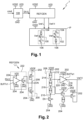
- FIG. 1 represents, schematically and in the form of blocks, an example of an electronic system 1 comprising a REFGEN device for generating a reference voltage according to one embodiment.
- the system corresponding for example to a portion of an integrated circuit chip, comprises an IP device, for example a resistive memory, and the REFGEN device.
- IP device for example a resistive memory
- REFGEN device for example a resistive memory
- the IP device is powered by a VDDE supply voltage, for example available on a connection pad of the chip.
- the VDDE voltage has a nominal value substantially equal to 3.3 V.
- the IP device comprises a terminal configured to receive the voltage VDDE, and another terminal configured to receive a reference potential GND, for example ground, to which the voltage VDDE is referenced.
- the IP device includes MOS transistor cascode structures.
- the IP device includes N-channel MOS transistor cascode structures 100 and P-channel MOS transistor cascode structures 102.
- each structure 100 comprises two N-channel MOS transistors T1 and T2 connected in series between a node 104 receiving the voltage VDDE and a node 106 receiving the potential GND.
- the transistor T1 has its source connected to the node 106 and its drain connected to the source of the transistor T2, the source of the transistor T2 being coupled to the node 104 by a load L.
- the gate of the transistor T2 is configured to receive a reference or bias voltage VrefH.
- the transistor T2 is, for example, called a cascode transistor.
- the gate of the transistor T1 is configured to receive a control voltage between 0 V and the bias voltage VrefH.
- each structure 102 comprises two P-channel MOS transistors T3 and T4 connected in series between nodes 104 and 106.
- Transistor T2 has its source connected to node 104 and its drain connected to the source of transistor T2, the source of transistor T2 being coupled to node 106 by a load L.
- the gate of transistor T4 is configured to receive a reference or bias voltage VrefL.
- Transistor T4 is, for example, called a cascode transistor.
- the gate of transistor T3 is configured to receive a control voltage between the reference voltage VrefL and the supply voltage VDDE.
- Vmax is the maximum voltage that can be applied between the gate and the source or between the source and the drain of each of the transistors of the IP device without damaging the transistor.
- Vmax is the voltage withstand limit of the MOS transistors of the IP device.
- the voltages VrefL and VrefH have different values.
- the voltage VrefL is chosen to be equal to the voltage VDEE minus the voltage VrefH.
- the voltages VrefL and VrefH have the same value.
- VrefH and VrefL voltages are received by the IP device.
- the REFGEN device is configured to provide the voltages VrefL and VrefH.
- the REFGEN device is powered by the voltage VDDE.
- the REFGEN device has, for example, one terminal receiving the voltage VDDE, and another terminal receiving the reference potential GND.
- the REFGEN device is further configured to receive a supply voltage VDD and a binary signal EN-S.
- the voltage VDD has a lower nominal value than that of the voltage VDDE.
- the voltage VDD is lower than the voltage withstand limit Vmax.
- the result of subtracting the nominal value of the voltage VDD from that of the voltage VDDE is lower than the voltage withstand limit of the transistors T1, T2, T3 and T4 of the IP device.
- the voltage VDD is a voltage generated by a circuit (not shown) of the integrated circuit chip comprising the system 1.
- the EN-S signal is a binary signal whose low level corresponds to a zero voltage, and whose high level corresponds to the VDD voltage.
- the EN-S signal is configured to be at its low level by default.
- the EN-S signal is further configured to be at its low level when the current value of the VDDE voltage is greater than the Vmax voltage.
- the level of the EN-S signal is determined by a cmd control signal. For example, setting the EN-S signal with the cmd signal when the VDDE voltage is less than the Vmax voltage corresponds to a low-power operating mode where the VDDE voltage is at a current value lower than its nominal value, for example a current value equal to the nominal value of the VDD voltage.
- the system 1 comprises a circuit 108 configured to receive the voltages VDDE and VDD, the potential GND and the signal cmd, and to provide the signal EN-S.
- a circuit 108 configured to receive the voltages VDDE and VDD, the potential GND and the signal cmd, and to provide the signal EN-S.
- the implementation of such a circuit 108, and, more generally, the generation of the signal EN-S, are within the capabilities of the person skilled in the art, for example by using standard power-on reset (PoR) circuits.
- PoR power-on reset
- the REFGEN circuit does not receive the EN-S signal and the VDD voltage.
- the IP device comprises structures 100 and 102, and the REFGEN device therefore provides both voltages VrefH and VrefL.
- the IP device does not comprise structure 100 and the REFGEN device then provides only voltage VrefL, or, conversely, the IP device does not comprise structure 102 and the REFGEN device then provides only voltage VrefH.
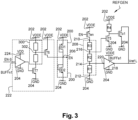
- FIG 2 illustrates, in the form of a circuit, an embodiment of the REFGEN circuit of the figure 1 .
- the REFGEN device is configured to provide only the VrefH voltage.
- the REFGEN device includes a voltage divider bridge 200.
- the bridge 200 is connected between a node 202 configured to receive the VDDE voltage, and a node 204 configured to receive the GND potential.
- the bridge 200 has one end connected to the node 202 and one end connected to the node 204.
- the bridge 200 comprises one or more P-channel MOS transistors connected in series between the node 202 and an intermediate node 206 of the bridge 200. Each of these P-channel transistors is connected as a diode, or, in other words, has its drain connected to its gate. Each of these P-channel transistors has its source on the side of the node 202. figure 2 , these P-channel transistors are represented as a single P-channel MOS transistor, D1.
- the bridge 200 comprises one or more N-channel MOS transistors connected in series between the node 206 and the node 204. Each of these N-channel transistors is connected as a diode, or, in other words, has its drain connected to its gate. Each of these N-channel transistors has its source on the side of the node 204. figure 2 , these N-channel transistors are represented as a single N-channel MOS transistor, D2.
- the P-channel MOS transistors of the bridge 200 are replaced by diodes, for example diodes having their anodes on the side of the node 202, and the N-channel MOS transistors of the bridge 200 are also replaced by diodes, for example diodes having their anodes on the side of the node 206.
- the P-channel transistors of the bridge 200 are replaced by a resistive element comprising one or more resistors in series between the nodes 202 and 206, and the N-channel transistors of the bridge 200 are replaced by another resistive element comprising one or more resistors in series between the nodes 206 and 204.
- the REFGEN device comprises a MOS transistor Ten and a resistive voltage divider bridge 208, the transistor Ten and the bridge 208 being connected in series between the nodes 202 and 204.
- Transistor Ten has its gate connected to node 206 on which a voltage EN is available.
- the source of transistor Ten is connected to node 204 in the embodiment of the figure 2 .
- transistor Ten is N-channel.
- the divider bridge 208 has one end 210 connected to the drain of the transistor Ten.
- the divider bridge 208 has another end 212 connected to the node 202 in the embodiment of the figure 2 .
- the bridge 208 comprises, for example, at least three resistive elements R1, R2 and R3.
- Each resistive element R1, R2, R3 of the bridge 208 may correspond to a single resistor or to a series and/or parallel association of several resistors.
- the element R1 is connected between the end 212 and an intermediate node 214 of the bridge 208
- the element R2 is connected between the node 214 and another intermediate node 216 of the bridge 208
- the element R3 is connected between the node 216 and the end 210 of the bridge.
- the REFGEN device includes a buffer circuit BUFFa1.
- the circuit BUFFa1 is powered by the voltage VDDE.
- circuit BUFFa1 has one terminal connected to node 202 and one terminal connected to node 204.
- the BUFFa1 circuit is an analog buffer circuit.
- the BUFFa1 circuit is configured to provide on its output 218 a voltage having a value identical to that of a voltage that it receives on its input 220, while ensuring isolation between its input and its output.
- the BUFFa1 circuit is a unity gain follower circuit.
- Input 218 of circuit BUFFa1 is connected to an intermediate node of bridge 208, for example to node 214.
- Output 220 of circuit BUFFa1 provides voltage VrefH.
- the REFGEN device further comprises a MOS transistor To1.
- the drain of the transistor To1 is connected to the output of the circuit BUFFa1.
- the source of the transistor To1 is connected to the node 202 in the embodiment of the figure 2 where the REFGEN device is configured to provide the voltage VrefH.
- transistor To1 is P-channel.
- Transistor To1 is configured to be in the on state when transistor Ten is in the off state, and to be in the off state when transistor Ten is in the on state. More particularly, transistor To1 is configured so that its on or off state is determined by a voltage value on an intermediate node of the divider bridge 208, for example on node 216 of the bridge 208.
- the REFGEN device comprises a P-channel MOS transistor T5 and a resistive element R4 in series between nodes 202 and 204.
- Transistor T5 has its gate connected to node 216 of bridge 208, its source connected to the same node 202 as the source of transistor To1, and its drain coupled to node 204 by element R4.
- the gate of transistor To1 is connected to the drain of transistor T5.
- the divider bridge 200 is configured so that the transistor Ten is in the off state if the voltage VDDE is lower than a threshold VT1, for example substantially equal to 0.9 V.
- the threshold VT1 is lower than the voltage Vmax.
- the divider bridge 200 is configured so that the transistor Ten is on if the voltage VDDE is higher than the threshold VT1. More particularly, the divider bridge 200 is configured to have the above operation when it is taken alone, that is to say when no circuit directly modifies the potential of the node 206, for example by pulling this node 206 to GND or VDDE.
- the voltage EN is sufficient for the transistor Ten to be on, from which it follows that the transistor T5 becomes on, this on state of the transistor T5 forcing the transistor To1 to the off state.
- the voltage VrefH is then equal to the voltage on the input 220 of the circuit BUFFa1.
- the divider bridge 208 is configured so that, when the transistor Ten is on, the voltage on the input 220 of the BUFFa1 circuit is equal to 0.55 times the voltage VDDE when the output 218 of the BUFFa1 circuit supplies the voltage VrefH.
- the REFGEN circuit does not receive the EN-S signal and the VDD voltage.
- the REFGEN device receives the EN-S signal and the VDD voltage.
- the REFGEN device then comprises a circuit 222 configured to receive the EN-S signal and to pull, only when the EN-S signal is at its high level, the node 206 to that of the GND potential and the VDDE voltage which puts the transistor Ten in the blocked state when it is applied to the gate of the transistor.
- circuit 222 is configured to pull node 206 to node 204 when signal EN-S is at its high level.
- the provision of the circuit 222 allows the voltage VrefH to be equal to the voltage of the node 202 to which the source of the transistor To1 is connected. For example, such operation allows that, in a low supply mode where the voltage VDDE is at a low value relative to its nominal value and lower than the voltage Vmax, for example a low value equal to the nominal value of the voltage VDD, the voltage VrefH is at a value allowing the operation of the cascode structures 100 of the device IP ( figure 1 ).
- circuit 222 includes a buffer circuit BUFFn1 and an N-channel MOS transistor T6.
- the circuit BUFFn1 is powered by the voltage VDD.
- the circuit BUFFn1 has a terminal connected to the node 204 and a terminal connected to a node 224 configured to receive the voltage VDD.
- the circuit BUFFn1 is a digital buffer circuit.
- the circuit BUFFn1 is therefore configured to provide on its output 226 a digital signal at the high level (VDD) when its input 228 receives the high level of the signal EN-S, and at the low level (GND) when its input receives the low level (GND) of the signal EN-S, while ensuring isolation between its input and its output.
- the circuit BUFFn1 comprises two inverters in series between its input 228 and its output 226.
- Transistor T6 has its source connected to node 204, its gate connected to output 226 of circuit BUFFn1 and its drain connected to node 206 of bridge 200.
- REFGEN device is configured to provide the voltage VrefH, which implies that the transistor To1 has its source connected to the node 202.
- the device described in relation to the figure 2 is configured to generate the voltage VrefL.
- the transistor To1 is N-channel, and has its source connected to the node 204.
- the transistor To1 remains controlled from a voltage on an intermediate node of the bridge 208, for example on the node 216, so as to be on when the transistor Ten is off, and to be off when the transistor Ten is on.
- the gate of the transistor To1 is, for example, connected to the node 216, the transistor T5 and the resistive element R4 possibly being omitted.
- the voltage VrefL is then provided on the output of the circuit BUFFa1 in place of the voltage VrefH, the voltage VrefL being zero as long as the transistor Ten is off and equal to the voltage on the node 214 when the transistor Ten is on.
- bridge 208 is configured so that the voltage on node 214 is equal to 0.45 times voltage VDDE when transistor Ten is on.
- the REFGEN device described in relation to the figure 2 has the advantage of being able to be implemented with MOS transistors similar to those of the IP device, i.e. MOS transistors having a voltage withstand Vmax.
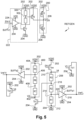
- FIG 3 illustrates, in the form of a circuit, another embodiment of the REFGEN circuit of the figure 1 .
- the REFGEN device is configured to provide only the VrefL voltage.
- the REFGEN device of the figure 3 includes many elements in common with that of the figure 2 , and only the differences between these two devices are highlighted here. In particular, unless otherwise indicated, everything that has been indicated for the REFGEN device described in relation to the figure 2 applies to the REFGEN device of the figure 3 .
- the REFGEN device comprises the voltage divider bridge 200, the resistive voltage divider bridge 208, the buffer circuit BUFFa1, the transistor Ten and the transistor To1.
- Transistor Ten and bridge 208 are connected in series between nodes 202 and 204. However, unlike what has been described in connection with the figure 2 , in figure 3 , transistor Ten is P-channel and has its source connected to node 202, end 212 of divider bridge 208 therefore being connected to node 204.
- output 218 of the buffer circuit BUFFa1 provides the voltage VrefL and not the voltage VrefH as in figure 2 .
- the entrance 218 of the BUFFa1 circuit is connected to an intermediate node of the bridge 208, for example to node 214.
- the source of the transistor To1 is connected to the node 204 and the transistor To1 is N-channel.
- transistor To1 is configured to be in the on state when transistor Ten is in the off state, and to be in the off state when transistor Ten is in the on state. More particularly, transistor To1 is configured so that its on or off state is determined by a voltage value on an intermediate node of the divider bridge 208, for example on node 216 of the bridge 208.
- the REFGEN device comprises the MOS transistor T5 and the resistive element R4 in series between the nodes 202 and 204.
- transistor T5 is N-channel and has its source connected to node 204.
- the divider bridge 200 is configured so that the transistor Ten is in the off state if the voltage VDDE is lower than a threshold VT1, for example substantially equal to 0.9 V, and so that the transistor Ten is on if the voltage VDDE is higher than the threshold VT1. More particularly, the divider bridge 200 is configured to have the above operation when taken alone.
- the REFGEN circuit does not receive the EN-S signal and the VDD voltage.
- the REFGEN device receives the EN-S signal and the VDD voltage.
- the REFGEN device then comprises the circuit 222 configured to receive the EN-S signal and to pull, when the EN-S signal is at its high level, the node 206 to that of the GND potential and the VDDE voltage which controls the blocked state of the transistor Ten.
- circuit 222 is configured to pull node 206 to node 202 when signal EN-S is at its high level.
- the provision of the circuit 222 allows the voltage VrefL to be equal to the voltage of the node 204 to which the source of the transistor To1 is connected.
- the voltage VrefL is at a value allowing the operation of the cascode structures 102 of the IP device ( figure 1 ).
- circuit 222 comprises buffer circuit BUFFn1 and MOS transistor T6.
- transistor T6 is P-channel and has its source connected to node 202, and its gate is not connected to the output of circuit BUFFn1.
- Circuit 222 then further comprises an N-channel MOS transistor T7 and a voltage divider bridge 300 connected in series between nodes 202 and 204.
- Bridge 300 preferably a resistive divider bridge, is connected between node 202 and transistor T7.
- Transistor T7 has its source connected to node 204, its gate connected to the output of circuit BUFFn1 and its drain connected to bridge 300. The gate of transistor T6 is connected to an intermediate node 302 of bridge 300.
- transistor T7 when voltage VDDE is greater than voltage Vmax and signal EN-S is therefore at its low level, transistor T7 then has a zero gate-source voltage but a drain-source voltage equal to VDDE and therefore greater than the voltage withstand Vmax of the transistors of the device IP.
- transistor T7 is chosen to be able to withstand voltage VDDE on its drain.
- transistor T7 is an extended drain transistor.
- the REFGEN device described in relation to the figure 3 has the advantage of being able to be implemented with MOS transistors similar to those of the IP device, i.e. MOS transistors having a voltage withstand Vmax, except for the transistor T7 which is sized to be able to withstand the voltage VDDE on its drain.
- REFGEN device is configured to provide the voltage VrefL, which implies that the transistor To1 has its source connected to the node 204.
- the device described in relation to the figure 3 is configured to generate the voltage VrefH.
- the transistor To1 is P-channel, and has its source connected to the node 202.
- the transistor To1 remains controlled from a voltage on an intermediate node of the bridge 208, for example the node 216, so as to be on when the transistor Ten is off, and to be off when the transistor Ten is on.
- the gate of the transistor To1 is, for example, connected to the node 216, the transistor T5 and the resistive element R4 possibly being omitted.
- the voltage VrefH is then provided on the output of the circuit BUFFa1 in place of the voltage VrefL, the voltage VrefH following the voltage VDDE as long as the transistor Ten is off and being equal to the voltage on the node 214 when the transistor Ten is on.
- bridge 208 is configured so that the voltage on node 214 is equal to 0.55 times voltage VDDE when transistor Ten is on.
- FIG 4 represents, in the form of a circuit, a variant embodiment of the REFGEN circuit of the figure 2 .
- the REFGEN circuit of the figure 4 is configured to generate the voltage VrefH and the voltage VrefL.
- the REFGEN device of the figure 4 includes many elements in common with that of the figure 2 , and only the differences between these two devices are here highlighted. In particular, unless otherwise indicated, all that has been indicated for the REFGEN device described in relation to the figure 2 applies to the REFGEN device of the figure 4 .
- the REFGEN device of the figure 4 further comprises a resistive voltage divider bridge 400 and a MOS transistor T8 in series between nodes 202 and 204.
- the source of transistor T8 is connected to the node 202 and 204 to which the source of transistor Ten is not connected, i.e. to node 202 in the embodiment of the figure 4 .
- transistor T8 is P-channel.
- Transistor T8 is configured to be on, respectively off, when transistor Ten is on, respectively off.
- Transistor T8 has its gate connected to an intermediate node of bridge 208, for example to node 216.
- the divider bridge 400 has one end 402 connected to the drain of the transistor T8.
- the divider bridge 400 has another end 404 connected to the node 204 in the embodiment of the figure 4 .
- the bridge 400 comprises, for example, at least three resistive elements R5, R6 and R7.
- Each resistive element R5, R6, R7 of the bridge 400 may correspond to a single resistor or to a series and/or parallel association of several resistors.
- the element R5 is connected between the end 404 and an intermediate node 406 of the bridge 400
- the element R6 is connected between the node 406 and another intermediate node 408 of the bridge 400
- the element R7 is connected between the node 408 and the end 402 of the bridge 400.
- the REFGEN device of the figure 4 includes a buffer circuit BUFFa2.
- the circuit BUFFa2 is powered by the voltage VDDE.
- the circuit BUFFa2 has one terminal connected to node 202 and one terminal connected to node 204.
- the BUFFa2 circuit is an analog buffer circuit.
- the BUFFa2 circuit is configured to provide on its output 410 a voltage having a value identical to that of a voltage that it receives on its input 412, while ensuring isolation between its input and its output.
- the BUFFa2 circuit is a unity gain follower circuit.
- Input 412 of circuit BUFFa2 is connected to an intermediate node of bridge 400, for example to node 406.
- output 410 of the BUFFa2 circuit provides the voltage VrefL.
- the REFGEN device further comprises a MOS transistor To2.
- the drain of the transistor To2 is connected to the output of the circuit BUFFa2.
- the source of the transistor To2 is connected to the node 204 in the embodiment of the figure 4 where the circuit BUFFa2 is configured to provide the voltage VrefL.
- the source of the transistor To2 and the source of the transistor To1 are connected to respective different nodes among the nodes 202 and 204.
- transistor To2 is N-channel.
- Transistor To2 is configured to be on when transistor T8 is off, and to be off when transistor T8 is on.
- transistor To2 is configured so that its on or off state is determined by a value of voltage V2 on a node of the divider bridge 208, for example on the node 210 of the divider bridge 300
- transistor To1 is configured so that its on or off state is determined by a voltage value V1 on a node of the divider bridge 400, for example on the node 402 of the bridge 400.
- the transistor To1 has its gate coupled, preferably connected, to the node 402, the transistor To2 having its gate connected, preferably connected, to the node 210.
- the REFGEN device comprises a MOS transistor and a resistive element in series between nodes 202 and 204, identical to transistor T5 and element R4 of the figure 2 , and connected together, to bridge 208 and to transistor To1 in the same way as transistor T5 and element R4 in figure 2 .
- the transistor To1 is then not controlled by the voltage V1 of the bridge 400. Compared to the embodiment illustrated in figure 4 , this variant is more cumbersome.
- the REFGEN device comprises a MOS transistor and a resistive element in series between nodes 202 and 204, identical to transistor T5 and element R4 of the figure 3 , and connected together, to bridge 208 and to transistor To1 in the same way as transistor T5 and element R4 in figure 3 .
- the transistor To2 is then not controlled by the voltage V2 of the bridge 208. Compared to the embodiment illustrated in figure 4 , this variant is more cumbersome.
- the REFGEN device comprises the circuit 222 of the figure 2 .
- circuit 222 is omitted.
- the REFGEN device described in relation to the figure 3 has the advantage of being able to be implemented with MOS transistors similar to those of the IP device, i.e. MOS transistors having a voltage withstand Vmax
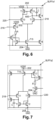
- FIG. 5 represents, in the form of a circuit, a variant embodiment of the REFGEN circuit of the figure 3 .
- the REFGEN circuit of the figure 5 is configured to generate the voltage VrefL and the voltage VrefH.
- the REFGEN device of the figure 5 includes many elements in common with that of the figure 3 , and only the differences between these two devices are highlighted here. In particular, unless otherwise indicated, everything that has been indicated for the REFGEN device described in relation to the figure 3 applies to the REFGEN device of the figure 5 . Furthermore, as the REFGEN device of the figure 5 includes elements described in relation to the REFGEN device of the figure 4 . For these elements, only the differences between the figure 4 and the figure 5 are highlighted.
- the REFGEN device of the figure 5 further includes, as the REFGEN device of the figure 4 , the resistive voltage divider bridge 400 and a MOS transistor T8 in series between nodes 202 and 204.
- the source of transistor T8 is connected to the one of nodes 202 and 204 to which the source of the transistor Ten, i.e. at node 204 in the embodiment of the figure 5 .
- transistor T8 is N-channel.
- Transistor T8 is configured to be on, respectively off, when transistor Ten is on, respectively off.
- transistor T8 has its gate connected to an intermediate node of bridge 208, for example to node 216.
- the divider bridge 400 has its end 404 connected to the node 202 in the embodiment of the figure 4 .
- the REFGEN device of the figure 5 includes, as the REFGEN circuit of the figure 4 , the buffer circuit BUFFa2.
- the input 412 of the circuit BUFFa2 is connected to an intermediate node of the bridge 400, for example to the node 406.
- output 410 of the BUFFa2 circuit provides the voltage VrefH.
- the REFGEN device of the figure 5 further includes, as the REFGEN device of the figure 4 , a MOS transistor To2.
- the source of the transistor To2 is connected to node 202 in the embodiment of the figure 5 where the circuit BUFFa2 is configured to provide the voltage VrefH.
- the source of the transistor To2 and the source of the transistor To1 are connected to different respective nodes among the nodes 202 and 204.
- transistor To2 is P-channel.
- the transistor To2 is configured so that its on or off state is determined by a voltage value V4 on a node of the divider bridge 208, for example on the node 210 of the divider bridge 300
- the transistor To1 is configured so that its on or off state is determined by a voltage value V3 on a node of the divider bridge 400, for example on the node 402 of the bridge 400.
- the transistor To1 has its gate coupled, preferably connected, to the node 402, the transistor To2 having its gate connected, preferably connected, to the node 210.
- the REFGEN device comprises a MOS transistor and a resistive element in series between nodes 202 and 204, identical to transistor T5 and element R4 of the figure 3 , and connected together, to bridge 208 and to transistor To1 in the same way as transistor T5 and element R4 in figure 3 .
- Transistor To1 is then not controlled by voltage V3 of bridge 400. Compared to the embodiment illustrated in figure 5 , this variant is more cumbersome.
- the REFGEN device comprises a MOS transistor and a resistive element in series between nodes 202 and 204, identical to transistor T5 and element R4 of the figure 2 , and connected together, to bridge 208 and to transistor To1 in the same way as transistor T5 and element R4 in figure 2 .
- the transistor To2 is then not controlled by the voltage V4 of the bridge 208.
- this variant is more cumbersome.
- the REFGEN device comprises the circuit 222 of the figure 3 .
- circuit 222 is omitted.
- the REFGEN device described in relation to the figure 3 has the advantage of being able to be implemented with MOS transistors similar to those of the IP device, i.e. MOS transistors having a voltage withstand Vmax, except for the transistor T7 which is sized to be able to withstand the voltage VDDE on its drain.
- FIG 6 represents, in circuit form, an exemplary embodiment of an analog buffer circuit configured to provide the voltage VrefH.
- the buffer circuit described is the BUFFa1 circuit implemented in the REFGEN circuit of the figure 4 .
- the BUFFa1 circuit comprises a differential pair comprising two MOS transistors T10 and T11. Since the BUFFa1 circuit provides the voltage VrefH, the transistors T10 and T11 are preferably N-channel.
- Transistor T10 has its gate connected to input 220 of circuit BUFFa1, and therefore receives, in this example, the voltage present on node 214 of bridge 208 ( figure 4 ).
- Transistor T11 has its gate connected to output 218 of circuit BUFFa1, and therefore receives voltage VrefH.
- the circuit BUFFa1 further comprises two MOS transistors T12 and T13 connected in current mirror of each other, and configured to bias the respective transistors T10 and T11 of the differential pair. Since the circuit BUFFa1 provides the voltage VrefH, the transistors T12 and T13 are preferably P-channel. For example, the transistors T12 and T13 have their sources connected to the node 202 and their gates connected to each other, the gate of the transistor T12 being further connected to the drain of this transistor T12. For example, the drain of the transistor T12, respectively T13, is connected to the drain of the transistor T10, respectively T11.
- the circuit BUFFa1 further comprises a MOS transistor T14 having its gate connected to a node 600 for connecting the transistor T13 to the transistor T11, and its source connected to the output 218 of the circuit. Since the circuit BUFFa1 provides the voltage VrefH, the transistor T14 is preferably N-channel and has its drain connected to the node 202.
- a capacitive element C is connected between the gate and the source of the transistor T14 to improve the stability of the circuit BUFFa1.
- the circuit BUFFa1 further comprises a MOS transistor T15 coupling the differential pair (transistors T10 and T11) to the one of nodes 202 and 204 to which transistors T12 and T13 are not connected, and a MOS transistor T16 coupling the output 218 to the one of nodes 202 and 204 to which transistor T14 is not connected.
- transistors T15 and T16 are therefore N-channel.
- transistors T15 and T16 have their sources connected to node 204, transistor T15 has its drain coupled, preferably connected, to the sources of transistors T10 and T11 of the differential pair, and transistor T16 has its drain coupled, preferably connected, to output 218.
- the circuit BUFFa1 further comprises a MOS transistor T17 with a channel of the same type as that of the channels of the transistors T15 and T16, namely N-channel in this example.
- This transistor T17 has its source connected to the same node, 204 in this example, as the node to which the sources of the transistors T15 and T16 are connected.
- the transistors T15 and T16 are mounted in current mirror with the transistor T17.
- the gates of transistors T15 and T16 are each connected to the gate of transistor T17, the gate of transistor T17 being further connected to the drain of transistor T17.
- the transistor T17 is advantageously biased from an intermediate node of the resistive divider bridge to which the circuit BUFFa1 is connected, namely from an intermediate node of the bridge 208 in this example, for example from the node 216 of the bridge 208 ( figure 4 ).
- the circuit BUFFa1 comprises a MOS transistor T18 with a channel of the opposite type to that of the channel of the transistor T17, and having its source connected to that of the nodes 202 and 204 to which the transistor T17 is not connected.
- the transistor T18 is P-channel and has its source connected to the node 202.
- the gate of the transistor T18 is connected to the intermediate node 216 of the bridge 208 from which the transistor T17 is biased.
- a resistor R couples the drains of the transistors T17 and T18 together.
- the transistor T17 can be biased other than from a node of the resistive divider bridge to which the input 220 of the circuit BUFFa1 is connected.
- the BUFFa1 circuit comprises a MOS transistor T19 with a channel of the same type as that of transistor T17, namely N-channel in this example.
- Transistor T19 is configured to short-circuit transistor T17 when transistor Ten ( figure 4 ) is blocked.
- transistor T19 has its source, respectively its drain, connected to the source, respectively to the drain, of transistor T17.
- the gate of transistor T19 is coupled, preferably connected, to the drain of the transistor which is in series with the resistive divider bridge to which input 220 of circuit BUFFa1 is connected, i.e. to the drain of transistor Ten in this example.
- the BUFFa2 circuit of the figure 5 can be implemented by the circuit described in relation to the figure 6 .
- the gate of transistor T10 is connected to node 406 of bridge 400
- the gate of transistor T18 is connected to a node of bridge 400, for example to node 408, and the gate of transistor T19 is connected to the drain of transistor T8.
- FIG 7 represents, in circuit form, an example of an embodiment of an analog buffer circuit configured to provide the voltage VrefL.
- the buffer circuit described is the BUFFa2 circuit implemented in the REFGEN circuit of the figure 4 .
- the BUFFa2 circuit of the figure 7 is similar to the BUFFa1 circuit of the figure 6 and includes many elements in common with the latter, only the differences between these two devices being highlighted here.
- the transistors T10 and T11 of the BUFFa2 circuit are preferably P-channel.
- the transistor T10 here has its gate connected to input 220 of the circuit BUFFa2, and therefore receives, in this example, the voltage present on node 406 of bridge 400 ( figure 4 ). Furthermore, transistor T11 here has its gate connected to output 218 of circuit BUFFa2, and therefore receives voltage VrefL.
- the transistors T12 and T13 connected in current mirror one of the other to bias the respective transistors T10 and T11 of the differential pair are preferably N-channel.
- transistors T12 and T13 here have their sources connected to node 204 and their gates connected to each other, the gate of transistor T12 being further connected to the drain of this transistor T12.
- the drain of transistor T12, respectively T13 is connected to the drain of transistor T10, respectively T11.
- the transistor T14 having its gate connected to the node 600 and its source connected to the output 218 of the circuit BUFFa2 is, preferably, P-channel and has its drain connected to the node 202.
- the BUFFa2 circuit includes the capacitive element C connected between the gate and the source of the transistor T14 to improve its stability.
- transistors T15 and T16 are connected to node 202.
- Transistor T15 therefore couples the differential pair to node 202, and, in addition, transistor T16 therefore couples output 218 to node 202.
- transistors T15 and T16 are therefore P-channel.
- transistors T15 and T16 have their sources connected to node 202, transistor T15 has its drain coupled, preferably connected, to the sources of transistors T10 and T11, and transistor T16 has its drain coupled, preferably connected, to output 218.
- Transistor T17 with a channel of the same type as that of the channels of transistors T15 and T16 is therefore P-channel in circuit BUFFa2, and has its source connected to the same node, 202 in this example, as the node to which the sources of transistors T15 and T16 are connected.
- Transistors T15 and T16 are connected in current mirror with transistor T17.
- the transistor T17 is advantageously biased from an intermediate node of the resistive divider bridge to which the circuit BUFFa2 is connected, namely from an intermediate node of the bridge 400 in this example, for example from the node 406 of the bridge 400 ( figure 4 ).
- the circuit BUFFa2 comprises the MOS transistor T18 with a channel of the opposite type to that of the channel of the transistor T17, and having its source connected to that of the nodes 202 and 204 to which the transistor T17 is not connected.
- the transistor T18 is N-channel and has its source connected to the node 204.
- the gate of the transistor T18 is connected to the intermediate node 406 of the bridge 400 from which the transistor T17 is biased.
- the resistor R couples the drains of the transistors T17 and T18 together.
- the transistor T17 can be biased other than from a node of the resistive divider bridge to which the input 220 of the circuit BUFFa2 is connected.
- the BUFFa2 circuit comprises a MOS transistor T19 with a channel of the same type as that of transistor T17, namely P-channel in this example.
- Transistor T19 is configured to short-circuit transistor T17 when transistor Ten ( figure 4 ) is blocked.
- transistor T19 has its source, respectively its drain, connected to the source, respectively to the drain, of transistor T17.
- transistor T19 For transistor T19 to be on when transistor Ten is blocked, the gate of transistor T19 is coupled, preferably connected, to the drain of the transistor which is in series with the divider bridge resistive to which input 220 of the BUFFa2 circuit is connected, that is to say to the drain of transistor T8 in this example.
- the BUFFa1 circuit of the figure 5 can be implemented by the circuit described in relation to the figure 7 .
- the gate of transistor T10 of the circuit of the figure 7 is connected to node 214 of bridge 208
- the gate of transistor T18 is connected to a node of bridge 208, for example to node 216
- the gate of transistor T19 is connected to the drain of transistor Ten.
- each of the voltages VrefH and VrefL is generated from the voltage VDDE.
- each of the voltages VrefH and VrefL follows the variations of the voltage VDDE, and, in particular, the overvoltages or undervoltages of the voltage VDDE. This makes it possible to keep the voltages across the cascode transistors T2 and T3 of the structures 100 and 102 at values lower than the voltage withstand limit Vmax of these transistors.
- each of the voltages VrefH and VrefL follows the variations of the voltage VDDE and is not generated from the voltage VDD, there is no longer any constraint on the order in which the supply voltages VDDE and VDD must be provided.
- each of the voltages VrefH and VrefL is generated from the voltage VDDE by a corresponding resistive voltage divider bridge 208 or 400.
- the dependence of the current value of each of the voltages VrefL and VrefH on the temperature is reduced or eliminated.
- the ratio between the current value of the voltage VrefH, respectively VrefL, and that of the voltage VDDE can be easily chosen by adapting the values of one or more of the resistive elements of the corresponding bridge 208 or 400.
Landscapes
- Engineering & Computer Science (AREA)
- Physics & Mathematics (AREA)
- Electromagnetism (AREA)
- General Physics & Mathematics (AREA)
- Radar, Positioning & Navigation (AREA)
- Automation & Control Theory (AREA)
- Power Engineering (AREA)
- Microelectronics & Electronic Packaging (AREA)
- Nonlinear Science (AREA)
- Control Of Electrical Variables (AREA)
Applications Claiming Priority (1)
| Application Number | Priority Date | Filing Date | Title |
|---|---|---|---|
| FR2304777A FR3148849A1 (fr) | 2023-05-15 | 2023-05-15 | Circuit de génération de tension de référence |
Publications (1)
| Publication Number | Publication Date |
|---|---|
| EP4465146A1 true EP4465146A1 (de) | 2024-11-20 |
Family
ID=87571413
Family Applications (1)
| Application Number | Title | Priority Date | Filing Date |
|---|---|---|---|
| EP24174416.8A Pending EP4465146A1 (de) | 2023-05-15 | 2024-05-07 | Referenzspannungserzeugungsschaltung |
Country Status (3)
| Country | Link |
|---|---|
| US (1) | US20240385636A1 (de) |
| EP (1) | EP4465146A1 (de) |
| FR (1) | FR3148849A1 (de) |
Families Citing this family (1)
| Publication number | Priority date | Publication date | Assignee | Title |
|---|---|---|---|---|
| CN119512290A (zh) * | 2023-08-23 | 2025-02-25 | 联发科技(新加坡)私人有限公司 | 一种动态偏置电压电路及集成电路 |
Citations (1)
| Publication number | Priority date | Publication date | Assignee | Title |
|---|---|---|---|---|
| CN102455728A (zh) * | 2010-10-25 | 2012-05-16 | 三星半导体(中国)研究开发有限公司 | 电流控制电路 |
Family Cites Families (2)
| Publication number | Priority date | Publication date | Assignee | Title |
|---|---|---|---|---|
| US8816655B2 (en) * | 2010-10-25 | 2014-08-26 | Samsung Electronics Co., Ltd. | Voltage regulator having soft starting function and method of controlling the same |
| KR20220075631A (ko) * | 2020-11-30 | 2022-06-08 | 삼성전자주식회사 | 전자 장치 |
-
2023
- 2023-05-15 FR FR2304777A patent/FR3148849A1/fr active Pending
-
2024
- 2024-05-07 US US18/657,462 patent/US20240385636A1/en active Pending
- 2024-05-07 EP EP24174416.8A patent/EP4465146A1/de active Pending
Patent Citations (1)
| Publication number | Priority date | Publication date | Assignee | Title |
|---|---|---|---|---|
| CN102455728A (zh) * | 2010-10-25 | 2012-05-16 | 三星半导体(中国)研究开发有限公司 | 电流控制电路 |
Also Published As
| Publication number | Publication date |
|---|---|
| FR3148849A1 (fr) | 2024-11-22 |
| US20240385636A1 (en) | 2024-11-21 |
Similar Documents
| Publication | Publication Date | Title |
|---|---|---|
| EP0594834B1 (de) | In Standard-CMOS-Technologie realisierte, zwischen einer Logikschaltung mit niedriger Versorgungsspannung und einer Ausgangsstufe mit hoher Versorgungsspannung, liegende Schaltung | |
| FR2814608A1 (fr) | Circuit d'amplificateur operationnel | |
| EP2458849B1 (de) | Detektionsschaltung mit doppelter korrelierter Signalabtastung und verbesserter Überlaufsvorrichtung | |
| EP0675422B1 (de) | Regelschaltung zur Erzeugung einer temperatur- und versorgungsspannungsunabhängigen Referenzspannung | |
| EP4465146A1 (de) | Referenzspannungserzeugungsschaltung | |
| FR2678451A1 (fr) | Circuit d'attaque de sortie cmos a puits flottant. | |
| FR2957732A1 (fr) | Etage de sortie d'un circuit electronique | |
| EP0022015A1 (de) | Audioverstärker und Verfahren zur Audiofrequenzverstärkung | |
| EP0738038A1 (de) | Stromverstärker | |
| EP1249707A1 (de) | Schaltung zur Ermittlung einer Versorgung | |
| FR3119469A1 (fr) | Interface USB PD | |
| FR3058857A1 (fr) | Capteur d'images cmos a bruit reduit | |
| EP1313309A1 (de) | Kalibriervorrichtung für eine Video-Eingangsstufe | |
| FR3134487A1 (fr) | Dispositif de copie d'un courant | |
| EP4513757A1 (de) | Vorrichtung zur überwachung einer oder mehrerer stromversorgungen | |
| EP4030621B1 (de) | Dynamischer komparator | |
| EP4012924B1 (de) | Dynamischer komparator | |
| FR2818762A1 (fr) | Regulateur de tension a gain statique en boucle ouverte reduit | |
| EP0836272B1 (de) | Rauscharme Verstärkungsanordnung | |
| FR3115426A1 (fr) | Amplificateur opérationnel | |
| EP4517473B1 (de) | Spannungsregler | |
| FR3103333A1 (fr) | Dispositif pour générer un courant | |
| EP0608938A1 (de) | Verstärker mit Differenzeingangsstufe und integrierter Stabilisierungskapazität | |
| EP4178218B1 (de) | Pixel für infrarot-bildgeber mit bdi-vorspannung und aktiver rücksetzung | |
| EP1569332B1 (de) | Leistungsverstärker und Operationsverstärker, der diesen beinhaltet |
Legal Events
| Date | Code | Title | Description |
|---|---|---|---|
| PUAI | Public reference made under article 153(3) epc to a published international application that has entered the european phase |
Free format text: ORIGINAL CODE: 0009012 |
|
| STAA | Information on the status of an ep patent application or granted ep patent |
Free format text: STATUS: REQUEST FOR EXAMINATION WAS MADE |
|
| 17P | Request for examination filed |
Effective date: 20240507 |
|
| AK | Designated contracting states |
Kind code of ref document: A1 Designated state(s): AL AT BE BG CH CY CZ DE DK EE ES FI FR GB GR HR HU IE IS IT LI LT LU LV MC ME MK MT NL NO PL PT RO RS SE SI SK SM TR |