EP4513757A1 - Vorrichtung zur überwachung einer oder mehrerer stromversorgungen - Google Patents
Vorrichtung zur überwachung einer oder mehrerer stromversorgungen Download PDFInfo
- Publication number
- EP4513757A1 EP4513757A1 EP24193599.8A EP24193599A EP4513757A1 EP 4513757 A1 EP4513757 A1 EP 4513757A1 EP 24193599 A EP24193599 A EP 24193599A EP 4513757 A1 EP4513757 A1 EP 4513757A1
- Authority
- EP
- European Patent Office
- Prior art keywords
- transistor
- voltage
- node
- circuit
- vdde
- Prior art date
- Legal status (The legal status is an assumption and is not a legal conclusion. Google has not performed a legal analysis and makes no representation as to the accuracy of the status listed.)
- Pending
Links
Images



Classifications
-
- H—ELECTRICITY
- H03—ELECTRONIC CIRCUITRY
- H03K—PULSE TECHNIQUE
- H03K17/00—Electronic switching or gating, i.e. not by contact-making and –breaking
- H03K17/22—Modifications for ensuring a predetermined initial state when the supply voltage has been applied
- H03K17/223—Modifications for ensuring a predetermined initial state when the supply voltage has been applied in field-effect transistor switches
-
- G—PHYSICS
- G06—COMPUTING OR CALCULATING; COUNTING
- G06F—ELECTRIC DIGITAL DATA PROCESSING
- G06F1/00—Details not covered by groups G06F3/00 - G06F13/00 and G06F21/00
- G06F1/24—Resetting means
-
- H—ELECTRICITY
- H03—ELECTRONIC CIRCUITRY
- H03K—PULSE TECHNIQUE
- H03K2217/00—Indexing scheme related to electronic switching or gating, i.e. not by contact-making or -breaking covered by H03K17/00
- H03K2217/0036—Means reducing energy consumption
Definitions
- a supply voltage When a supply voltage is turned off, it is in a high impedance state. When it is turned on, or powered up, this supply voltage first has a zero value before reaching its nominal or target value following a ramp-up phase. When turning on and ramping up one or more supply voltages of a portion of the chip, many problems arise in the circuits that receive this or these supply voltages to be powered.
- Known circuits generate, when one or more supply voltages are increased, a reset signal which makes it possible to put the circuits to be supplied with this or these supply voltages in a known initial state.
- a power-on reset device that provides a reset signal having a defined state whenever one of the supply voltages monitored by the device is turned on and is no longer in a high impedance state.
- the circuit further comprises a capacitive element connected between the gate and the source of the first transistor.
- the circuit further comprises a second CMOS inverter configured to be powered by the second voltage, an input of the second inverter being connected to the output of the first inverter, and an output of the second inverter being configured to provide a signal complementary to the reset signal.
- the first and second resistive elements, and the first and fourth transistors are sized such that the fourth transistor is blocked when the first transistor is on.
- the second voltage is also a supply voltage.
- the CMOS logic gate is configured to be powered by the second voltage provided by the voltage generation circuit.
- the voltage generation circuit is configured to provide the second reference DC voltage at its nominal value before powering up and ramping up each of the first voltages.
- the expressions “approximately”, “approximately”, “substantially”, and “of the order of” mean to within 10%, preferably to within 5%.
- the circuit 1000 is configured to provide a reset signal POR to a low binary state corresponding, for example, to a zero voltage when a circuit to be supplied with two supply voltages VDDE and VDD must be reset, and to a high binary state corresponding, for example, to a voltage of value equal to the nominal value of the voltage VDEE when the rise in power of the two voltages VDDE and VDD is complete, that is to say when these two voltages VDDE and VDD have reached their respective nominal values.
- the low state of the signal POR causes the reset of the circuit to be supplied with the voltages VDD and VDDE and this reset phase ends when all the voltages have completed their rises in power and the signal POR switches to the high state.
- the circuit 1000 is powered by the voltage VDDE or VDD which has the highest nominal value, namely VDDE in this example.
- the circuit 1000 comprises a node (or rail) 1004 configured to receive the voltage VDDE, and a node (or rail) 1006 configured to receive a reference potential GND, for example ground.
- the circuit 1000 comprises a logic gate 1002 implemented in CMOS technology (from the English "Complementary MOS” - complementary MOS), i.e. a CMOS 1002 logic gate. Gate 1002 is powered by voltage 1002.
- Gate 1002 includes as many PMOS transistors P1 as it has inputs, i.e. two transistors P1 in this example.
- the transistors P1 are connected in parallel between nodes 1004 and 1008.
- Each transistor P1 has its gate connected to a different input of gate 1002.
- a first transistor P1 has its gate connected to voltage VDD, or, in other words, has its gate configured to receive voltage VDD
- a second transistor P1 has its gate connected to voltage VDDE or, in other words, has its gate configured to receive voltage VDDE.
- gate 1002 includes as many NMOS transistors N1 as it has inputs, i.e. two transistors N1 in this example.
- the transistors N1 are connected in series between nodes 1008 and 1006.
- Each transistor N1 has its gate connected to a different input of gate 1002.
- a first transistor N1 has its gate connected to voltage VDD
- a second transistor N1 has its gate connected to voltage VDDE.
- the inverter INV1 is implemented in CMOS technology. More particularly, the inverter INV1 comprises a PMOS transistor P2 connected between node 1004 and output 1010 and having its gate connected to node 1008, and an NMOS transistor N2 connected between output 1010 and node 1006 and having its gate connected to node 1008.
- the circuit 1000 further comprises an inverter INV2.
- the inverter INV2 is powered by the voltage VDDE.
- the inverter INV2 is implemented in CMOS technology.
- the inverter INV2 has an input connected to the output 1010 of the inverter INV1, and an output 1012 configured to provide an nPOR signal complementary to the POR signal.
- the inverter INV2 comprises a PMOS transistor P3 connected between the node 1004 and the output 1012 and having its gate connected to the node 1010, and an NMOS transistor N3 connected between the output 1012 and the node 1006 having its gate connected to the node 1010.
- circuit 1000 monitoring the rise in power of two supply voltages VDDE and VDD has been described here, the person skilled in the art is able to adapt this example to the case where the circuit 1000 monitors the rise in power of more than two supply voltages, by increasing the number of inputs of the gate 1002.
- the output 1008 is in a high impedance state, just like the POR signal.
- circuit 1000 at the end of the ramp-up of all the supply voltages that it monitors, if one of the monitored voltages, for example voltage VDD, has a different and lower nominal value than that of voltage VDDE, then the circuit consumes energy which is proportional to the difference between these nominal values, which is not desirable.
- the circuit 1000 is therefore not suitable for use as a power-on reset circuit for a RRAM (Resistive Random Access Memory) type memory powered by the voltages VDD and VDDE having, for example, nominal values respectively substantially equal to 1.8 V and 3.3 V.
- RRAM Resistive Random Access Memory
- this alternative circuit has advantages over circuit 1000, it is difficult to adapt this alternative power-on reset circuit to examples where more than two supply voltages are monitored. Furthermore, this alternative power-on reset circuit has at least some of the disadvantages of circuit 1000, such as a static consumption at the end of the ramp-up of voltages VDDE and VDD that is proportional to the difference between these two voltages.
- FIG. 2 represents an embodiment of a power-on reset circuit 2000.
- the circuit 2000 comprises a node 2002 configured to receive the reference potential GND, a node 2004 configured to receive a first direct voltage V1, the first direct voltage being a supply voltage monitored by the circuit 2000, and a node 2006 to receive another direct voltage V2.
- Circuit 2000 includes an NMOS transistor MN1.
- Transistor MN1 has its gate connected to node 2004.
- the circuit 2000 includes an NMOS transistor MN2.
- the drain of transistor MN2 is connected to the source of transistor MN1 and the source of transistor MN2 is connected to node 2004.
- Circuit 2000 includes an NMOS transistor MN3.
- the gate of transistor MN3 is connected to node 2004 and the source of transistor MN3 is connected to node 2002.
- Circuit 2000 includes a PMOS transistor MP3.
- the drain of transistor MP3 is connected to the drain of transistor MN3, the drain of transistor MN3 being connected to the gate of transistor MN2.
- the gate of transistor MP3 is connected to the source of transistor MN1.
- circuit 2000 includes resistive element 2008 connected between the drain of transistor MN1 and node 2006.
- resistive element 2008 has a terminal connected to the drain of transistor MN1 and a terminal connected to node 2006.
- Circuit 2000 also includes resistive element 2010 connected between the source of transistor MP3 and node 2006.
- resistive element 2010 has a terminal connected to the source of transistor MP3 and a terminal connected to node 2006.
- the circuit 2000 comprises an inverter INV3 implemented in CMOS technology.
- the inverter INV3 is powered by the voltage V2, and, more generally, the circuit 2000 is powered by the voltage V2.
- An input of the inverter INV3 is connected to the drain of the transistor MP3, therefore to the drain of the transistor MN3 and to the gate of the transistor MN2.
- the output 2012 of the inverter INV3 is configured to provide a reset signal POR2000 on power-up.
- inverter INV3 comprises a PMOS transistor P4 connected between node 2006 and output 2012 and having its gate connected to the drains of transistors MP3 and MN3, and an NMOS transistor N4 connected between output 1012 and node 2002 and having its gate connected to the drains of transistors MP3 and MN3.
- the circuit 2000 comprises an optional capacitive element Ce connected between the gate and the source of the transistor MN1.
- the circuit 2000 when the circuit 2000 is configured to provide, in addition to the circuit POR2000 on the output 2012 of the inverter INV3 which is also an output of the circuit 2000, a signal nPOR2000 complementary to the signal POR2000, the circuit 2000 comprises an inverter INV4 implemented in CMOS technology.
- the inverter INV4 is powered by the voltage V2.
- An input of the inverter INV4 is connected to the output 2012 of the inverter INV3, and an output 2014 of the inverter INV4 is configured to provide the signal nPOR2000.
- inverter INV4 includes a PMOS transistor P5 connected between node 2006 and output 2014 and having its gate at output 2012, and an NMOS transistor N5 connected between output 1014 and node 2002 and having its gate connected to output 2012.
- each of the resistive elements 2008 and 2010 is implemented by a respective PMOS transistor having its gate connected to the node 2002 so as to receive the potential GND and its source connected to the node 2006.
- the resistive element 2008 is implemented by a PMOS transistor MP1 having its gate controlled by the potential GND, its source connected to the node 2006 and its drain connected to the drain of the transistor MN1
- the resistive element 2010 is implemented by a PMOS transistor MP2 having its gate controlled by the potential GND, its source connected to the node 2006 and its drain connected to the source of the transistor MP3.
- An advantage of implementing the 2008 and 2010 resistive elements with the PMOS transistors MP1 and MP2 rather than with resistors is that, for a footprint similarly, the resistive elements will have greater resistance values, which allows to reduce the static consumption of the circuit 2000 compared to the case where these resistive elements would have been implemented with resistors.
- the resistive elements 2008 and 2010 are implemented with resistors.
- the voltage on the gate of the transistor MP3 follows the increase in the voltage V1.
- the voltage on the gate of the transistor MP3 then becomes equal to the voltage V2 minus the voltage drops across the resistive element 2008 and at the terminals of the transistor MN1, and, on the other hand, the voltage on the gate of the transistor MN2 is pulled towards the potential GND.
- voltage V1 corresponds to one of the supply voltages of a circuit to be supplied to which a reset signal must be provided in a defined state as soon as one of its supply voltages is switched on
- the voltage V2 is a reference voltage VrefH having a non-zero value, preferably its nominal value, before the switching on and the power ramping up of each of the supply voltages of the circuit to be supplied.
- the circuit 2000 can monitor only one of the supply voltages of the circuit to be supplied.
- a reset device is proposed on switching on comprising several circuits 2000, an exemplary embodiment of which will now be described in relation to the figure 3 .
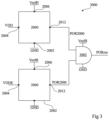
- FIG. 3 represents an embodiment of a power-on reset device 3000.
- the device 3000 comprises as many circuits 2000 as it monitors supply voltages.
- the circuit 3000 comprises two circuits 2000.
- the person skilled in the art is able to adapt the description given for the case where the device 3000 monitors only the two voltages VDD and VDDE to the case where the device 3000 monitors more than three supply voltages.
- the 2002 nodes of the 2000 circuits all receive the same GND reference potential.
- the nodes, or inputs, 2004 of the circuits 2000 each receive a supply voltage to be monitored which is part of the supply voltages monitored by the device 3000 and which is different from the supply voltages to be monitored received by the nodes 2004 of the other circuits 2000.
- the device 3000 monitors the two voltages VDD and VDDE
- one of the two circuits 2000 receives the voltage VDD on its node 2004, and the other of the two circuits 2000 (at the bottom in figure 3 ) receives the VDDE voltage on its node 2004.
- the device 3000 comprises a logic gate 3002 implemented in CMOS technology and powered by the reference voltage VrefH. More particularly, the logic gate 3002 implements a Boolean AND logic function between the signals POR2000 provided by the circuits 2000. In the example of the figure 3 , gate 3002 therefore includes two inputs receiving the POR2000 signals from the two circuits 2000. The output of gate 3002 provides the PORres initialization signal at power-up which will be provided to the circuit to be supplied with the voltages VDD and VDDE which the device 3000 monitors.
- the reference voltage generation circuit is configured to provide the reference DC voltage VrefH at its nominal value before a power-up and a ramp-up of each of the voltages VDD and VDDE monitored by the device 3000.
- the reference voltage generation circuit is a band-hopping type circuit.
- the circuit 2000 receiving on its node 2004 the voltage that has just been switched on will provide a POR2000 signal in the low state.
- the low state of at least one POR2000 signal causes the PORres signal to be in the low state.
- the PORres signal remains in its low state.
- the device 3000 therefore makes it possible to monitor the voltages VDDE and VDD and to provide an initialization signal PORres on power-up which is in a defined low state as soon as one of the voltages VDDE and VDD is switched on, and which then only switches to its high state when all the monitored voltages VDD and VDDE have finished their power increases, which was not the case with the circuit 1000 of the figure 1 .
- the PORres signal is then independent of the sequence in which the monitored voltages are switched on and ramped up.
- the circuit to be supplied with the voltages VDDE and VDD comprises cascode structures each supplied with the voltage VDDE, and each comprising a transistor having its gate biased by the voltage VrefH and a transistor having its gate controlled by a binary signal.
- the circuit for generating the voltage VrefH is configured so that the voltage VrefH allows an implementation of the cascode structures with transistors whose voltage withstand Vmax is lower than values that the difference between the voltages VDDE and VDD can take while the ignition sequence of the voltages VDDE and VDD is not imposed.
- the voltage VrefH for biasing the cascode structures can advantageously serve as the VrefH voltage for the 2000 circuits previously described.
- the device comprises a voltage generation circuit configured to provide the voltage V2, such that the voltage V2 is non-zero before a power-up and a ramp-up of the voltage V1.
- a voltage generation circuit configured to provide the voltage V2, such that the voltage V2 is non-zero before a power-up and a ramp-up of the voltage V1.
- First examples have been described in which, when the voltage V1 is powered up and ramps up, the voltage V2 is already at its nominal value, that is to say, for example, that the ramp-up of the voltage V2 has finished.
- second examples have been described in which when the voltage V1 is powered up and ramps up, the voltage V2 is at a non-zero value, which may be different from its nominal value, for example, when the voltage V2 has not finished ramping up when that of the voltage V1 begins.
- the voltage V2 may depend on a supply voltage, for example VDDE, the ramp-up of which is not finished when the voltage V1 begins ramping up.
- VDDE supply voltage
- voltage V2 when voltage V1 begins its power increase, voltage V2 may have a non-zero value that varies with that of the supply voltage on which it depends, until voltage V2 reaches its nominal value.
- voltage V2 is, for example, supplied by the circuit of Figures 4 to 10 described below.
- the voltage V2 has a non-zero value, nominal or not, adapted to allow the switching of the transistor MP3 to the on state as soon as the voltage V1 is switched on and the start of its power rise, such that the signal on the drain of the transistor MP3 is in a determined state from the start of this power rise of the voltage V1.
- the non-zero value of the voltage V2 is further adapted to allow the operation of the inverter INV3 such that the signal POR2000 is in a defined state and not in a high impedance state, for example adapted to allow the operation of the inverters INV3 and INV4 such that the signals POR2000 and nPOR200 are in defined states and not in high impedance states.
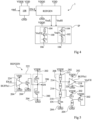
- FIG. 4 represents, schematically and in the form of blocks, an example of an electronic system 1 comprising a REFGEN device for generating a reference voltage according to one embodiment.
- the system corresponding for example to a portion of an integrated circuit chip, comprises an IP device, for example a resistive memory, and the REFGEN device.
- IP device for example a resistive memory
- REFGEN device for example a resistive memory
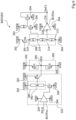
- the REFGEN device of the figure 7 further comprises a resistive voltage divider bridge 400 and a MOS transistor T8 in series between nodes 202 and 204.
- the divider bridge 400 has one end 402 connected to the drain of the transistor T8.
- the divider bridge 400 has another end 404 connected to the node 204 in the embodiment of the figure 7 .
- the bridge 400 comprises, for example, at least three resistive elements R5, R6 and R7.
- Each resistive element R5, R6, R7 of the bridge 400 may correspond to a single resistor or to a series and/or parallel association of several resistors.
- the element R5 is connected between the end 404 and an intermediate node 406 of the bridge 400
- the element R6 is connected between the node 406 and another intermediate node 408 of the bridge 400
- the element R7 is connected between the node 408 and the end 402 of the bridge 400.
- the REFGEN device of the figure 7 includes a buffer circuit BUFFa2.
- the BUFFa2 circuit is powered by the voltage VDDE.
- the BUFFa2 circuit has one terminal connected to node 202 and one terminal connected to node 204.
- Input 412 of circuit BUFFa2 is connected to an intermediate node of bridge 400, for example to node 406.
- output 410 of the BUFFa2 circuit provides the voltage VrefL.
- the REFGEN device further comprises a MOS transistor To2.
- the drain of the transistor To2 is connected to the output of the circuit BUFFa2.
- the source of the transistor To2 is connected to the node 204 in the embodiment of the figure 7 where the circuit BUFFa2 is configured to provide the voltage VrefL.
- the source of the transistor To2 and the source of the transistor To1 are connected to different respective nodes among the nodes 202 and 204.
- transistor To2 is N-channel.
- the transistor To2 is configured so that its on or off state is determined by a voltage value V2 on a node of the divider bridge 208, for example on the node 210 of the divider bridge 300
- the transistor To1 is configured so that its on or off state is by a voltage value V1 on a node of the divider bridge 400, for example on the node 402 of the bridge 400.
- the transistor To1 has its gate coupled, preferably connected, to the node 402, the transistor To2 having its gate coupled, preferably connected, to the node 210.
- the REFGEN device comprises a MOS transistor and a resistive element in series between nodes 202 and 204, identical to transistor T5 and element R4 of the figure 6 , and connected together, to bridge 208 and to transistor To1 in the same way as transistor T5 and element R4 in figure 6 .
- the transistor To2 is then not controlled by the voltage V2 of the bridge 208. Compared to the embodiment illustrated in figure 7 , this variant is more cumbersome.
- the REFGEN device comprises the circuit 222 of the figure 4 .
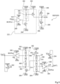
- FIG 8 represents, in the form of a circuit, a variant embodiment of the REFGEN circuit of the figure 6 .
- the REFGEN circuit of the figure 8 is configured to generate the voltage VrefL and the voltage VrefH.
- the REFGEN device of the figure 8 further includes, as the REFGEN device of the figure 7 , the resistive voltage divider bridge 400 and a MOS transistor T8 in series between nodes 202 and 204.
- the divider bridge 400 has its end 404 connected to the node 202 in the embodiment of the figure 8 .
- the REFGEN device of the figure 8 includes, as the REFGEN circuit of the figure 7 , the buffer circuit BUFFa2.
- the input 412 of the circuit BUFFa2 is connected to an intermediate node of the bridge 400, for example to the node 406.
- output 410 of the BUFFa2 circuit provides the voltage VrefH.
- the transistor To2 is configured so that its on or off state is determined by a voltage value V4 on a node of the divider bridge 208, for example on the node 210 of the divider bridge 300
- the transistor To1 is configured so that its on or off state is determined by a voltage value V3 on a node of the divider bridge 400, for example on the node 402 of the bridge 400.
- the transistor To1 has its gate coupled, preferably connected, to the node 402, the transistor To2 having its gate coupled, preferably connected, to the node 210.
- the REFGEN device comprises a MOS transistor and a resistive element in series between nodes 202 and 204, identical to transistor T5 and element R4 of the figure 3 , and connected between them, to bridge 208 and to transistor To1 in the same way as transistor T5 and element R4 in figure 6 .
- Transistor To1 is then not controlled by voltage V3 of bridge 400. Compared to the embodiment illustrated in figure 8 , this variant is more cumbersome.
- the REFGEN device comprises a MOS transistor and a resistive element in series between nodes 202 and 204, identical to transistor T5 and element R4 of the figure 5 , and connected together, to bridge 208 and to transistor To1 in the same way as transistor T5 and element R4 in figure 5 .
- the transistor To2 is then not controlled by the voltage V4 of the bridge 208.
- this variant is more cumbersome.
- the REFGEN device comprises the circuit 222 of the figure 6 .
- circuit 222 is omitted.
- the REFGEN device described in relation to the figure 8 has the advantage of being able to be implemented with MOS transistors similar to those of the IP device, i.e. MOS transistors having a voltage withstand Vmax, except for the transistor T7 which is sized to be able to withstand the voltage VDDE on its drain.
- the 2000 circuits can then also be implemented with MOS transistors having a voltage withstand Vmax.
- FIG 9 represents, in circuit form, an exemplary embodiment of an analog buffer circuit configured to provide the voltage VrefH.
- the buffer circuit described is the BUFFa1 circuit implemented in the REFGEN circuit of the figure 7 .
- the BUFFa1 circuit comprises a differential pair comprising two MOS transistors T10 and T11. Since the BUFFa1 circuit provides the voltage VrefH, the transistors T10 and T11 are preferably N-channel.
- Transistor T10 has its gate connected to input 220 of circuit BUFFa1, and therefore receives, in this example, the voltage present on node 214 of bridge 208 ( figure 7 ).
- Transistor T11 has its gate connected to output 218 of circuit BUFFa1, and therefore receives voltage VrefH.
- the circuit BUFFa1 further comprises two MOS transistors T12 and T13 mounted in current mirror of each other, and configured to bias the respective transistors T10 and T11 of the differential pair. Since the circuit BUFFa1 provides the voltage VrefH, the transistors T12 and T13 are preferably P-channel. For example, the transistors T12 and T13 have their sources connected to the node 202 and their gates connected to each other, the gate of the transistor T12 being further connected to the drain of this transistor T12. For example, the drain of the transistor T12, respectively T13, is connected to the drain of the transistor T10, respectively T11.
- the circuit BUFFa1 further comprises a MOS transistor T14 having its gate connected to a node 600 for connecting the transistor T13 to the transistor T11, and its source connected to the output 218 of the circuit. Since the circuit BUFFa1 provides the voltage VrefH, the transistor T14 is preferably N-channel and has its drain connected to the node 202.
- a capacitive element C is connected between the gate and the source of the transistor T14 to improve the stability of the circuit BUFFa1.
- the circuit BUFFa1 further comprises a MOS transistor T15 coupling the differential pair (transistors T10 and T11) to the one of nodes 202 and 204 to which transistors T12 and T13 are not connected, and a MOS transistor T16 coupling the output 218 to the one of nodes 202 and 204 to which transistor T14 is not connected.
- transistors T15 and T16 are therefore N-channel.
- transistors T15 and T16 have their sources connected to node 204, transistor T15 has its drain coupled, preferably connected, to the sources of transistors T10 and T11 of the differential pair, and transistor T16 has its drain coupled, preferably connected, to output 218.
- the circuit BUFFa1 further comprises a MOS transistor T17 with a channel of the same type as that of the channels of the transistors T15 and T16, namely N-channel in this example.
- This transistor T17 has its source connected to the same node, 204 in this example, as the node to which the sources of the transistors T15 and T16 are connected.
- the transistors T15 and T16 are mounted in current mirror with the transistor T17.
- the gates of the transistors T15 and T16 are each connected to the gate of the transistor T17, the gate of the transistor T17 being further connected to the drain of the transistor T17.
- the transistor T17 is advantageously biased from an intermediate node of the resistive divider bridge to which the circuit BUFFa1 is connected, namely from an intermediate node of bridge 208 in this example, for example from node 216 of bridge 208 ( figure 7 ).
- the circuit BUFFa1 comprises a MOS transistor T18 with a channel of the opposite type to that of the channel of the transistor T17, and having its source connected to that of the nodes 202 and 204 to which the transistor T17 is not connected.
- the transistor T18 is P-channel and has its source connected to the node 202.
- the gate of the transistor T18 is connected to the intermediate node 216 of the bridge 208 from which the transistor T17 is biased.
- a resistor R couples the drains of the transistors T17 and T18 together.
- the transistor T17 can be biased other than from a node of the resistive divider bridge to which the input 220 of the circuit BUFFa1 is connected.
- the BUFFa1 circuit comprises a MOS transistor T19 with a channel of the same type as that of transistor T17, namely N-channel in this example.
- Transistor T19 is configured to short-circuit transistor T17 when transistor Ten ( figure 7 ) is blocked.
- transistor T19 has its source, respectively its drain, connected to the source, respectively to the drain, of transistor T17.
- the gate of transistor T19 is coupled, preferably connected, to the drain of the transistor which is in series with the resistive divider bridge to which input 220 of circuit BUFFa1 is connected, i.e. to the drain of transistor Ten in this example.
- the BUFFa2 circuit of the figure 8 can be implemented by the circuit described in relation to the figure 9 .
- the gate of transistor T10 is connected to node 406 of bridge 400
- the gate of transistor T18 is connected to a node of bridge 400, for example to node 408, and the gate of transistor T19 is connected to the drain of transistor T8.
- FIG 10 represents, in circuit form, an example of an embodiment of an analog buffer circuit configured to provide the voltage VrefL.
- the buffer circuit described is the BUFFa2 circuit implemented in the REFGEN circuit of the figure 7 .
- the BUFFa2 circuit of the figure 10 is similar to the BUFFa1 circuit of the figure 9 and includes many elements in common with the latter, only the differences between these two devices being highlighted here.
- the transistors T10 and T11 of the BUFFa2 circuit are preferably P-channel.
- the transistor T10 here has its gate connected to input 220 of the circuit BUFFa2, and therefore receives, in this example, the voltage present on node 406 of bridge 400 ( figure 7 ). Furthermore, transistor T11 here has its gate connected to output 218 of circuit BUFFa2, and therefore receives voltage VrefL.
- the transistors T12 and T13 connected in current mirror of each other to bias the respective transistors T10 and T11 of the differential pair are preferably N-channel.
- the transistors T12 and T13 here have their sources connected to the node 204 and their gates connected to each other, the gate of the transistor T12 being further connected to the drain of this transistor T12.
- the drain of the transistor T12, respectively T13 is connected to the drain of transistor T10, respectively T11.
- the transistor T14 having its gate connected to the node 600 and its source connected to the output 218 of the circuit BUFFa2 is, preferably, P-channel and has its drain connected to the node 202.
- the BUFFa2 circuit includes the capacitive element C connected between the gate and the source of the transistor T14 to improve its stability.
- transistors T15 and T16 are connected to node 202.
- Transistor T15 therefore couples the differential pair to node 202, and, in addition, transistor T16 therefore couples output 218 to node 202.
- transistors T15 and T16 are therefore P-channel.
- transistors T15 and T16 have their sources connected to node 202, transistor T15 has its drain coupled, preferably connected, to the sources of transistors T10 and T11, and transistor T16 has its drain coupled, preferably connected, to output 218.
- Transistor T17 with a channel of the same type as that of the channels of transistors T15 and T16 is therefore P-channel in circuit BUFFa2, and has its source connected to the same node, 202 in this example, as the node to which the sources of transistors T15 and T16 are connected.
- Transistors T15 and T16 are connected in current mirror with transistor T17.
- the transistor T17 is advantageously biased from an intermediate node of the resistive divider bridge to which the circuit BUFFa2 is connected, namely from an intermediate node of the bridge 400 in this example, for example from the node 406 of the bridge 400 ( figure 7 ).
- the circuit BUFFa2 comprises the MOS transistor T18 with a channel of the opposite type to that of the channel of the transistor T17, and having its source connected to that of the nodes 202 and 204 to which the transistor T17 is not connected.
- the transistor T18 is N-channel and has its source connected to the node 204.
- the gate of the transistor T18 is connected to the intermediate node 406 of the bridge 400 from which the transistor T17 is biased.
- the resistor R couples the drains of the transistors T17 and T18 together.
- the transistor T17 can be biased other than from a node of the resistive divider bridge to which the input 220 of the circuit BUFFa2 is connected.
- the BUFFa2 circuit comprises a MOS transistor T19 with a channel of the same type as that of transistor T17, namely P-channel in this example.
- Transistor T19 is configured to short-circuit transistor T17 when transistor Ten ( figure 7 ) is blocked.
- transistor T19 has its source, respectively its drain, connected to the source, respectively to the drain, of transistor T17.
- the gate of transistor T19 is coupled, preferably connected, to the drain of the transistor which is in series with the resistive divider bridge to which input 220 of circuit BUFFa2 is connected, i.e. to the drain of transistor T8 in this example.
- the BUFFa1 circuit of the figure 8 can be implemented by the circuit described in relation to the figure 10 .
- the gate of transistor T10 of the circuit of the figure 10 is connected to node 214 of bridge 208
- the gate of transistor T18 is connected to a node of bridge 208, for example to node 216
- the gate of transistor T19 is connected to the drain of transistor Ten.
- each of the voltages VrefH and VrefL is generated from the voltage VDDE.
- each of the voltages VrefH and VrefL follows the variations of the voltage VDDE, and, in particular, the overvoltages or undervoltages of the voltage VDDE. This makes it possible to keep the voltages across the cascode transistors T2 and T3 of the structures 100 and 102 at values lower than the voltage withstand limit Vmax of these transistors.
- each of the voltages VrefH and VrefL follows the variations of the voltage VDDE and is not generated from the voltage VDD, there is no longer any constraint on the order in which the supply voltages VDDE and VDD must be provided.
Landscapes
- Engineering & Computer Science (AREA)
- Theoretical Computer Science (AREA)
- Physics & Mathematics (AREA)
- General Engineering & Computer Science (AREA)
- General Physics & Mathematics (AREA)
- Electronic Switches (AREA)
- Direct Current Feeding And Distribution (AREA)
Applications Claiming Priority (1)
| Application Number | Priority Date | Filing Date | Title |
|---|---|---|---|
| FR2308779A FR3152182B1 (fr) | 2023-08-18 | 2023-08-18 | Dispositif de surveillance d'une ou plusieurs alimentations |
Publications (1)
| Publication Number | Publication Date |
|---|---|
| EP4513757A1 true EP4513757A1 (de) | 2025-02-26 |
Family
ID=88585212
Family Applications (1)
| Application Number | Title | Priority Date | Filing Date |
|---|---|---|---|
| EP24193599.8A Pending EP4513757A1 (de) | 2023-08-18 | 2024-08-08 | Vorrichtung zur überwachung einer oder mehrerer stromversorgungen |
Country Status (2)
| Country | Link |
|---|---|
| EP (1) | EP4513757A1 (de) |
| FR (1) | FR3152182B1 (de) |
Citations (3)
| Publication number | Priority date | Publication date | Assignee | Title |
|---|---|---|---|---|
| FR2304777A1 (fr) | 1975-03-21 | 1976-10-15 | Audi Ag | Refroidissement par un liquide pour le piston d'un moteur a piston rotatif |
| US20060208777A1 (en) * | 2005-03-17 | 2006-09-21 | Masaki Ichikawa | Semiconductor device for generating power on reset signal |
| US20100244805A1 (en) * | 2009-03-24 | 2010-09-30 | Nec Electronics Corporation | Power supply voltage detection circuit |
-
2023
- 2023-08-18 FR FR2308779A patent/FR3152182B1/fr active Active
-
2024
- 2024-08-08 EP EP24193599.8A patent/EP4513757A1/de active Pending
Patent Citations (3)
| Publication number | Priority date | Publication date | Assignee | Title |
|---|---|---|---|---|
| FR2304777A1 (fr) | 1975-03-21 | 1976-10-15 | Audi Ag | Refroidissement par un liquide pour le piston d'un moteur a piston rotatif |
| US20060208777A1 (en) * | 2005-03-17 | 2006-09-21 | Masaki Ichikawa | Semiconductor device for generating power on reset signal |
| US20100244805A1 (en) * | 2009-03-24 | 2010-09-30 | Nec Electronics Corporation | Power supply voltage detection circuit |
Non-Patent Citations (1)
| Title |
|---|
| KHAN Q A ET AL: "A sequence independent power-on-reset circuit for multi-voltage systems", 2006 IEEE INTERNATIONAL SYMPOSIUM ON CIRCUITS AND SYSTEMS 21-24 MAY 2006 ISLAND OF KOS, GREECE, IEEE - PISCATAWAY, NJ, USA, 21 May 2006 (2006-05-21), pages 4pp, XP032457947, ISBN: 978-0-7803-9389-9, DOI: 10.1109/ISCAS.2006.1692824 * |
Also Published As
| Publication number | Publication date |
|---|---|
| US20250062762A1 (en) | 2025-02-20 |
| FR3152182A1 (fr) | 2025-02-21 |
| FR3152182B1 (fr) | 2025-07-18 |
Similar Documents
| Publication | Publication Date | Title |
|---|---|---|
| EP0594834B1 (de) | In Standard-CMOS-Technologie realisierte, zwischen einer Logikschaltung mit niedriger Versorgungsspannung und einer Ausgangsstufe mit hoher Versorgungsspannung, liegende Schaltung | |
| FR2607985A1 (fr) | Circuit oscillateur a quartz | |
| FR3032309A1 (fr) | Circuit de regulation de tension adapte aux fortes et faibles puissances | |
| EP1863179A1 (de) | Niveauverschiebungsschaltkreis | |
| EP0700151A1 (de) | Leistungsfolgeverstärkerstufe | |
| FR2863420A1 (fr) | Dispositif de neutralisation a la mise sous tension | |
| FR2678451A1 (fr) | Circuit d'attaque de sortie cmos a puits flottant. | |
| FR2774234A1 (fr) | Dispositif a semiconducteur | |
| EP1916762B1 (de) | Quarzoszillator mit Amplitudenregelung und einem erweiterten Temperaturbereich | |
| FR2822309A1 (fr) | Circuit de translation de signaux de commutation | |
| EP0695035A1 (de) | Mehrfachvergleichs-A/D-Wandler unter Anwendung des Interpolationsprinzips | |
| EP2184855B1 (de) | Integrierte Schaltung mit leckstromabhängiger Basisvorspannung eines Leistungstransistors | |
| EP0690573B1 (de) | Steuerschaltung für den teilweisen Standby-Betrieb einer Vorspannungsquelle | |
| EP4465146A1 (de) | Referenzspannungserzeugungsschaltung | |
| FR2625633A1 (fr) | Circuit de remise sous tension pour circuit integre en technologie mos | |
| EP1942577B1 (de) | Integrierter Schaltkreis mit im Ruhemodus reduziertem Stromverbrauch | |
| EP4513757A1 (de) | Vorrichtung zur überwachung einer oder mehrerer stromversorgungen | |
| FR2875950A1 (fr) | Structure tolerante a la tension pour des cellules d'entree/ sortie | |
| EP1249707A1 (de) | Schaltung zur Ermittlung einer Versorgung | |
| FR2879321A1 (fr) | Circuit de pilotage de bus | |
| FR3119469A1 (fr) | Interface USB PD | |
| EP4030621B1 (de) | Dynamischer komparator | |
| FR3134487A1 (fr) | Dispositif de copie d'un courant | |
| EP4517473B1 (de) | Spannungsregler | |
| CN102460963B (zh) | 放大电路、积分电路及光检测装置 |
Legal Events
| Date | Code | Title | Description |
|---|---|---|---|
| PUAI | Public reference made under article 153(3) epc to a published international application that has entered the european phase |
Free format text: ORIGINAL CODE: 0009012 |
|
| STAA | Information on the status of an ep patent application or granted ep patent |
Free format text: STATUS: REQUEST FOR EXAMINATION WAS MADE |
|
| 17P | Request for examination filed |
Effective date: 20240808 |
|
| AK | Designated contracting states |
Kind code of ref document: A1 Designated state(s): AL AT BE BG CH CY CZ DE DK EE ES FI FR GB GR HR HU IE IS IT LI LT LU LV MC ME MK MT NL NO PL PT RO RS SE SI SK SM TR |
|
| GRAP | Despatch of communication of intention to grant a patent |
Free format text: ORIGINAL CODE: EPIDOSNIGR1 |
|
| STAA | Information on the status of an ep patent application or granted ep patent |
Free format text: STATUS: GRANT OF PATENT IS INTENDED |
|
| RIC1 | Information provided on ipc code assigned before grant |
Ipc: H03K 17/22 20060101AFI20260209BHEP Ipc: G06F 1/24 20060101ALI20260209BHEP |
|
| GRAS | Grant fee paid |
Free format text: ORIGINAL CODE: EPIDOSNIGR3 |
|
| INTG | Intention to grant announced |
Effective date: 20260309 |
|
| GRAA | (expected) grant |
Free format text: ORIGINAL CODE: 0009210 |
|
| STAA | Information on the status of an ep patent application or granted ep patent |
Free format text: STATUS: THE PATENT HAS BEEN GRANTED |