EP4465355A2 - Systeme und verfahren für koaxiale mehrfarbige led - Google Patents
Systeme und verfahren für koaxiale mehrfarbige led Download PDFInfo
- Publication number
- EP4465355A2 EP4465355A2 EP24203353.8A EP24203353A EP4465355A2 EP 4465355 A2 EP4465355 A2 EP 4465355A2 EP 24203353 A EP24203353 A EP 24203353A EP 4465355 A2 EP4465355 A2 EP 4465355A2
- Authority
- EP
- European Patent Office
- Prior art keywords
- led
- layer
- bonding
- led structure
- single pixel
- Prior art date
- Legal status (The legal status is an assumption and is not a legal conclusion. Google has not performed a legal analysis and makes no representation as to the accuracy of the status listed.)
- Withdrawn
Links
Images



Classifications
-
- H—ELECTRICITY
- H10—SEMICONDUCTOR DEVICES; ELECTRIC SOLID-STATE DEVICES NOT OTHERWISE PROVIDED FOR
- H10H—INORGANIC LIGHT-EMITTING SEMICONDUCTOR DEVICES HAVING POTENTIAL BARRIERS
- H10H29/00—Integrated devices, or assemblies of multiple devices, comprising at least one light-emitting semiconductor element covered by group H10H20/00
- H10H29/10—Integrated devices comprising at least one light-emitting semiconductor component covered by group H10H20/00
-
- H—ELECTRICITY
- H10—SEMICONDUCTOR DEVICES; ELECTRIC SOLID-STATE DEVICES NOT OTHERWISE PROVIDED FOR
- H10D—INORGANIC ELECTRIC SEMICONDUCTOR DEVICES
- H10D86/00—Integrated devices formed in or on insulating or conducting substrates, e.g. formed in silicon-on-insulator [SOI] substrates or on stainless steel or glass substrates
- H10D86/40—Integrated devices formed in or on insulating or conducting substrates, e.g. formed in silicon-on-insulator [SOI] substrates or on stainless steel or glass substrates characterised by multiple TFTs
-
- H—ELECTRICITY
- H10—SEMICONDUCTOR DEVICES; ELECTRIC SOLID-STATE DEVICES NOT OTHERWISE PROVIDED FOR
- H10D—INORGANIC ELECTRIC SEMICONDUCTOR DEVICES
- H10D86/00—Integrated devices formed in or on insulating or conducting substrates, e.g. formed in silicon-on-insulator [SOI] substrates or on stainless steel or glass substrates
- H10D86/40—Integrated devices formed in or on insulating or conducting substrates, e.g. formed in silicon-on-insulator [SOI] substrates or on stainless steel or glass substrates characterised by multiple TFTs
- H10D86/60—Integrated devices formed in or on insulating or conducting substrates, e.g. formed in silicon-on-insulator [SOI] substrates or on stainless steel or glass substrates characterised by multiple TFTs wherein the TFTs are in active matrices
-
- H—ELECTRICITY
- H10—SEMICONDUCTOR DEVICES; ELECTRIC SOLID-STATE DEVICES NOT OTHERWISE PROVIDED FOR
- H10H—INORGANIC LIGHT-EMITTING SEMICONDUCTOR DEVICES HAVING POTENTIAL BARRIERS
- H10H20/00—Individual inorganic light-emitting semiconductor devices having potential barriers, e.g. light-emitting diodes [LED]
- H10H20/01—Manufacture or treatment
- H10H20/036—Manufacture or treatment of packages
- H10H20/0364—Manufacture or treatment of packages of interconnections
-
- H—ELECTRICITY
- H10—SEMICONDUCTOR DEVICES; ELECTRIC SOLID-STATE DEVICES NOT OTHERWISE PROVIDED FOR
- H10H—INORGANIC LIGHT-EMITTING SEMICONDUCTOR DEVICES HAVING POTENTIAL BARRIERS
- H10H20/00—Individual inorganic light-emitting semiconductor devices having potential barriers, e.g. light-emitting diodes [LED]
- H10H20/80—Constructional details
- H10H20/81—Bodies
- H10H20/822—Materials of the light-emitting regions
- H10H20/824—Materials of the light-emitting regions comprising only Group III-V materials, e.g. GaP
-
- H—ELECTRICITY
- H10—SEMICONDUCTOR DEVICES; ELECTRIC SOLID-STATE DEVICES NOT OTHERWISE PROVIDED FOR
- H10H—INORGANIC LIGHT-EMITTING SEMICONDUCTOR DEVICES HAVING POTENTIAL BARRIERS
- H10H20/00—Individual inorganic light-emitting semiconductor devices having potential barriers, e.g. light-emitting diodes [LED]
- H10H20/80—Constructional details
- H10H20/84—Coatings, e.g. passivation layers or antireflective coatings
- H10H20/841—Reflective coatings, e.g. dielectric Bragg reflectors
-
- H—ELECTRICITY
- H10—SEMICONDUCTOR DEVICES; ELECTRIC SOLID-STATE DEVICES NOT OTHERWISE PROVIDED FOR
- H10H—INORGANIC LIGHT-EMITTING SEMICONDUCTOR DEVICES HAVING POTENTIAL BARRIERS
- H10H20/00—Individual inorganic light-emitting semiconductor devices having potential barriers, e.g. light-emitting diodes [LED]
- H10H20/80—Constructional details
- H10H20/85—Packages
- H10H20/855—Optical field-shaping means, e.g. lenses
- H10H20/856—Reflecting means
-
- H—ELECTRICITY
- H10—SEMICONDUCTOR DEVICES; ELECTRIC SOLID-STATE DEVICES NOT OTHERWISE PROVIDED FOR
- H10H—INORGANIC LIGHT-EMITTING SEMICONDUCTOR DEVICES HAVING POTENTIAL BARRIERS
- H10H20/00—Individual inorganic light-emitting semiconductor devices having potential barriers, e.g. light-emitting diodes [LED]
- H10H20/80—Constructional details
- H10H20/85—Packages
- H10H20/857—Interconnections, e.g. lead-frames, bond wires or solder balls
-
- H—ELECTRICITY
- H10—SEMICONDUCTOR DEVICES; ELECTRIC SOLID-STATE DEVICES NOT OTHERWISE PROVIDED FOR
- H10H—INORGANIC LIGHT-EMITTING SEMICONDUCTOR DEVICES HAVING POTENTIAL BARRIERS
- H10H29/00—Integrated devices, or assemblies of multiple devices, comprising at least one light-emitting semiconductor element covered by group H10H20/00
- H10H29/30—Active-matrix LED displays
- H10H29/39—Connection of the pixel electrodes to the driving transistors
-
- H—ELECTRICITY
- H10—SEMICONDUCTOR DEVICES; ELECTRIC SOLID-STATE DEVICES NOT OTHERWISE PROVIDED FOR
- H10H—INORGANIC LIGHT-EMITTING SEMICONDUCTOR DEVICES HAVING POTENTIAL BARRIERS
- H10H29/00—Integrated devices, or assemblies of multiple devices, comprising at least one light-emitting semiconductor element covered by group H10H20/00
- H10H29/80—Constructional details
- H10H29/962—Stacked configurations of light-emitting semiconductor components or devices, the components or devices emitting at different wavelengths
-
- H—ELECTRICITY
- H10—SEMICONDUCTOR DEVICES; ELECTRIC SOLID-STATE DEVICES NOT OTHERWISE PROVIDED FOR
- H10W—GENERIC PACKAGES, INTERCONNECTIONS, CONNECTORS OR OTHER CONSTRUCTIONAL DETAILS OF DEVICES COVERED BY CLASS H10
- H10W90/00—Package configurations
-
- H—ELECTRICITY
- H10—SEMICONDUCTOR DEVICES; ELECTRIC SOLID-STATE DEVICES NOT OTHERWISE PROVIDED FOR
- H10H—INORGANIC LIGHT-EMITTING SEMICONDUCTOR DEVICES HAVING POTENTIAL BARRIERS
- H10H29/00—Integrated devices, or assemblies of multiple devices, comprising at least one light-emitting semiconductor element covered by group H10H20/00
- H10H29/80—Constructional details
- H10H29/842—Coatings, e.g. passivation layers or antireflective coatings
- H10H29/8421—Reflective coatings, e.g. dielectric Bragg reflectors
Definitions
- the present disclosure relates generally to light - emitting diode (LED) display devices, and more particularly, to systems and fabricating methods for LED semiconductor devices that emit different colors with high brightness and micro-meter scale pixel size.
- LED light - emitting diode
- LED panels with improved resolution and brightness.
- AR augmented reality
- HUD heads-up display
- mobile device displays wearable device displays
- automotive displays require LED panels with improved resolution and brightness.
- an AR display integrated within a goggle and positioned close to a wearer's eyes can have a dimension of a fingernail while still demanding an HD definition (1280x720 pixels) or higher.
- HD definition 1280x720 pixels
- Many electronic devices require certain pixel size, distance between adjacent pixels, brightness, and viewing angle for the LED panels. Often, when trying to achieve the maximum resolution and brightness on a small display, it is challenging to maintain both the resolution and brightness requirements.
- pixel size and brightness are difficult to balance at the same time as they can have an approximately opposite relationship. For example, getting a high brightness for each pixel could result in a low resolution. Alternatively, obtaining a high resolution could bring the brightness down.
- At least red, green and blue colors are superimposed to reproduce a broad array of colors.
- separate monochromatic LEDs are fabricated at different non-overlapping zones within the pixel area.
- the existing technology faces challenges to improve the effective illumination area within each pixel when the distance between the adjacent LEDs is determined.
- a single LED illumination area is determined, further improving the overall resolution of the LED panel can be a difficult task because LEDs with different colors have to occupy their designated zones within the single pixel.
- LCD Active matrix liquid-crystal displays
- OLED organic light emitting diode
- TFT thin-film transistor
- AMOLED active-matrix organic light-emitting diode
- LED semiconductor light emitting diodes
- LEDs driver circuitry and lighting-emitting diodes
- control circuitry is fabricated on one substrate and LEDs are fabricated on a separate substrate.
- the LEDs are transferred to an intermediate substrate and the original substrate is removed. Then the LEDs on the intermediate substrate are picked and placed one or a few at a time onto the substrate with the control circuitry.
- this fabrication process is inefficient, costly and not reliable.
- the entire LED array with its original substrate is aligned and bonded to the control circuitry using metal bonding.
- the substrate on which the LEDs are fabricated remains in the final product, which may cause light cross-talk. Additionally, the thermal mismatch between the two different substrates generates stress at the bonding interface, which can cause reliability issues.
- multi-color display panels typically require more LEDs and different color LEDs grown on different substrate materials, compared with single-color display panels, thus making the traditional manufacturing process even more complicated and inefficient.
- the multi-color LED device described herein integrates at least three micro-LED structures vertically stacked by placing them at different layers of the device structure and utilizing one of the same electrode for receiving control currents. By placing at least three LED structures aligned along one axis as disclosed herein, the system effectively enhances the light illumination efficiency within a single pixel area, and at the same time, improves the resolution of the LED panel.
- Pitch refers to the distance between the centers of adjacent pixels on a display panel.
- the pitch can vary from about 40 microns, to about 20 microns, to about 10 microns, and/or preferably to about 5 microns or below. Many efforts have been made to reduce the pitch. A single pixel area is fixed when the pitch specification is determined.
- the multi-color coaxial LED system described herein makes it possible to emit light with a combination of different colors from a single pixel area without using extra area to accommodate LED structures with different colors. Therefore, the footprint of a single pixel is significantly reduced and the resolution of the micro-LED panel can be improved. While the concentration of the different-colored light from one micro-LED device boundary greatly enhances the brightness within a single pixel area.
- the multi-color micro-LED fabrication processes disclosed herein effectively increases the efficiency and reliability of the micro-LED device fabrication.
- the LED structures can be directly bonded on the substrate with the pixel drivers without introducing an intermediate substrate.
- no substrate for the micro-LED structures remain in the final multi-color device so that cross-talk and mismatch can be reduced.
- the multi-color micro-LED devices described herein can improve brightness and resolution at the same time and are suitable for modern display panels, especially for high definition AR devices and virtual reality (VR) glasses.
- VR virtual reality
- a single pixel multi-color micro light - emitting diode (LED) device for a display panel includes: a substrate; two or more LED structure layers that include: a first LED structure layer stacked on top of the substrate; and a second LED structure layer stacked on top of the first LED structure layer.
- the first LED structure layer, and the second LED structure layer substantially overlap laterally with one another to form a light path that combines light emitted from the first LED structure layer, and the second LED structure layer.
- the two or more LED structure layers of the single pixel multi-color micro-LED device further include: a third LED structure layer stacked on top of the second LED structure layer.
- the third LED structure layer substantially overlaps laterally with the first LED structure layer, and the second LED structure layer to form the light path that additionally combines light emitted from the third LED structure layer.
- the single pixel multi-color micro-LED device further includes: a first bonding layer between the substrate and the first LED structure layer; a second bonding layer between the first LED structure layer and the second LED structure layer; and a third bonding layer between the second LED structure layer and the third LED structure layer.
- the first bonding layer is about 0.1 micron to about 3 microns
- the second bonding layer is about 0.1 micron to about 5 microns
- the third bonding layer is about 0.1 micron to about 5 microns.
- the second and third bonding layers are transparent.
- the substrate of the single pixel multi-color micro-LED device supports a pixel driver and the each of the first, second and third LED structure layers is electrically connected to the pixel driver.
- the pixel driver comprises a thin-film transistor pixel driver or a silicon CMOS pixel driver.
- the single pixel multi-color micro-LED device further includes: a first reflection layer between the substrate and the first LED structure layer; a second reflection layer between the first LED structure layer and the second LED structure layer; and a third reflection layer between the second LED structure layer and the third LED structure layer.
- At least one of the first, the second and the third reflection layers comprises a distributed Bragg reflector (DBR) structure; and each of the first, the second and the third reflection layers is about 0.1 micron to about 5 microns.
- DBR distributed Bragg reflector
- first light emitted from the first LED structure layer propagates through the second LED structure layer and the third LED structure layer
- second light emitted from the second LED structure layer propagates through the third LED structure layer.
- each of the first, second and third LED structure layers include: an epitaxial structure forming an LED within the respective LED structure layer; a lower conductive layer electrically connected to a bottom of the LED; and an upper conductive layer electrically connected to a top of the LED.
- the lower conductive layer is also electrically connected to the pixel driver and the upper conductive layer is also electrically connected to a common electrode.
- the epitaxial structure of each of the first, second and third LED structure layers is selected from one or more structures from the group consisting of a III-V nitride epitaxial structure, a III-V arsenide epitaxial structure, a III-V phosphide epitaxial structure, and a III-V antimonide epitaxial structure.
- the lower conductive layer and the upper conductive layer for each of the first, second and third LED structure layers comprise Indium Tin Oxide (ITO) layers, and each of the ITO layers is about 0.01 micron to 1 micron.
- ITO Indium Tin Oxide
- the single pixel multi-color micro-LED device further includes: an anode metal contact pad electrically connected to the lower conductive layer of each of the first, second and third LED structure layers; a first cathode metal contact pad electrically connected to the upper conductive layer of the first LED structure layer; a second cathode metal contact pad electrically connected to the upper conductive layer of the second LED structure layer; and a third cathode metal contact pad electrically connected to the upper conductive layer of the third LED structure layer.
- the anode and cathode metal contact pads comprise one or more metals selected from the group consisting of aluminum, silver, rhodium, zinc, gold, germanium, nickel, chromium, platinum, tin, copper, tungsten, indium-tin-oxide, palladium, indium, and titanium.
- the epitaxial structure of each of the first, second and third LED structure layers is about 0.3 micron to about 5 microns.
- the LEDs of different LED structure layers produce light of different wavelengths.
- the LEDs of different LED structure layers produce light of different visible wavelengths.
- the LEDs of different LED structure layers are ultraviolet, blue, green, orange, red, or infrared micro LEDs.
- the first LED structure layer forms a red light LED; the second LED structure layer forms a green light LED; and the third LED structure layer forms a blue light LED.
- the longest dimension of the single pixel multi-color micro-LED device is about 1 micron to about 500 microns.
- the single pixel multi-color micro-LED device has a cross-sectional shape of a pyramid that has a bottom layer with the longest lateral dimension and the top layer with the shortest lateral dimension.
- the single pixel multi-color micro-LED device has an external quantum efficiency of no less than 20%.
- a micro-LED display chip includes: a substrate supporting an array of pixel drivers; and an array of single pixel multi-color micro light - emitting diode (LED) devices, and each single pixel multi-color LED device includes two or more LED structure layers stacked on top of the substrate and pixel drivers, with a bonding layer between adjacent LED structure layers, each of the LED structure layers further comprising an epitaxial structure forming a micro LED configured to produce a single color light.
- LED micro light - emitting diode
- the array of single pixel multi-color LEDs are electrically connected to the array of pixel drivers and common electrodes, the two or more LED structure layers overlap laterally with one another to form a light propagation path through the micro LEDs directly stacked together, and the micro LEDs of different LED structure layers produce light of different wavelengths.
- the common electrodes include a separate common electrode structure for all the micro LEDs within the same LED structure layer that produce the same color.
- a method for fabricating a single pixel tri-color micro light - emitting diode (LED) device for a display panel includes: providing a substrate, fabricating a first LED structure layer stacked on top of the substrate; fabricating a second LED structure layer stacked on top of the first LED structure layer; and fabricating a third LED structure layer stacked on top of the second LED structure layer.
- the first LED structure layer, the second LED structure layer, and the third LED structure layer substantially overlap laterally with one another to form a light path that combines light emitted from the first LED structure layer, the second LED structure layer and the third LED structure layer.
- the method for fabricating the single pixel tri-color micro-LED device further includes: bonding the substrate and the first LED structure layer together by a first bonding layer; bonding the first LED structure layer and the second LED structure layer together by a second bonding layer; and bonding the second LED structure layer and the third LED structure layer together by a third bonding layer.
- the first bonding layer includes one or more bonding structures selected from the group consisting of Au-Au bonding, Au-Sn bonding, Au-In bonding, Ti-Ti bonding, and Cu-Cu bonding.
- each of the second bonding layer and the third bonding layer includes one or more bonding materials selected from the group consisting of transparent plastic (resin), SiO2, spin-on glass (SOG), and bonding adhesive Micro Resist BCL-1200.
- the first bonding layer is about 0.1 micron to about 3 microns
- the second bonding layer is about 0.1 micron to about 5 microns
- the third bonding layer is about 0.1 micron to about 5 microns.
- the second and third bonding layers are transparent.
- the method for fabricating the single pixel tri-color micro-LED device further includes: coating a first reflection layer on the first LED structure layer before the bonding of the substrate and the first LED structure layer; coating a second reflection layer on the first LED structure layer before the bonding of the first LED structure layer and the second LED structure layer; and coating a third reflection layer on the second LED structure layer before the bonding of the second LED structure layer and the third LED structure layer.
- the method for fabricating the single pixel tri-color micro-LED device further includes: forming a distributed Bragg reflector (DBR) structure for each of the first, the second and the third reflection layers.
- DBR distributed Bragg reflector
- each of the first, the second and the third reflection layers is about 0.1 micron to about 5 microns.
- the substrate supports a pixel driver and the each of the first, second and third LED structure layers is electrically connected to the pixel driver.
- the method for fabricating the single pixel tri-color micro-LED device further includes: for each of the first, second and third LED structure layers comprising an epitaxial structure: patterning the epitaxial structure to form an LED within the respective LED structure layer; coating a lower conductive layer to electrically connect to a bottom of the LED; and coating an upper conductive layer to electrically connect to a top of the LED.
- the lower conductive layer is also electrically connected to the pixel driver and the upper conductive layer is also electrically connected to a common electrode.
- the epitaxial structure of each of the first, second and third LED structure layers is selected from one or more structures from the group consisting of a III-V nitride epitaxial structure, a III-V arsenide epitaxial structure, a III-V phosphide epitaxial structure, and a III-V antimonide epitaxial structure.
- the lower conductive layer and the upper conductive layer for each of the first, second and third LED structure layers comprise Indium Tin Oxide (ITO) layers, and each of the ITO layers are about 0.01 micron to 1 micron.
- ITO Indium Tin Oxide
- the method for fabricating the single pixel tri-color micro-LED device further includes: coating an anode metal contact pad to electrically connect to the lower conductive layer of each of the first, second and third LED structure layers; coating a first cathode metal contact pad to electrically connect to the upper conductive layer of the first LED structure layer; coating a second cathode metal contact pad to electrically connect to the upper conductive layer of the second LED structure layer; and coating a third cathode metal contact pad to electrically connect to the upper conductive layer of the third LED structure layer.
- the epitaxial structure of each of the first, second and third LED structure layers is about 0.3 micron to about 5 microns.
- the LEDs of different LED structure layers produce light of different wavelengths.
- the LEDs of different LED structure layers produce light of different visible wavelengths.
- the LEDs of different LED structure layers are ultraviolet, blue, green, orange, red, or infrared micro LEDs.
- the method for fabricating the single pixel tri-color micro-LED device further includes: patterning the first LED structure layer to form a red light LED; patterning the second LED structure layer to form a green light LED; and patterning the third LED structure layer to form a blue light LED.
- the compact design of the multi-color LED devices and systems disclosed herein utilizes the lateral overlapping of the light emission LED structures, thereby improving the light emission efficiency, resolution, and overall performance of the LED display systems. Furthermore, the fabrication of the multi-color LED display systems can reliably and efficiently form the LED structure patterns without using or retaining extra substrates. Thus, implementation of the multi-color LED display systems can satisfy the rigorous display requirements for AR and VR, heads-up displays (HUD), mobile device displays, wearable device displays, high definition small projectors, and automotive displays compared with the use of the conventional LEDs.
- HUD heads-up displays
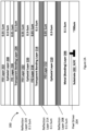
- FIG. 1 is a cross-sectional view of a single pixel tri-color coaxial LED device 100, in accordance with some embodiments.
- the tri-color coaxial LED device includes a substrate 102.
- the supporting substrate 102 is the substrate on which the array of individual driver circuits 104 is fabricated.
- the driver circuits could also be located in one of the layers above the substrate 102, or above the micro tri-color LED structure 100.
- Each driver circuit is a pixel driver 104.
- the pixel drivers are thin-film transistor pixel drivers or silicon CMOS pixel drivers.
- the substrate 102 is a Si substrate.
- the supporting substrate 102 is a transparent substrate, for example, a glass substrate.
- Other example substrates include GaAs, GaP, InP, SiC, ZnO, and sapphire substrates.
- the driver circuits 104 form individual pixel drivers to control the operation of the individual single pixel tri-color coaxial LED device 100.
- the circuitry on substrate 102 includes contacts to each individual pixel driver 104 and also a ground contact.
- Each micro tri-color LED structure 100 also has two types of contacts: P electrodes or anodes, such as 120, which are connected to the pixel driver; and N electrodes or cathodes, such as 122, 124, and 126, which are connected to the ground (i.e., the common electrode).
- a “structure” can take the form of a "layer”.
- three LED structures including three epitaxial layers 108, 112, and 116 are formed in a stacked structure, for example, the green LED epitaxial layer 112 is directly on top of the red LED epitaxial layer 108, and the blue LED epitaxial layer 112 is directly on top of the green epitaxial layer 112.
- the light emitted from the red epitaxial layer 108 is able to propagate through the green epitaxial layer 112 and then through the blue epitaxial layer 116 to be emitted out of the tri-color LED device 100.
- the light emitted from the green epitaxial layer 112 is able to propagate through the blue epitaxial layer 116 to be emitted out of the tri-color LED device 100.
- an LED structure includes many epitaxial sub-layers with different compositions.
- the LED epitaxial structures include III-V nitride, III-V arsenide, III-V phosphide, and III-V antimonide epitaxial structures.
- micro LEDs include GaN based UV/blue/green micro LEDs, AlInGaP based red/orange micro LEDs, and GaAs or InP based infrared (IR) micro LEDs.
- each of the stacked LED structures can be controlled individually to generate its individual light.
- the combined light from the top LED epitaxial layer as a result from the operations all the LED epitaxial layers in the tri-color coaxial LED device 100 can change the color of the single pixel on a display panel within a small footprint.
- the emitted colors of the LED structures included in the same device are not limited to red, green and blue.
- suitable colors can be selected from a range of different colors from a wavelength of 380 nm to 700 nm in visible color range.
- LED structures emitting other colors from invisible range such as ultra-violet and infrared can be implemented.
- the three-color choice, from bottom to top can be red, green, and blue.
- the three-color choice, from bottom to top can be ultra-violet, orange, and infrared.
- the wavelength of the light from the LED structure on one layer of the device 100 has to be longer than the wavelength from the LED structure on a layer on top of the current layer.
- the wavelength of the light from the bottom epitaxial layer 108 is longer than that of the middle epitaxial layer 112, and the wavelength of the light from the middle epitaxial layer 112 is longer than that of the top epitaxial layer 116.
- the wavelength of the light from the LED structure on one layer of the device 100 has to be shorter than the wavelength from the LED structure on a layer on top of the current layer.
- the wavelength of the light from the bottom epitaxial layer 108 is shorter than that of the middle epitaxial layer 112, and the wavelength of the light from the middle epitaxial layer 112 is shorter than that of the top epitaxial layer 116.
- an insulation layer 128 covers the top and side walls of the tri-color LED structures.
- a P-electrode 120 is placed on a side of the tri-color LED device 100 to connect to the red LED, green LED and blue LED structures.
- separate N-electrodes are placed to connect to each of the red LED, green LED, and blue LED structures.
- N-electrode 126 is connected to the red LED structure including the LED epitaxial layer 108.
- N-electrode 124 is connected to the green LED structure including the LED epitaxial layer 112.
- N-electrode 122 is connected to the blue LED structure including the LED epitaxial layer 116.
- the bottom epitaxial layer 108 is bonded to the substrate through a metal bonding layer 106.
- the metal bonding layer 106 can also be used as a reflector to reflect light emitted from the LED structures above.
- the middle epitaxial layer 112 is bonded to the bottom epitaxial layer 108 through a first transparent bonding layer 110.
- the top epitaxial layer 116 is bonded to the middle epitaxial layer 112 through a second transparent bonding layer 114.
- the transparent bonding layers can facilitate the light emitted from the layers below the bonding layers to pass through.
- reflection layers are formed between the LED epitaxial layers to improve light emission efficiency, which will be further described below.
- conductive transparent layers are formed between the LED epitaxial layers to improve conductivity and transparency.
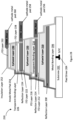
- Figure 2A is a cross-sectional view of a multiple layer structure 200 for forming the tri-color coaxial LED device, in accordance with some embodiments. More specifically, Figure 2A illustrates fabrication of the multiple layers on a substrate for the tri-color coaxial LED device.
- Figure 2A shows the substrate 202 supporting the pixel driver 204.
- the substrate 202 consists of Silicon and is around 700 microns thick.
- a metal (bonding) layer 206 is grown on the substrate 202.
- the metal (bonding) layer 206 may include ohmic contact layers, and metal bonding layers.
- the thickness of the metal (bonding) layer 206 is about 0.1 micron to about 3 microns.
- two metal layers are included in the metal (bonding) layer 206.
- One of the metal layers is deposited on an epitaxial layer 210, or on a reflection layer 208, which is immediately above the metal (bonding) layer 206.
- compositions for the metal (bonding) layer 206 include Au-Au bonding, Au-Sn bonding, Au-In bonding, Ti-Ti bonding, Cu-Cu bonding, or a mixture thereof.
- Au-Au bonding the two layers of Au respectively need a Cr coating as an adhesive layer, and Pt coating as an anti-diffusion layer. And the Pt coating is between the Au layer and the Cr layer. The Cr and Pt layers are positioned on the top and bottom of the two bonded Au layers.
- the mutual diffusion of Au on both layers bonds the two layers together.
- Eutectic bonding, thermal compression bonding, and transient liquid phase (TLP) bonding are example techniques that may be used.
- the epitaxial layer 210 is bonded on top of the existing structure of substrate 202 with the pixel driver 204 through the metal (bonding) layer 206.
- the epitaxial layer 210 is grown on a separate substrate (referred to as the epitaxy substrate). The epitaxy substrate is then removed after bonding, for example, by a laser lift-off process or wet chemical etching, leaving the structure shown in Figure 2A .
- the reflection layer 208 is coated on the epitaxial layer 210 before bonding.
- the reflection layer 208 is between the metal (bonding) layer 206 and the epitaxial layer 210 after bonding.
- the thickness of the reflection layer 208 is about 0.1 micron to about 5 microns.
- the reflection layer 208 includes a distributed Bragg reflector (DBR) structure.
- DBR distributed Bragg reflector
- the reflection layer 208 is formed from multiple layers of alternating or different materials with varying refractive index. In some instances, each layer boundary of the DBR structure causes a partial reflection of an optical wave.
- the reflection layer 208 can be used to reflect some selected wavelengths, for example, red light.
- the reflection layer 208 is made of multiple layers of SiO2 and Ti3O5. By varying the thicknesses and numbers of layers of SiO2 and Ti305 respectively, selective reflection or transmission of light at different wavelengths can be formed.
- the reflection layer 208 for a red light LED includes multiple layers of Au or/and Indium Tin Oxide (ITO).
- the reflection layer 208 for a red light LED structure has a low absorbance (for example, equal or less than 5%) of the light generated by different layers of the tri-color LED device. In some embodiments, the reflection layer 208 for a red light LED structure has a high reflectance (for example, equal or more than 95%) of the light generated above the current reflection layer, for example, the red light, the green light and the blue light.
- the epitaxial layer 210 is for forming red micro LEDs.
- a red LED epitaxial structure include III-V nitride, III-V arsenide, III-V phosphide, and III-V antimonide epitaxial structures.
- films within the red LED epitaxial layer 210 can include the layers of P-type GaP/P-type AlGaInP light-emitting layer/AlGaInP/N-type AlGaInP/N-type GaAs.
- P type is generally Mg-doped
- N-type is generally Si-doped.
- the thickness of the epitaxial layer 210 is about 0.3 micron to about 5 microns.
- ITO Indium Tin Oxide
- the thickness of the ITO layer 212 is about 0.01 micron to about 1 micron.
- the ITO layer 212 is deposited on the epitaxial layer 210 commonly by vapor deposition, for example, electron beam evaporation or sputtering deposition.
- ITO layers are used to maintain a good conductivity for electrode connection while in some instances, improving optical properties of the LED devices, such as reflectivity or transparency.
- a second reflection layer 214 is coated on the ITO layer 212 before any bonding process with the next epitaxial layer.
- the thickness of the reflection layer 214 is about 0.1 micron to about 5 microns.
- the reflection layer 214 includes a DBR structure.
- the reflection layer 214 is formed from multiple layers of alternating or different materials with varying refractive index.
- each layer boundary of the DBR structure causes a partial reflection of an optical wave.
- the reflection layer 214 can be used to reflect some selected wavelengths, for example, green light.
- the reflection layer 214 is made of multiple layers of SiO2 and Ti3O5. By varying the thicknesses and numbers of layers of SiO2 and Ti305 respectively, selective reflection or transmission of light at different wavelengths can be formed.
- the following DBR structure shown in table 1 is used to reflect green light from a green light LED:
- Table 1 DBR layer structure for a green light LED reflection layer.
- Layer composition Layer thickness (in nanometer) SiO2 1000 TiO2 109.54 SiO2 318.48 TiO2 64.95 SiO2 106.07 TiO2 245.76 SiO2 137.08 TiO2 65.14 SiO2 106.77 TiO2 338.95 SiO2 37.27 TiO2 12.41 SiO2 352.18 TiO2 70.83 SiO2 229.25 ITO 20
- the reflection layer 214 for a green light LED structure has a low absorbance (for example, equal or less than 5%) of the light generated by different layers of the tri-color LED device. In some embodiments, the reflection layer 214 for a green light LED structure has a high reflectance (for example, equal or more than 95%) of the light generated above the current reflection layer, for example, the green light and the blue light.
- a second epitaxial layer 220 is bonded on top of the first epitaxial layer 210 through the transparent bonding layer 216.
- the second epitaxial layer 220 is grown on a separate substrate (referred to as the epitaxy substrate).
- the epitaxy substrate is then removed after bonding, for example, by a laser lift-off process or wet chemical etching, leaving the structure shown in Figure 2A .
- the transparent bonding layer 216 is made of transparent plastic (resin) or SiO2, such as spin-on glass (SOG), bonding adhesive Micro Resist BCL-1200, etc.
- the thickness of the transparent bonding layer 216 is about 0.1 micron to about 5 microns.
- the second epitaxial layer 220 is for forming green micro LEDs.
- a green LED epitaxial structure include III-V nitride, III-V arsenide, III-V phosphide, and III-V antimonide epitaxial structures.
- films within the green LED epitaxial layer 220 can include the layers of P-type GaN/InGaN light-emitting layer/N-type GaN.
- P type is generally Mg-doped
- N-type is generally Si-doped.
- the thickness of the second epitaxial layer 220 is about 0.3 micron to about 5 microns.
- an ITO layer 218 is deposited on the second epitaxial layer 220 before bonding.
- the ITO layer 218 is between the transparent bonding layer 216 and the second epitaxial layer 220 after bonding.
- the thickness of the ITO layer 218 is about 0.01 micron to about 1 micron.
- another ITO layer 222 is deposited on top of the second epitaxial layer 220 before any bonding process with the next epitaxial layer.
- the thickness of the ITO layer 218 is about 0.01 micron to about 1 micron.
- a third reflection layer 224 is coated on the ITO layer 222 before any bonding process with the next epitaxial layer.
- the thickness of the reflection layer 224 is about 0.1 micron to about 5 microns.
- the reflection layer 224 includes a DBR structure.
- the reflection layer 224 is formed from multiple layers of alternating or different materials with varying refractive index.
- each layer boundary of the DBR structure causes a partial reflection of an optical wave.
- the reflection layer 224 can be used to reflect some selected wavelengths, for example, blue light.
- the reflection layer 224 is made of multiple layers of SiO2 and Ti3O5. By varying the thicknesses and numbers of layers of SiO2 and Ti3O5 respectively, selective reflection or transmission of light at different wavelengths can be formed.
- the following DBR structure shown in table 2 is used to reflect blue light from a blue light LED:
- Table 2 DBR layer structure for a blue light LED reflection layer.
- Layer composition Layer thickness (in nanometer) SiO2 1000 SiO2 183.36 TiO2 96 SiO2 84.65 TiO2 51.37 SiO2 332.37 TiO2 79.95 SiO2 423.13 TiO2 52.99 SiO2 35.87 TiO2 235.03 SiO2 253.67 TiO2 64.38 SiO2 336.08 ITO 20
- the reflection layer 224 for a blue light LED structure has a low absorbance (for example, equal or less than 5%) of the light generated by different layers of the tri-color LED device. In some embodiments, the reflection layer 224 for a blue light LED structure has a high reflectance (for example, equal or more than 95%) of the light generated above the current reflection layer, for example, the blue light.
- a third epitaxial layer 230 is bonded on top of the second epitaxial layer 220 through the transparent bonding layer 226.
- the third epitaxial layer 230 is grown on a separate substrate (referred to as the epitaxy substrate).
- the epitaxy substrate is then removed after bonding, for example, by a laser lift-off process or wet chemical etching, leaving the structure shown in Figure 2A .
- the transparent bonding layer 226 is made of transparent plastic (resin) or SiO2, such as spin-on glass (SOG), bonding adhesive Micro Resist BCL-1200, etc.
- the thickness of the transparent bonding layer 226 is about 0.1 micron to about 5 microns.
- the third epitaxial layer 230 is for forming blue micro LEDs.
- a blue LED epitaxial structure include III-V nitride, III-V arsenide, III-V phosphide, and III-V antimonide epitaxial structures.
- films within the blue LED epitaxial layer 230 can include the layers of P-type GaN/InGaN light-emitting layer/N-type GaN.
- P type is generally Mg-doped
- N-type is generally Si-doped.
- the thickness of the third epitaxial layer 230 is about 0.3 micron to about 5 microns.
- an ITO layer 228 is deposited on the third epitaxial layer 230 before bonding.
- the ITO layer 228 is between the transparent bonding layer 226 and the third epitaxial layer 230 after bonding.
- the thickness of the ITO layer 228 is about 0.01 micron to about 1 micron.
- another ITO layer 232 is deposited on top of the third epitaxial layer 230. In some embodiments, the thickness of the ITO layer 232 is about 0.01 micron to about 1 micron.
- Figure 2B is a cross-sectional view of a tri-color coaxial LED device 250 after the fabrication process, in accordance with some embodiments. More specifically, Figure 2B further illustrates the tri-color coaxial LED device 250 after some additional fabrication processes especially patterning of the multiple layer structure 200.
- a tri-color LED structure is formed and the axes of LED structures of different colors are aligned with one another vertically.
- the LED structures of different colors share the same axis.
- the LED structures of different colors form a pyramid like shape or a trapezoidal cross-sectional shape, with the lateral dimension of the bottom LED structure being the longest and the lateral dimension of the top LED structure being the shortest.
- Each layer has a narrower width or smaller area compared to a layer beneath it. In this instance, the width or area is measured by the dimensions of a plane parallel to the surface of the substrate 202.
- the bottom layer such as the metal (bonding) layer 206 has lateral dimension of about 1 micron to about 500 microns.
- a pyramid like shape will improve the electronic connections between the individual LED structures and to the electrodes, and simplify the fabrication process. For example, the electrode connections are exposed in each layer for easy connection.
- the aspect ratio of a cross section of a layer of the tri-color LED device remains substantially the same when the lateral dimension of the same layer varies. For example, when the lateral dimension of a patterned epitaxial layer is 5 microns, the thickness of the patterned epitaxial layer is less than a micron. In another example, when the lateral dimension of the same patterned epitaxial layer increases, the thickness of the same patterned epitaxial layer increases accordingly to maintain the same aspect ratio. In some embodiments, the aspect ratio of the cross-section of the epitaxial layers and other layers is less than 1/5 in thickness/width.
- the shape of the LED device is not limited and in some other embodiments, the cross-sectional shape of the tri-color coaxial LED device can take the form of other shapes, for example, a reverse trapezoid, a semi-oval, a rectangle, a parallelogram, a triangle, or a hexagon, etc.
- the top ITO layer 232 above the third epitaxial layer 230 is patterned using photolithography and etching.
- the etching method used to form the pattern is dry etching, for example, inductively coupled plasma (ICP) etching, or wet etching with an ITO etching solution.
- ICP inductively coupled plasma
- the same patterning methods can apply to all the other ITO layers, including ITO layers 212, 218, 222, 228 within the structure 200.
- the blue LED epitaxial layer 230 and the green LED epitaxial layer 220 are patterned using photolithography and etching.
- the etching method used to form the pattern is dry etching, for example, inductively coupled plasma (ICP) etching, with Cl2 and BCl3 etching gases.
- ICP inductively coupled plasma
- the transparent bonding layers including 216 and 226 are patterned using photolithography and etching.
- the etching method used to form the pattern is dry etching, for example, inductively coupled plasma (ICP) etching, with CF4 and O2 etching gases.
- ICP inductively coupled plasma
- the reflection layers including 208, 214 and 224 are patterned using photolithography and etching.
- the etching method used to form the pattern for the reflection layers especially the DBR layers is dry etching, for example, inductively coupled plasma (ICP) etching, with CF4 and O2 etching gases, or ion beam etching (IBE) with Ar gas.
- the red LED epitaxial layer 210 is patterned using photolithography and etching.
- the etching method used to form the pattern is dry etching, for example, inductively coupled plasma (ICP) etching, with Cl2 and HBr etching gases.
- ICP inductively coupled plasma
- the metal (bonding) layer 206 is patterned using photolithography and etching.
- the etching method used to form the pattern is dry etching, for example, inductively coupled plasma (ICP) etching, with Cl2/BCl3/Ar etching gases, or ion beam etching (IBE) with Ar gas.
- an insulation layer 252 is deposited on the surface of the patterned LED device structure including all the patterned layers, side walls, and the exposed substrate.
- the insulation layer 252 is made of SiO2 and/or Si3N4.
- the insulation layer 252 is made of TiO2.
- the insulation layer 252 is formed with composition similar to SiO2 after curing a layer such as SOG at a high temperature.
- the insulation layer 252 is made of a material that has a similar thermal coefficient of the layers underneath the insulation layer 252.
- the insulation layer 252 is patterned to expose the electrode contact area using photolithography and etching.
- the etching method used to form the pattern is dry etching, for example, inductively coupled plasma (ICP) etching, with CF4 and 02.
- anode metal pad 254 is vapor deposited on a suitable location of the patterned LED structure, such as on one side, to cover the red LED structure, the green LED structure, and the blue LED structure. In some embodiments, anode metal pad 254 is made to connect to the bottom metal (bonding) layer 206 of the red LED epitaxial layer 210, the bottom conductive ITO layer 218 of the green LED epitaxial layer 220, and the bottom conductive ITO layer 228 of the blue LED epitaxial layer 230. The anode metal pad 254 is also electrically connected to the integrated circuits including the pixel driver 204 on the substrate 202 through the metal (bonding) layer 206.
- cathode metal pad 256 is vapor deposited on a side of the patterned LED structure to connect to the red LED epitaxial layer 210 through the conductive ITO layer 212 on top of the red LED epitaxial layer 210.
- cathode metal pad 258 is vapor deposited on a side of the patterned LED structure to connect to the green LED epitaxial layer 220 through the conductive ITO layer 222 on top of the green LED epitaxial layer 220.
- cathode metal pad 260 is vapor deposited on a side of the patterned LED structure to connect to the blue LED epitaxial layer 230 through the conductive ITO layer 232 on top of the blue LED epitaxial layer 230.
- the external quantum efficiency for the red LED structure within the tri-color LED device is about 0.5-5%. In some embodiments, the external quantum efficiency for the green LED structure within the tri-color LED device is about 2-10%. In some embodiments, the external quantum efficiency for the blue LED structure within the tri-color LED device is about 5-15%. In some embodiments, the external quantum efficiency of the LED structure for each color is measured when the effects of all the related layers in addition to the LED structure such as reflection layers, bonding layers, ITO layers, and insulation layers are counted.
- the external quantum efficiency for the tri-color LED device 250 is about 20% or above. In some embodiments, the external quantum efficiency of the multi-color LED device is measured when the effects of all the layers in addition to the LED structure layers such as reflection layers, bonding layers, ITO layers, and insulation layers are counted.
- Various design aspects of the tri-color coaxial LED system 250 such as the dimensions of the layers (e.g., width, length, height, and cross-sectional area of each layer), the dimension of the electrodes, size, shape, spacing, and arrangement of the two or more LED structure layers, bonding layers, reflection layers and the conductive layers, and the configuration between the integrated circuits, pixel driver and electrical connections are selected (e.g., optimized using a cost or performance function) for obtaining the desired LED characteristics.
- LED characteristics that vary based on the above design aspects include, e.g., size, materials, cost, fabrication efficiency, light emission efficiency, power consumption, directivity, luminous intensity, luminous flux, color, spectrum and spatial radiation pattern.
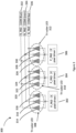
- Figure 3 is a circuit diagram illustrating a matrix of tri-color LED devices 300, in accordance with some embodiments.
- the circuit in Figure 3 includes three pixel drivers 302, 304, and 306 and three tri-color coaxial LED devices 308, 310, and 312.
- a display panel includes a plurality of pixels, such as millions of pixels, and each pixel includes a tri-color LED device structure.
- the LED device structures can be micro LEDs. Micro LEDs typically have a lateral dimension of 50 microns (um) or less, and can have lateral dimensions less than 10 um and even just a few um.
- the pixel driver for example 302, includes a number of transistors and capacitors (not shown in Figure 3 ).
- the transistors include a driving transistor connected to a voltage supply, and a control transistor configured with its gate connected to a scan signal bus line.
- the capacitors include a storage capacitor used maintain the gate voltage of the driving transistor during the time that the scan signal is setting other pixels.
- each of the three tri-color LED devices for example 308, have its own integrated circuit (IC) pixel driver 302.
- the tri-color LED device 308 for a single pixel can be viewed as three individual LEDs with different colors connected in parallel.
- the red LED 318, green LED 316, and blue LED 314, within the same tri-color LED device 308, are connected to the same IC pixel driver 302 via a shared P-electrode pad or anode, such as metal pad 254 in Figure 2B .
- each of the red, green, and blue LEDs within the same tri-color LED device 308 is connected to separate N-electrode pad or cathode.
- the red LED is connected to the N-electrode 336, such as metal pad 256 in Figure 2B .
- the green LED is connected to the N-electrode 334, such as metal pad 258 in Figure 2B .
- the blue LED is connected to the N-electrode 332, such as metal pad 260 in Figure 2B .
- all the red LEDs for example, 318, 324 and 330, from different tri-color LED devices, are connected to the same common N-electrode 336.
- All the green LEDs for example, 316, 322 and 328, from different tri-color LED devices, are connected to the same common N-electrode 334.
- the use of the common electrodes simplifies the fabrication process and reduces the area of the LED devices especially the footprint of the electrodes.
- Figure 4 is a flow diagram showing a method of fabricating a tri-color coaxial LED device 400, in accordance with some embodiments.
- Operations (e.g., steps) of the method 400 may be performed corresponding to embodiments described in Figures 1 , 2A , 2B and 3 above.
- the method 400 includes a step 402 of providing a substrate.
- a pixel driver is formed in the substrate.
- the method 400 also includes a step 404 of fabricating a first LED structure layer stacked on top of the substrate.
- the first LED structure layer includes a first epitaxial structure.
- the first LED structure layer is bonded on the substrate by a first bonding layer.
- a first reflection layer is coated on the first LED structure layer at the side facing the substrate before the bonding of the substrate and the first LED structure layer. And in some instances, the first reflection layer is between the first bonding layer and the first epitaxial structure after bonding.
- the first bonding layer is a conductive layer at the bottom of the first LED structure layer, and the first bonding layer is electrically connected to both the pixel driver and the bottom of the first LED structure layer.
- a first upper conductive layer is coated at the top of the first LED structure layer to electrically connect to the top of the first LED structure layer and a common electrode.
- the method 400 further includes a step 406 of fabricating a second LED structure layer stacked on top of the first LED structure layer.
- the second LED structure layer includes a second epitaxial structure.
- the second LED structure is bonded on the first LED structure by a second bonding layer.
- a second reflection layer is coated on the first LED structure layer at the side facing the second LED structure layer before the bonding of the first LED structure layer and the second LED structure layer. And in some instances, the second reflection layer is between the first upper conductive layer and the second bonding layer after bonding.
- a second lower conductive layer is coated at the bottom of the second LED structure layer, and the second lower conductive layer is electrically connected to both the pixel driver and the bottom of the second LED structure layer.
- a second upper conductive layer is coated at the top of the second LED structure layer to electrically connect to the top of the second LED structure layer and a common electrode.
- the method 400 further includes a step 408 of fabricating a third LED structure layer stacked on top of the second LED structure layer.
- the third LED structure layer includes a third epitaxial structure.
- the third LED structure is bonded on the second LED structure by a third bonding layer.
- a third reflection layer is coated on the second LED structure layer at the side facing the third LED structure layer before the bonding of the second LED structure layer and the third LED structure layer. And in some instances, the third reflection layer is between the second upper conductive layer and the third bonding layer after bonding.
- a third lower conductive layer is coated at the bottom of the third LED structure layer, and the third lower conductive layer is electrically connected to both the pixel driver and the bottom of the third LED structure layer.
- a third upper conductive layer is coated at the top of the third LED structure layer to electrically connect to the top of the third LED structure layer and a common electrode.
- the first LED structure layer, the second LED structure layer, and the third LED structure layer substantially overlap laterally with one another to form a light path that combines light emitted from the first LED structure layer, the second LED structure layer and the third LED structure layer.
- the method 400 further includes a step 410 of patterning each of the layers formed from steps 402-408 described above by photolithography and etching to form three LEDs directly stacked together.
- the method 400 further includes a step 412 of depositing an insulation layer above the exposed structures formed from steps 402-410 described above and etching the insulation layer for coating the electrode contact pads.
- the methods 400 further includes a step of 414 of coating the electrode contact pads on the surface of the structures formed from steps 402-412.
- an anode metal contact pad is coated to electrically connect to the lower conductive layer of each of the first, second and third LED structure layers, and the pixel drive.
- a first cathode metal contact pad is coated to electrically connect to the upper conductive layer of the first LED structure layer.
- a second cathode metal contact pad is coated to electrically connect to the upper conductive layer of the second LED structure layer.
- a third cathode metal contact pad is coated to electrically connect to the upper conductive layer of the third LED structure layer.
- FIG. 1 Further embodiments also include various subsets of the above embodiments including embodiments in Figures 1 , 2A , 2B , 3 , and 4 combined or otherwise re-arranged in various embodiments.
- FIG. 5 is a top view of a micro LED display panel 500, in accordance with some embodiments.
- the display panel 500 includes a data interface 510, a control module 520 and a pixel region 550.
- the data interface 510 receives data defining the image to be displayed. The source(s) and format of this data will vary depending on the application.
- the control module 520 receives the incoming data and converts it to a form suitable to drive the pixels in the display panel.
- the control module 520 may include digital logic and/or state machines to convert from the received format to one appropriate for the pixel region 550, shift registers or other types of buffers and memory to store and transfer the data, digital-to-analog converters and level shifters, and scan controllers including clocking circuitry.
- the pixel region 550 includes an array of pixels.
- the pixels include micro LEDs, such as a tri-color coaxial LED 534, integrated with pixel drivers, for example as described above.
- the display panel 500 is a color RGB display panel. It includes red, green and blue pixels.
- the tri-color coaxial LED 534 is controlled by a pixel driver.
- the pixel makes contact to a supply voltage (not shown) and ground via a ground pad 536, and also to a control signal, according to the embodiments shown previously.
- the p-electrode of the tri-color coaxial LED 534 and the output of the driving transistor are positioned within the LED 534, and they are electrically connected by the bonding metal layer, such as the metal layer 204 in Figure 2A .
- the LED current driving signal connection between p-electrode of LED and output of the pixel driver
- ground connection between n-electrode and system ground
- the supply voltage Vdd connection between source of the pixel driver and system Vdd
- the control signal connection to the gate of the pixel driver are made in accordance with various embodiments.
- Figure 5 is merely a representative figure. Other designs will be apparent. For example, the colors do not have to be red, green and blue. They also do not have to be arranged in columns or stripes. As one example, apart from the arrangement of a square matrix of pixels shown in Figure 5 , an arrangement of hexagonal matrix of pixels can also be used to form the display panel 500.
- a fully programmable rectangular array of pixels is not necessary.
- Other designs of display panels with a variety of shapes and displays may also be formed using the device structures described herein.
- One class of examples is specialty applications, including signage and automotive. For example, multiple pixels may be arranged in the shape of a star or a spiral to form a display panel, and different patterns on the display panel can be produced by turning on and off the LEDs.
- Another specialty example is automobile headlights and smart lighting, where certain pixels are grouped together to form various illumination shapes and each group of LED pixels can be turned on or off or otherwise adjusted by individual pixel drivers.
- each LED is located on top of the corresponding pixel driver circuit.
- the pixel drivers could also be located “behind”, “in front of”, or “beside” the LED.
- the resolution of a display panel can range typically from 8x8 to 3840x2160.
- Common display resolutions include QVGA with 320x240 resolution and an aspect ratio of 4:3, XGA with 1024x768 resolution and an aspect ratio of 4:3, D with 1280x720 resolution and an aspect ratio of 16:9, FHD with 1920x1080 resolution and an aspect ratio of 16:9, UHD with 3840x2160 resolution and an aspect ratio of 16:9, and 4K with 4096x2160 resolution.
- the size of the overall display region can also vary widely, ranging from diagonals as small as tens of microns or less up to hundreds of inches or more.
- Example applications include direct viewing display screens, light engines for home/office projectors and portable electronics such as smart phones, laptops, wearable electronics, AR and VR glasses, and retinal projections.
- the power consumption can vary from as low as a few milliwatts for retinal projectors to as high as kilowatts for large screen outdoor displays, projectors, and smart automobile headlights.
- frame rate due to the fast response (nanoseconds) of inorganic LEDs, the frame rate can be as high as KHz, or even MHz for small resolutions.
- FIG. 1 Further embodiments also include various subsets of the above embodiments including embodiments in Figures 1 , 2A , 2B , and 3-5 combined or otherwise re-arranged in various embodiments.
- non-LED devices include vertical cavity surface emitting lasers (VCSEL), photodetectors, micro-electro-mechanical system (MEMS), silicon photonic devices, power electronic devices, and distributed feedback lasers (DFB).
- VCSEL vertical cavity surface emitting lasers
- MEMS micro-electro-mechanical system
- DFB distributed feedback lasers
- control circuitry include current drivers, voltage drivers, trans-impedance amplifiers, and logic circuits.
- the storage medium can include, but is not limited to, high-speed random access memory, such as DRAM, SRAM, DDR RAM or other random access solid state memory devices, and may include non-volatile memory, such as one or more magnetic disk storage devices, optical disk storage devices, flash memory devices, or other non-volatile solid state storage devices.
- Memory optionally includes one or more storage devices remotely located from the CPU(s). Memory or alternatively the non-volatile memory device(s) within the memory, comprises a non-transitory computer readable storage medium.
- features of the present invention can be incorporated in software and/or firmware for controlling the hardware of a processing system, and for enabling a processing system to interact with other mechanisms utilizing the results of the present invention.
- software or firmware may include, but is not limited to, application code, device drivers, operating systems, and execution environments/containers.
- the term “if” may be construed to mean “when” or “upon” or “in response to determining” or “in accordance with a determination” or “in response to detecting,” that a stated condition precedent is true, depending on the context.
- the phrase “if it is determined [that a stated condition precedent is true]” or “if [a stated condition precedent is true]” or “when [a stated condition precedent is true]” may be construed to mean “upon determining” or “in response to determining” or “in accordance with a determination” or “upon detecting” or “in response to detecting” that the stated condition precedent is true, depending on the context.
- Preferred embodiments of the invention are defined in the following paras 1 to 41:
Landscapes
- Led Devices (AREA)
- Devices For Indicating Variable Information By Combining Individual Elements (AREA)
- Led Device Packages (AREA)
- Transforming Electric Information Into Light Information (AREA)
Priority Applications (1)
| Application Number | Priority Date | Filing Date | Title |
|---|---|---|---|
| DE24203353.8T DE24203353T1 (de) | 2019-06-19 | 2020-06-18 | Systeme und verfahren für koaxiale mehrfarbige led |
Applications Claiming Priority (3)
| Application Number | Priority Date | Filing Date | Title |
|---|---|---|---|
| US201962863559P | 2019-06-19 | 2019-06-19 | |
| EP20825423.5A EP3987580A4 (de) | 2019-06-19 | 2020-06-18 | Systeme und verfahren für koaxiale mehrfarbige led |
| PCT/US2020/038337 WO2020257391A1 (en) | 2019-06-19 | 2020-06-18 | Systems and methods for coaxial multi-color led |
Related Parent Applications (1)
| Application Number | Title | Priority Date | Filing Date |
|---|---|---|---|
| EP20825423.5A Division EP3987580A4 (de) | 2019-06-19 | 2020-06-18 | Systeme und verfahren für koaxiale mehrfarbige led |
Publications (2)
| Publication Number | Publication Date |
|---|---|
| EP4465355A2 true EP4465355A2 (de) | 2024-11-20 |
| EP4465355A3 EP4465355A3 (de) | 2025-03-19 |
Family
ID=74038681
Family Applications (4)
| Application Number | Title | Priority Date | Filing Date |
|---|---|---|---|
| EP24203353.8A Withdrawn EP4465355A3 (de) | 2019-06-19 | 2020-06-18 | Systeme und verfahren für koaxiale mehrfarbige led |
| EP24206108.3A Withdrawn EP4468350A3 (de) | 2019-06-19 | 2020-06-18 | Systeme und verfahren für koaxiale mehrfarbige led |
| EP20825423.5A Withdrawn EP3987580A4 (de) | 2019-06-19 | 2020-06-18 | Systeme und verfahren für koaxiale mehrfarbige led |
| EP24206106.7A Withdrawn EP4468349A3 (de) | 2019-06-19 | 2020-06-18 | Systeme und verfahren für koaxiale mehrfarbige led |
Family Applications After (3)
| Application Number | Title | Priority Date | Filing Date |
|---|---|---|---|
| EP24206108.3A Withdrawn EP4468350A3 (de) | 2019-06-19 | 2020-06-18 | Systeme und verfahren für koaxiale mehrfarbige led |
| EP20825423.5A Withdrawn EP3987580A4 (de) | 2019-06-19 | 2020-06-18 | Systeme und verfahren für koaxiale mehrfarbige led |
| EP24206106.7A Withdrawn EP4468349A3 (de) | 2019-06-19 | 2020-06-18 | Systeme und verfahren für koaxiale mehrfarbige led |
Country Status (7)
| Country | Link |
|---|---|
| US (4) | US11538850B2 (de) |
| EP (4) | EP4465355A3 (de) |
| JP (2) | JP7592035B2 (de) |
| KR (2) | KR20220024706A (de) |
| CN (2) | CN114793476A (de) |
| DE (3) | DE20825423T1 (de) |
| WO (1) | WO2020257391A1 (de) |
Families Citing this family (46)
| Publication number | Priority date | Publication date | Assignee | Title |
|---|---|---|---|---|
| WO2020257391A1 (en) * | 2019-06-19 | 2020-12-24 | Hong Kong Beida Jade Bird Display Limited | Systems and methods for coaxial multi-color led |
| US11658275B2 (en) * | 2019-10-28 | 2023-05-23 | Seoul Viosys Co., Ltd. | Light emitting device for display and LED display apparatus having the same |
| JP7709433B2 (ja) * | 2019-10-28 | 2025-07-16 | ソウル バイオシス カンパニー リミテッド | ディスプレイ用発光素子及びそれを有するledディスプレイ装置 |
| CN112035007B (zh) * | 2020-08-11 | 2022-02-22 | 惠州市华星光电技术有限公司 | 触控显示面板及其制备方法 |
| US11476299B2 (en) * | 2020-08-31 | 2022-10-18 | Hong Kong Beida Jade Bird Display Limited | Double color micro LED display panel |
| CN112786767B (zh) * | 2021-01-11 | 2022-04-22 | 南京大学 | 流体组装的微米级器件模组及其制造方法 |
| US20220285578A1 (en) * | 2021-03-08 | 2022-09-08 | Samsung Electronics Co., Ltd. | Light-emitting diode and display device including the same |
| JP7736073B2 (ja) * | 2021-09-03 | 2025-09-09 | ソニーグループ株式会社 | 発光デバイスおよび電子機器 |
| KR20240093642A (ko) * | 2021-11-16 | 2024-06-24 | 엘지전자 주식회사 | 디스플레이 장치 |
| KR102599275B1 (ko) * | 2022-01-25 | 2023-11-07 | 주식회사 썬다이오드코리아 | 수직 적층 구조를 가지는 마이크로 디스플레이의 화소 |
| CN114664983B (zh) * | 2022-03-22 | 2023-03-21 | 西湖大学 | 一种基于Micro LED的显示装置的制作方法以及显示装置 |
| CN114497112B (zh) * | 2022-03-30 | 2022-07-15 | 季华实验室 | 一种MicroLED显示面板制作方法及显示面板 |
| US12604563B2 (en) * | 2022-04-25 | 2026-04-14 | Seoul Viosys Co., Ltd. | Light emitting device and light emitting module having the same |
| CN117317090A (zh) * | 2022-06-22 | 2023-12-29 | 成都辰显光电有限公司 | 一种微型显示模组、显示面板及制备方法 |
| CN115050873B (zh) * | 2022-06-27 | 2026-01-02 | 厦门未来显示技术研究院有限公司 | 一种RGB Micro-LED芯片及其制作方法 |
| CN115332285B (zh) * | 2022-07-22 | 2025-06-27 | 中国电子科技集团公司第五十五研究所 | 一种多色Micro-LED显示器件的制作方法 |
| KR20250065679A (ko) * | 2022-09-09 | 2025-05-13 | 제이드 버드 디스플레이(상하이) 리미티드 | 발광 효율 향상용 발광 픽셀 구조 시스템 및 이의 제조방법 |
| CN115274945B (zh) * | 2022-09-30 | 2022-12-23 | 江西兆驰半导体有限公司 | 一种Micro-LED芯片封装方法 |
| KR102904191B1 (ko) * | 2022-10-05 | 2025-12-26 | 엘지전자 주식회사 | 디스플레이 화소용 적층형 반도체 발광소자 및 이를 포함하는 디스플레이 장치 |
| CN115810622A (zh) * | 2022-11-02 | 2023-03-17 | 上海芯元基半导体科技有限公司 | Led芯片及其制作方法、电子设备及其制作方法 |
| WO2024117311A1 (ko) * | 2022-11-30 | 2024-06-06 | 엘지전자 주식회사 | 디스플레이 화소용 적층형 반도체 발광소자 및 이를 포함하는 디스플레이 장치 |
| CN115881863B (zh) * | 2022-12-22 | 2023-10-13 | 北京大学东莞光电研究院 | 三色氮化物发光二极管的制造方法 |
| KR20250130189A (ko) * | 2022-12-23 | 2025-09-01 | 제이드 버드 디스플레이(상하이) 리미티드 | 마이크로 led 구조 및 마이크로 led 패널 |
| JP2025541629A (ja) * | 2022-12-23 | 2025-12-23 | ジェイド バード ディスプレイ(シャンハイ) リミテッド | マイクロled構造体およびフルカラーマイクロledパネル |
| JP2025539961A (ja) * | 2022-12-23 | 2025-12-11 | ジェイド バード ディスプレイ(シャンハイ) リミテッド | マイクロled構造体およびマイクロledパネル |
| KR20240108049A (ko) * | 2022-12-30 | 2024-07-09 | 엘지디스플레이 주식회사 | 표시장치 |
| KR20250171150A (ko) * | 2023-03-30 | 2025-12-08 | 제이드 버드 디스플레이(상하이) 리미티드 | 마이크로 led 구조 및 마이크로 led 패널 |
| US20240355791A1 (en) * | 2023-04-20 | 2024-10-24 | Seoul Viosys Co., Ltd. | Display module and display apparatus having light emitting device |
| WO2024229588A1 (en) * | 2023-05-05 | 2024-11-14 | Jade Bird Display (shanghai) Limited | Micro led display panel |
| DE112024002096T5 (de) * | 2023-05-16 | 2026-02-26 | Ams-Osram International Gmbh | Optoelektronische vorrichtung und system zur optischen datenübertragung |
| CN119181713B (zh) * | 2023-06-21 | 2025-09-23 | 武汉华星光电半导体显示技术有限公司 | 显示模组及显示装置 |
| WO2025010706A1 (en) * | 2023-07-13 | 2025-01-16 | Jade Bird Display (shanghai) Limited | Micro led and micro led display panel |
| WO2025015596A1 (zh) * | 2023-07-20 | 2025-01-23 | 京东方科技集团股份有限公司 | 显示面板及显示装置 |
| CN117334711A (zh) * | 2023-07-26 | 2024-01-02 | 上海显耀显示科技有限公司 | Micro led显示面板及制造方法 |
| CN119486396A (zh) * | 2023-07-31 | 2025-02-18 | 武汉华星光电半导体显示技术有限公司 | 显示背板及显示装置 |
| US20250079409A1 (en) * | 2023-09-05 | 2025-03-06 | Creeled, Inc. | Multiple junction light-emitting diode chips and related methods |
| CN119630158B (zh) * | 2023-09-12 | 2025-11-21 | 武汉华星光电半导体显示技术有限公司 | 显示面板及显示装置 |
| US20250105220A1 (en) * | 2023-09-27 | 2025-03-27 | Rayleigh Vision Limited | Vertically stacked light-emitting diode structure |
| CN119836093B (zh) * | 2023-10-11 | 2025-10-17 | 武汉华星光电半导体显示技术有限公司 | 一种显示装置 |
| CN119894309B (zh) * | 2023-10-24 | 2025-09-23 | 武汉华星光电半导体显示技术有限公司 | 显示面板及显示装置 |
| KR20250130871A (ko) | 2024-02-26 | 2025-09-02 | 한국전자기술연구원 | 픽셀용 멀티 칩 패키지, 그를 포함하는 표시 장치 및 그의 제조 방법 |
| CN118231547A (zh) * | 2024-05-06 | 2024-06-21 | 上海显耀显示科技有限公司 | 微型led显示芯片及其形成方法 |
| CN121730005A (zh) * | 2024-07-23 | 2026-03-24 | 京东方科技集团股份有限公司 | 显示面板及其制作方法、显示装置 |
| CN119546019A (zh) * | 2024-10-14 | 2025-02-28 | 上海大学 | 一种基于垂直堆叠的全彩Micro-LED微显示器件及其制备方法 |
| CN119364965B (zh) * | 2024-12-05 | 2025-10-31 | 武汉华星光电半导体显示技术有限公司 | 显示面板及显示装置 |
| CN119653957A (zh) * | 2025-02-18 | 2025-03-18 | 西湖烟山科技(杭州)有限公司 | 显示芯片及其制作方法 |
Family Cites Families (32)
| Publication number | Priority date | Publication date | Assignee | Title |
|---|---|---|---|---|
| JP3259931B2 (ja) * | 1992-04-17 | 2002-02-25 | シャープ株式会社 | 半導体発光素子および半導体表示装置 |
| JPH08274376A (ja) * | 1995-03-15 | 1996-10-18 | Texas Instr Inc <Ti> | シリコンに格子整合したiii−v化合物半導体エミッター |
| US6956701B1 (en) * | 2004-04-26 | 2005-10-18 | Infocus Corporation | Method and apparatus for combining light paths of multiple colored light sources through a common integration tunnel |
| US7393469B2 (en) | 2003-07-31 | 2008-07-01 | Ramazan Benrashid | High performance sol-gel spin-on glass materials |
| US20070170444A1 (en) | 2004-07-07 | 2007-07-26 | Cao Group, Inc. | Integrated LED Chip to Emit Multiple Colors and Method of Manufacturing the Same |
| WO2009010762A1 (en) | 2007-07-19 | 2009-01-22 | Photonstar Led Limited | Vertical led with conductive vias |
| TW201017863A (en) | 2008-10-03 | 2010-05-01 | Versitech Ltd | Semiconductor color-tunable broadband light sources and full-color microdisplays |
| TWI436458B (zh) | 2011-07-29 | 2014-05-01 | 鴻海精密工業股份有限公司 | 晶圓級封裝結構及其製作方法 |
| US9494294B2 (en) | 2012-03-23 | 2016-11-15 | Cree, Inc. | Modular indirect troffer |
| US9178123B2 (en) | 2012-12-10 | 2015-11-03 | LuxVue Technology Corporation | Light emitting device reflective bank structure |
| US9196606B2 (en) | 2013-01-09 | 2015-11-24 | Nthdegree Technologies Worldwide Inc. | Bonding transistor wafer to LED wafer to form active LED modules |
| US10304811B2 (en) * | 2015-09-04 | 2019-05-28 | Hong Kong Beida Jade Bird Display Limited | Light-emitting diode display panel with micro lens array |
| US10388691B2 (en) * | 2016-05-18 | 2019-08-20 | Globalfoundries Inc. | Light emitting diodes (LEDs) with stacked multi-color pixels for displays |
| US10037981B2 (en) | 2016-05-18 | 2018-07-31 | Globalfoundries Inc. | Integrated display system with multi-color light emitting diodes (LEDs) |
| US10304375B2 (en) | 2016-09-23 | 2019-05-28 | Hong Kong Beida Jade Bird Display Limited | Micro display panels with integrated micro-reflectors |
| US10412806B2 (en) | 2016-11-10 | 2019-09-10 | Hong Kong Beida Jade Bird Display Limited | Multi-color micro-LED array light source |
| US10325893B2 (en) | 2016-12-13 | 2019-06-18 | Hong Kong Beida Jade Bird Display Limited | Mass transfer of micro structures using adhesives |
| CN106876406B (zh) * | 2016-12-30 | 2023-08-08 | 上海君万微电子科技有限公司 | 基于iii-v族氮化物半导体的led全彩显示器件结构及制备方法 |
| CN110462850B (zh) * | 2017-03-20 | 2024-04-16 | 上海显耀显示科技有限公司 | 通过堆叠微型led的层来制造半导体器件 |
| US10733930B2 (en) * | 2017-08-23 | 2020-08-04 | Facebook Technologies, Llc | Interposer for multi-layer display architecture |
| TWI643328B (zh) | 2017-10-13 | 2018-12-01 | 英屬開曼群島商錼創科技股份有限公司 | 顯示裝置 |
| KR20190061227A (ko) * | 2017-11-27 | 2019-06-05 | 광주과학기술원 | 마이크로 led 장치 및 그 제조 방법 |
| US10892297B2 (en) * | 2017-11-27 | 2021-01-12 | Seoul Viosys Co., Ltd. | Light emitting diode (LED) stack for a display |
| US11282981B2 (en) | 2017-11-27 | 2022-03-22 | Seoul Viosys Co., Ltd. | Passivation covered light emitting unit stack |
| US12100696B2 (en) * | 2017-11-27 | 2024-09-24 | Seoul Viosys Co., Ltd. | Light emitting diode for display and display apparatus having the same |
| US11552057B2 (en) * | 2017-12-20 | 2023-01-10 | Seoul Viosys Co., Ltd. | LED unit for display and display apparatus having the same |
| US11114499B2 (en) | 2018-01-02 | 2021-09-07 | Seoul Viosys Co., Ltd. | Display device having light emitting stacked structure |
| US10325894B1 (en) * | 2018-04-17 | 2019-06-18 | Shaoher Pan | Integrated multi-color light-emitting pixel arrays based devices by bonding |
| TWI688933B (zh) | 2018-07-16 | 2020-03-21 | 友達光電股份有限公司 | 顯示裝置 |
| US11508876B2 (en) * | 2018-12-31 | 2022-11-22 | Seoul Viosys Co., Ltd. | Light emitting device package and display device having the same |
| US10790603B2 (en) | 2019-02-01 | 2020-09-29 | Intel Corporation | Connector with relaxation mechanism for latch |
| WO2020257391A1 (en) * | 2019-06-19 | 2020-12-24 | Hong Kong Beida Jade Bird Display Limited | Systems and methods for coaxial multi-color led |
-
2020
- 2020-06-18 WO PCT/US2020/038337 patent/WO2020257391A1/en not_active Ceased
- 2020-06-18 EP EP24203353.8A patent/EP4465355A3/de not_active Withdrawn
- 2020-06-18 DE DE20825423.5T patent/DE20825423T1/de active Pending
- 2020-06-18 KR KR1020227001828A patent/KR20220024706A/ko not_active Ceased
- 2020-06-18 US US16/904,841 patent/US11538850B2/en active Active
- 2020-06-18 EP EP24206108.3A patent/EP4468350A3/de not_active Withdrawn
- 2020-06-18 JP JP2021573780A patent/JP7592035B2/ja active Active
- 2020-06-18 EP EP20825423.5A patent/EP3987580A4/de not_active Withdrawn
- 2020-06-18 CN CN202080044771.4A patent/CN114793476A/zh active Pending
- 2020-06-18 EP EP24206106.7A patent/EP4468349A3/de not_active Withdrawn
- 2020-06-18 DE DE24203353.8T patent/DE24203353T1/de active Pending
- 2020-06-18 KR KR1020247032330A patent/KR20240149971A/ko active Pending
- 2020-06-18 DE DE24206108.3T patent/DE24206108T1/de active Pending
- 2020-06-18 CN CN202411093333.3A patent/CN119421567A/zh active Pending
-
2022
- 2022-11-17 US US17/989,624 patent/US11955505B2/en active Active
-
2024
- 2024-03-02 US US18/593,871 patent/US12402461B2/en active Active
- 2024-09-25 JP JP2024165882A patent/JP2025000754A/ja not_active Withdrawn
-
2025
- 2025-07-29 US US19/284,479 patent/US20250359406A1/en active Pending
Also Published As
| Publication number | Publication date |
|---|---|
| US12402461B2 (en) | 2025-08-26 |
| EP4468350A2 (de) | 2024-11-27 |
| US20230077969A1 (en) | 2023-03-16 |
| EP3987580A4 (de) | 2023-07-12 |
| JP7592035B2 (ja) | 2024-11-29 |
| EP4468349A2 (de) | 2024-11-27 |
| EP4465355A3 (de) | 2025-03-19 |
| CN119421567A (zh) | 2025-02-11 |
| JP2025000754A (ja) | 2025-01-07 |
| CN114793476A (zh) | 2022-07-26 |
| EP4468350A3 (de) | 2025-03-05 |
| US11538850B2 (en) | 2022-12-27 |
| JP2022537156A (ja) | 2022-08-24 |
| KR20240149971A (ko) | 2024-10-15 |
| EP4468349A3 (de) | 2025-03-05 |
| EP3987580A1 (de) | 2022-04-27 |
| KR20220024706A (ko) | 2022-03-03 |
| DE24206108T1 (de) | 2025-05-28 |
| US20240250111A1 (en) | 2024-07-25 |
| US11955505B2 (en) | 2024-04-09 |
| DE24203353T1 (de) | 2025-03-13 |
| WO2020257391A1 (en) | 2020-12-24 |
| DE20825423T1 (de) | 2023-11-09 |
| US20200403026A1 (en) | 2020-12-24 |
| US20250359406A1 (en) | 2025-11-20 |
Similar Documents
| Publication | Publication Date | Title |
|---|---|---|
| US12402461B2 (en) | Systems and methods for coaxial multi-color LED | |
| US20260005204A1 (en) | Systems and methods for led with stacked bonding structures | |
| TWI864208B (zh) | 用於同軸多色led之系統和方法 | |
| US12211970B2 (en) | Micro light emitting diode with high light extraction efficiency | |
| US20250006773A1 (en) | Systems and Methods for Coaxial Multi-Color LED | |
| HK40115804A (en) | Systems and methods for coaxial multi-color led | |
| HK40113312A (en) | Systems and methods for coaxial multi-color led | |
| HK40115556A (en) | Systems and methods for coaxial multi-color led | |
| TWI889574B (zh) | 用於同軸多色led之系統和方法 |
Legal Events
| Date | Code | Title | Description |
|---|---|---|---|
| PUAI | Public reference made under article 153(3) epc to a published international application that has entered the european phase |
Free format text: ORIGINAL CODE: 0009012 |
|
| STAA | Information on the status of an ep patent application or granted ep patent |
Free format text: STATUS: THE APPLICATION HAS BEEN PUBLISHED |
|
| AC | Divisional application: reference to earlier application |
Ref document number: 3987580 Country of ref document: EP Kind code of ref document: P |
|
| AK | Designated contracting states |
Kind code of ref document: A2 Designated state(s): AL AT BE BG CH CY CZ DE DK EE ES FI FR GB GR HR HU IE IS IT LI LT LU LV MC MK MT NL NO PL PT RO RS SE SI SK SM TR |
|
| P01 | Opt-out of the competence of the unified patent court (upc) registered |
Free format text: CASE NUMBER: APP_62050/2024 Effective date: 20241120 |
|
| PUAL | Search report despatched |
Free format text: ORIGINAL CODE: 0009013 |
|
| REG | Reference to a national code |
Ref country code: DE Ref legal event code: R210 |
|
| AK | Designated contracting states |
Kind code of ref document: A3 Designated state(s): AL AT BE BG CH CY CZ DE DK EE ES FI FR GB GR HR HU IE IS IT LI LT LU LV MC MK MT NL NO PL PT RO RS SE SI SK SM TR |
|
| RIC1 | Information provided on ipc code assigned before grant |
Ipc: H10H 29/39 20250101ALI20250210BHEP Ipc: H01L 25/16 20230101AFI20250210BHEP |
|
| REG | Reference to a national code |
Ref country code: HK Ref legal event code: DE Ref document number: 40115804 Country of ref document: HK |
|
| STAA | Information on the status of an ep patent application or granted ep patent |
Free format text: STATUS: THE APPLICATION HAS BEEN WITHDRAWN |
|
| 18W | Application withdrawn |
Effective date: 20250722 |