EP4477257A2 - Implantat - Google Patents
Implantat Download PDFInfo
- Publication number
- EP4477257A2 EP4477257A2 EP24209372.2A EP24209372A EP4477257A2 EP 4477257 A2 EP4477257 A2 EP 4477257A2 EP 24209372 A EP24209372 A EP 24209372A EP 4477257 A2 EP4477257 A2 EP 4477257A2
- Authority
- EP
- European Patent Office
- Prior art keywords
- electronic module
- energy storage
- storage device
- implant
- connection
- Prior art date
- Legal status (The legal status is an assumption and is not a legal conclusion. Google has not performed a legal analysis and makes no representation as to the accuracy of the status listed.)
- Pending
Links
Images







Classifications
-
- A—HUMAN NECESSITIES
- A61—MEDICAL OR VETERINARY SCIENCE; HYGIENE
- A61N—ELECTROTHERAPY; MAGNETOTHERAPY; RADIATION THERAPY; ULTRASOUND THERAPY
- A61N1/00—Electrotherapy; Circuits therefor
- A61N1/18—Applying electric currents by contact electrodes
- A61N1/32—Applying electric currents by contact electrodes alternating or intermittent currents
- A61N1/36—Applying electric currents by contact electrodes alternating or intermittent currents for stimulation
- A61N1/372—Arrangements in connection with the implantation of stimulators
- A61N1/375—Constructional arrangements, e.g. casings
-
- A—HUMAN NECESSITIES
- A61—MEDICAL OR VETERINARY SCIENCE; HYGIENE
- A61N—ELECTROTHERAPY; MAGNETOTHERAPY; RADIATION THERAPY; ULTRASOUND THERAPY
- A61N1/00—Electrotherapy; Circuits therefor
- A61N1/18—Applying electric currents by contact electrodes
- A61N1/32—Applying electric currents by contact electrodes alternating or intermittent currents
- A61N1/36—Applying electric currents by contact electrodes alternating or intermittent currents for stimulation
- A61N1/372—Arrangements in connection with the implantation of stimulators
- A61N1/375—Constructional arrangements, e.g. casings
- A61N1/3752—Details of casing-lead connections
- A61N1/3754—Feedthroughs
-
- A—HUMAN NECESSITIES
- A61—MEDICAL OR VETERINARY SCIENCE; HYGIENE
- A61N—ELECTROTHERAPY; MAGNETOTHERAPY; RADIATION THERAPY; ULTRASOUND THERAPY
- A61N1/00—Electrotherapy; Circuits therefor
- A61N1/18—Applying electric currents by contact electrodes
- A61N1/32—Applying electric currents by contact electrodes alternating or intermittent currents
- A61N1/36—Applying electric currents by contact electrodes alternating or intermittent currents for stimulation
- A61N1/372—Arrangements in connection with the implantation of stimulators
- A61N1/378—Electrical supply
-
- A—HUMAN NECESSITIES
- A61—MEDICAL OR VETERINARY SCIENCE; HYGIENE
- A61N—ELECTROTHERAPY; MAGNETOTHERAPY; RADIATION THERAPY; ULTRASOUND THERAPY
- A61N1/00—Electrotherapy; Circuits therefor
- A61N1/18—Applying electric currents by contact electrodes
- A61N1/32—Applying electric currents by contact electrodes alternating or intermittent currents
- A61N1/36—Applying electric currents by contact electrodes alternating or intermittent currents for stimulation
- A61N1/372—Arrangements in connection with the implantation of stimulators
- A61N1/375—Constructional arrangements, e.g. casings
- A61N1/37512—Pacemakers
-
- A—HUMAN NECESSITIES
- A61—MEDICAL OR VETERINARY SCIENCE; HYGIENE
- A61N—ELECTROTHERAPY; MAGNETOTHERAPY; RADIATION THERAPY; ULTRASOUND THERAPY
- A61N1/00—Electrotherapy; Circuits therefor
- A61N1/18—Applying electric currents by contact electrodes
- A61N1/32—Applying electric currents by contact electrodes alternating or intermittent currents
- A61N1/36—Applying electric currents by contact electrodes alternating or intermittent currents for stimulation
- A61N1/372—Arrangements in connection with the implantation of stimulators
- A61N1/375—Constructional arrangements, e.g. casings
- A61N1/3752—Details of casing-lead connections
-
- A—HUMAN NECESSITIES
- A61—MEDICAL OR VETERINARY SCIENCE; HYGIENE
- A61N—ELECTROTHERAPY; MAGNETOTHERAPY; RADIATION THERAPY; ULTRASOUND THERAPY
- A61N1/00—Electrotherapy; Circuits therefor
- A61N1/18—Applying electric currents by contact electrodes
- A61N1/32—Applying electric currents by contact electrodes alternating or intermittent currents
- A61N1/36—Applying electric currents by contact electrodes alternating or intermittent currents for stimulation
- A61N1/372—Arrangements in connection with the implantation of stimulators
- A61N1/375—Constructional arrangements, e.g. casings
- A61N1/3758—Packaging of the components within the casing
-
- A—HUMAN NECESSITIES
- A61—MEDICAL OR VETERINARY SCIENCE; HYGIENE
- A61N—ELECTROTHERAPY; MAGNETOTHERAPY; RADIATION THERAPY; ULTRASOUND THERAPY
- A61N1/00—Electrotherapy; Circuits therefor
- A61N1/18—Applying electric currents by contact electrodes
- A61N1/32—Applying electric currents by contact electrodes alternating or intermittent currents
- A61N1/38—Applying electric currents by contact electrodes alternating or intermittent currents for producing shock effects
- A61N1/39—Heart defibrillators
- A61N1/3956—Implantable devices for applying electric shocks to the heart, e.g. for cardioversion
Definitions
- An implant such as a pacemaker or a defibrillator, contains, among other things, an electronic module with chips, a battery for power supply and a feedthrough to a header to which one or more electrodes can be connected.
- an electronic module with chips
- a battery for power supply and a feedthrough to a header to which one or more electrodes can be connected.
- Currently known contacts between the electronic module, the battery and the feedthrough are usually implemented with soldered or welded contact strips. In alternative embodiments, bent battery pins are connected in plug contacts.
- Fig. 1 an implant is shown as is known from the prior art.
- the implant comprises a housing 50 in which a battery 51 and an electronic module 52 are arranged.
- An electrode connection device (header) 53 is arranged on the housing 50.
- a first electrical contact 54 is formed between the electronic module 52 and the battery 51.
- a second electrical contact 56 is formed between the electronic module 52 and a feedthrough 55.
- the feedthrough 55 leads out of the housing 50 and establishes an electrical connection between the electronic module 52 and the electrode connection device 53.
- the elements of the implant (electrode connection device 53, feedthrough 55, battery 51 and electronic module 52) are arranged flat next to one another. This means that every electrical connection between the elements (in particular the first electrical contact 54 and the second electrical contact 56) runs through an angle of 90° and thus requires complex and expensive assembly processes.
- the manufacture of the Fig. 1 The implant shown requires complex manufacturing technology and is difficult to automate.
- the document US 9,737,721 B2 discloses an implant for stimulating the spinal cord.
- the implant comprises a housing in which a battery and an electronic module are arranged.
- a support frame arranged on the battery accommodates the electronic module and a communication coil.
- the electronic module is arranged perpendicular to the battery.
- the document EP 2 493 557 B1 discloses a modular header for an implant.
- the header is made up of several modules that are connected to each other.
- the length of the header can be adjusted by the number of modules.
- the document US 9,713,717 B2 discloses an implant with an electronic module formed on a substrate. Some components of the electronic module, such as filter capacitors or blocking capacitors, are embedded in the substrate.
- the aim is to provide improved technologies for implants.
- the manufacture of an active medical implant should be simplified.
- an implant is provided with a housing.
- An energy storage device and an electronic module are arranged in the housing.
- a feedthrough to an electrode connection device is formed on the housing.
- a first contact forms an electrical connection between the energy storage device and the electronic module.
- a second contact forms an electrical connection between the electronic module and the feedthrough. The first contact and the second contact are aligned in the same contact direction.
- the implant can be an active medical implant, such as an implantable cardiac pacemaker or an implantable cardioverter-defibrillator (ICD).
- an active medical implant such as an implantable cardiac pacemaker or an implantable cardioverter-defibrillator (ICD).
- ICD implantable cardioverter-defibrillator
- the electrode connection device can also be referred to as a connection head or a header.
- the electrode connection device can be designed to accommodate one or more electrode connections.
- the electronic module may include components that ensure the operation of the implant, such as a processor and a memory.
- the energy storage device can comprise a primary cell, a secondary cell, a capacitor or any combination of the aforementioned elements.
- the energy storage device can be designed to supply the components of the electronic module with electrical energy. Furthermore, the energy storage device can be designed to provide electrical energy for defibrillation (shock).
- the energy storage device can be electrically insulated from the housing, for example by means of a casing made of an electrically insulating material (e.g. a thermoplastic such as PEEK, PEEK - polyetheretherketone), a firmly adhering plastic coating made of an electrically insulating material, a single-part or multi-part insulating film, a coating made of an electrically insulating material (e.g. plastic) or by sticking an insulating film to the energy storage device.
- an electrically insulating material e.g. a thermoplastic such as PEEK, PEEK - polyetheretherketone
- a firmly adhering plastic coating made of an electrically insulating material
- the feedthrough can provide an electrical connection between the electrode connection device and the electronic module.
- the feedthrough can be multi-pole, for example three-pole, four-pole or five-pole.
- the housing may comprise a biocompatible material or be made of a biocompatible material (e.g. titanium).
- the same contact direction is given when a preferred direction of the first contact matches a preferred direction of the second contact, i.e. the contacts point in the same direction.
- the preferred direction of the contacts can result from the geometry of the contacts. In a pin contact, the preferred direction is a longitudinal extension of the pin. In a surface contact, the preferred direction is the normal of the surface.
- the energy storage device, the electronic module and the feedthrough are arranged one above the other in a stacking direction, wherein the stacking direction corresponds to the contact direction.
- the energy storage device, the electronic module and the feedthrough are mounted in a single assembly direction. Stacking the elements one above the other simplifies the assembly of the implant and facilitates automation of the manufacturing process.
- the electrode connection device can be arranged on the housing in the stacking direction.
- the first contact can be formed between a first planar contact element, which is arranged on the energy storage device, and a second planar contact element, which is arranged on the electronic module, wherein the contact direction is the normal of a contact surface between the first planar contact element and the second planar contact element.
- the first planar contact element and the second planar contact element can be the same size.
- the first planar contact element and the second planar contact element can have the same shape, for example square, rectangular, round or oval.
- the first planar contact element and the second planar contact element can be symmetrical.
- the second contact can be formed between a third planar contact element, which is arranged on the electronic module, and a fourth planar contact element, which is arranged on the feedthrough, wherein the contact direction is the normal of a contact surface between the third planar contact element and the fourth planar contact element.
- the third planar contact element and the fourth planar contact element can be the same size.
- the third planar contact element and the fourth planar contact element can have the same shape, for example square, rectangular, round or oval.
- the third planar contact element and the fourth planar contact element can be symmetrical.
- the first contact is formed between a first pin element and a first pin receptacle, wherein a longitudinal extension of the first pin element determines the contact direction.
- the first pin element can be arranged on the energy storage device.
- the first pin receptacle is arranged on the electronic module.
- the first pin element can be arranged on the electronic module and the first pin receptacle is arranged on the energy storage device.
- the first pin element can comprise a plurality of pins that are aligned parallel to one another.
- the first pin element is formed as a pair of pins that are arranged, for example, on the energy storage device (e.g. as the anode and cathode of the energy storage device).
- the first pin receptacle is in this case formed as a pair of pin receptacles that can be arranged, for example, on the electronic module.
- the second contact is formed between a second pin element and a second pin receptacle, wherein a longitudinal extension of the second pin element defines the contact direction.
- the second pin element can be arranged on the feedthrough, wherein the second pin receptacle is arranged on the electronic module.
- the second pin element can be arranged on the electronic module and the second pin receptacle is arranged on the feedthrough.
- the second pin element can comprise a plurality of pins that are aligned parallel to one another.
- the plurality of pins can be arranged on the feedthrough, for example (multi-pole feedthrough).
- the second Pin holder several pin holders, which are arranged, for example, on the electronic module.
- the first pin element and the second pin element can be arranged parallel to each other.
- the first contact and/or the second contact can be designed as a plug contact, clamp contact or welded contact.
- the electronic module can be arranged on a front side of the energy storage device.
- the front side is the side of the energy storage device facing the electrode connection device.
- the electronic module is therefore arranged between the electrode connection device and the energy storage device.
- the electronic module can be arranged parallel or perpendicular to the front of the energy storage device.
- the electronic module can have a flat substrate on which components are arranged. With the flat substrate, the height of the substrate is much smaller than the width and length of the substrate.
- the substrate can be designed as a circuit board.
- the flat substrate can be arranged parallel or perpendicular to the front of the energy storage device. In particular, a parallel arrangement of the electronic module/substrate enables space-saving installation. In this case, the electronic module is on the front of the energy storage device.
- the electronic module is arranged in a support frame.
- the support frame can be arranged in the housing in such a way that the energy storage device is fixed by the support frame.
- the support frame can be arranged with a press fit on the energy storage device, so that the energy storage device is pressed against the housing by the support frame and is thereby fixed.
- the support frame is designed and arranged in the housing in such a way that the support frame reduces or prevents a relative movement between the energy storage device and the electronic module. In particular, a relative movement which could lead to the loss of the electrical connection between the electronic module and the
- the support frame can contain a plastic or be made entirely of plastic. Suitable plastics include polybutylene terephthalate (PBT), polycarbonate (PC) or similar plastics.
- the housing can be formed in two parts and have a first housing shell and a second housing shell. It can be provided that the energy storage device is fixed between the first housing shell and the second housing shell.
- the first housing shell and the second housing shell can be symmetrical (e.g. mirror-symmetrical) or identical.
- the two-part housing can have integrated welding protection (e.g. a flange).
- the housing may be formed in one piece.
- the one-piece housing may be manufactured by direct molding from a base material, for example by deep drawing.
- the housing can have an opening, wherein the energy storage device and the electronic module can be inserted into the housing through the opening.
- the opening can be formed on a front side (side facing the electrode connection device) of the housing. If the housing is in two parts, the first housing shell and the second housing shell can be connected to one another (e.g. welded) so that the opening is formed on the front side.
- the opening can be open in the contact direction. In this case, all elements of the implant (the energy storage device, the electronic module, the feedthrough, the electrode connection device and the housing) can be assembled in a single stacking direction.
- the energy storage device can be attached to the housing.
- a self-adhesive pad can be attached to the first housing shell and/or the second housing shell, to which the energy storage device sticks when the housing shells are connected to form the housing.
- the energy storage device is glued to the first housing shell and/or the second housing shell by means of an adhesive.
- the fixation can also be achieved by a clamping effect between the first Housing shell and the second housing shell.
- the housing is welded to the energy storage device.
- a clamping part can be arranged in the housing, wherein the clamping part is designed to fix the energy storage device relative to the housing.
- the clamping part can be arranged in a lower section of the housing, which is opposite the front side of the housing.
- the clamping part can be designed to press the energy storage device against the support frame for fixing.
- the clamping part can be designed as a spring, as a sweat protection band or as a solid, space-filling plastic part.
- the feedthrough can be attached to the electronic module as an SMD component (SMD - surface-mounted device).
- SMD component is soldered directly onto a circuit board (e.g. the substrate of the electronic module) using one or more solderable connection surfaces.
- the feedthrough is mounted on the electronic module using SMT technology (SMT - surface-mounting technology).
- the feedthrough can have a second substrate.
- the second substrate of the feedthrough, the electronic module (or the substrate of the electronic module) and the front side of the energy storage device can be arranged parallel to one another.
- a method for assembling an implant comprises the following steps: providing an energy storage device, providing an electronic module, providing a feedthrough, arranging the electronic module on the energy storage device and arranging the feedthrough on the electronic module.
- the feedthrough, the electronic module and the energy storage device are arranged on top of one another along a common assembly direction.
- the electronic module can be arranged on a front side of the energy storage device.
- the order of arrangement is not important.
- the electronic module can be arranged on the energy storage device first and then the
- the implementation can also be arranged on the electronic module first and then the electronic module with the implementation on the energy storage device.
- an electrical connection can be formed between the energy storage device and the electronic module with a first contact.
- an electrical connection can be formed between the electronic module and the feedthrough with a second contact. The first contact and the second contact can be aligned in the same contact direction.
- the method may further comprise the following steps: arranging the energy storage device with the electronic module and the feedthrough in a housing and closing the housing.
- the method may further comprise the steps of arranging an electrode connection device on the housing and connecting the electrode connection device to the feedthrough.
- an implant is provided with an electronic module and an energy storage device, wherein the volume of the electronic module is less than 25% of the volume of the energy storage device.
- the volume of the electronic module is less than 20% of the volume of the energy storage device. More preferably, the volume of the electronic module is less than 16% of the volume of the energy storage device.
- the volume of the energy storage device is 3.06 cm 3 and the volume of the electronic module is 0.46 cm 3 .
- the elements of the implant are three-dimensional objects, each of which has a length, a width and a height.
- the dimensions of the objects are always determined in the same direction.
- the length of the electronic module is determined in the same direction as the length of the electrode connection device and the length of the battery.
- the width of the electronic module is determined in the same direction as the width of the Electrode connection device and the width of the battery.
- the height of the electronic module is determined in the same direction as the height of the electrode connection device and the height of the battery.
- a coordinate system is drawn for illustration purposes.
- the x-direction corresponds to the length
- the y-direction indicates the width
- the z-direction corresponds to the height.
- the volume of the energy storage is the actual volume of the element.
- the volume of the electronic module is considered to be the volume of an envelope around the electronic module, where the base area of the envelope corresponds to the area of the electronic module and the height of the envelope corresponds to the height of the highest component on the electronic module. If the electronic module has a rectangular base area, the volume is therefore given by a cuboid, where the base area of the cuboid corresponds to the base area of the electronic module (product of the length and the width). The height of the cuboid corresponds to the height of the highest component on the electronic module. If the electronic module is designed as a flat substrate, components can be arranged on one side of the substrate. In this case, the above definition of volume applies. It can also be provided that components are arranged on both sides of the substrate. In this case, the height of the electronic module corresponds to the sum of the heights of the highest components on both sides of the substrate.
- the ratio of the length of the electronic module to the width of the electronic module can be 4:1 or more, preferably 5:1 or more, more preferably 6:1 or more.
- the electronic module has a narrow design, which can facilitate arranging the electronic module on the front side of the energy storage device.
- the electronic module has a length of more than 30 mm and a width of less than 5.2 mm.
- the width of the electronic module is less than or equal to the width of the energy storage device.
- the length of the electronic module can be less than or equal to the length of the energy storage device.
- the implant can have an electrode connection device, wherein the length of the electronic module is less than or equal to the length of the electrode connection device and/or wherein the width of the electronic module is less than or equal to the width of the electrode connection device. It can also be provided that the length of the energy storage device is less than or equal to the length of the electrode connection device and/or that the width of the energy storage device is less than or equal to the width of the electrode connection device.
- the electronic module can have a substrate on which several components are arranged, wherein the area of the substrate is smaller than or equal to the area of the front side of the energy storage device.
- some of the multiple components have a minimum structure size of F ⁇ 90 nm.
- some (or others) of the multiple components have a minimum structure size of F ⁇ 65 nm, preferably F ⁇ 55 nm.
- All components of the electronic module can be manufactured with a uniform structure size, for example F ⁇ 90 nm, F ⁇ 65 nm or F ⁇ 55 nm. It can also be provided that the components of the electronic module are manufactured with various of the structure sizes mentioned here.
- At least one of the plurality of components can be arranged on a first side of the substrate and at least another of the plurality of components can be arranged on a second side of the substrate.
- the substrate can therefore be equipped on one or both sides.
- the at least one component on the first side of the substrate and/or the at least one other component on the second side of the substrate are encapsulated with a potting agent.
- the multiple components are arranged next to one another or one above the other on one side of the substrate, wherein the chips/components are each connected to the substrate and wherein the components are encapsulated with a potting agent.
- the connection of the chips/components to the substrate can be designed as wire bonds, flip chip bumps or flip chip solder ball connections.
- the potting agent can partially cover the substrate. In one embodiment, the potting agent can extend along an edge of the substrate. Preferably, the potting agent completely covers the side of the substrate on which the components are arranged.
- the components can be arranged in a grid such that each grid cell has all the units/chips required for an electronic module.
- Each chip/component is bonded to the substrate to form the to establish electrical connections.
- the panel is then encapsulated with a potting agent (overmolding). After the panel is covered with the potting agent, the individual electronic modules are sawn out of the panel.
- the length of the potting area on the panel is advantageously an integer multiple of the length of the electronic module and/or the width of the potting area on the panel is an integer multiple of the width of the electronic module. This ensures optimum use of the potting area of the panel.
- Other components can be arranged on another side of the panel/substrate, for example as SMD elements, in chips and/or in ball grid array housings.
- Holes for a connection contact for the energy storage device and/or for a further connection contact for a feedthrough can be formed in the potting agent.
- the electronic module can be designed as a multi-chip module.
- a multi-chip module (MCM) consists of several individual microchips that are housed in a common housing in a planar manner (next to each other) or one above the other and that look, function and are used like one chip.
- an implant is provided with an electronic module and an electronic component, wherein an electrical connection between the electronic module and the electronic component is formed with a straight plug connection.
- the implant may comprise a further electronic component, wherein an electrical connection between the electronic module and the further electronic component is formed with a further straight plug connection and wherein the straight plug connection and the further straight plug connection are oriented in the same direction.
- the features disclosed here for the straight plug connection apply analogously to the further straight plug connection.
- the statements regarding the electronic component also apply analogously to the further electronic component.
- the electrical connection can be designed entirely or partially as a plug contact in such a way that a contact pin (or several contact pins) of the electronic component can be plugged directly into or through a plug receptacle of the electronic module.
- the straight plug connection does not require an adapter (e.g. a wiring strip); furthermore, bending the pin is not necessary.
- the electronic component or the further electronic component can be a feedthrough or an energy storage device.
- Several electronic components can be provided, with an electrical connection to the electronic module being formed for each electronic component using a straight plug connection.
- the electronic module and the electronic component(s) can be arranged in a housing.
- a further electronic module can be arranged on the electronic module.
- the further electronic module can be connected to the electronic module by means of a straight plug connection.
- a stack of several electronic modules can be formed, wherein the several electronic modules are each connected to one another by a straight plug connection.
- the electronic component may comprise a straight pin element, wherein the electronic module comprises a pin receptacle, and wherein the pin element is arranged in the pin receptacle to form the electrical connection.
- the electronic module may comprise a straight pin element, wherein the electronic component comprises a pin receptacle, and wherein the pin element is arranged in the pin receptacle to form the electrical connection.
- the straight pin element can comprise a plurality of pins.
- the plurality of pins can be arranged parallel to one another.
- a plurality of pin receptacles are provided, wherein each of the plurality of pins is assigned to one of the plurality of pin receptacles.
- the pin holder can be ring-shaped.
- the pin holder can be designed as a disc.
- the pin holder can be soldered onto the electronic module or onto the electronic component.
- the pin element can be welded into the pin holder.
- the pin holder can be attached to the electronic module using one of the following fastening methods: soldering, gluing, embedding, clamping and crimping.
- Crimping is a joining process in which two components are connected to one another by plastic deformation, for example by flanging, squeezing, crimping or folding. When embedding, part of the pin holder is enclosed by the material of the electronic module.
- the pin receptacle can be attached to the electronic component using one of the following fastening methods: soldering, gluing, embedding, clamping and crimping.
- the pin element has a spring element.
- the electronic component can be an energy storage device, a feedthrough or a capacitor.
- the electronic component can also be designed as a high-voltage capacitor or as a capacitor stack.
- the electronic component is an energy storage device and the further electronic component is a feedthrough.
- the plug connection can be formed as a detachable connection, e.g. as a plug connection.
- the plug connection can be formed as a non-detachable connection, e.g. as a welded connection or soldered connection.
- the electrical connection can be formed with a connection selected from the following connection types: spring contact, insulation displacement contact, solder contact, weld contact, press fit and adhesive bonding.
- An electrically conductive adhesive can be used for an adhesive bond.
- the plug connection can be designed to compensate for a relative movement between the electronic component and the electronic module without the electrical connection being interrupted.
- the pin element can be designed to be sufficiently long and flexible to compensate for a relative movement of the electronic component with respect to the electronic module.
- the plug receptacle can be designed and/or mounted to be sufficiently flexible to compensate for a relative movement of the electronic component with respect to the electronic module.
- the pin element can have a length that is greater than a height of the pin receptacle. In this case, the pin element protrudes beyond the pin receptacle when plugged in, so that a movement along the direction of the pin element can be compensated for within a certain range.
- a method for establishing an electrical connection between an electronic module and an electronic component of an implant, wherein the electronic component and the electronic module are moved toward one another with a relative movement, and the electrical connection is formed with a straight plug connection between the electronic component and the electronic module.
- the relative movement can be a straight relative movement.
- the connector can be designed as a redundant connection to increase reliability.
- an implant with an electrode connection device and a housing wherein a cover for closing the housing is formed on the electrode connection device.
- the cover can be welded to the housing.
- a flange can be formed on the cover. The flange can partially or completely run around a circumference of the cover.
- a welding protection device can be formed on the cover, for example in the form of a partially or completely circumferential flange.
- the cover can alternatively be attached to the housing by means of a plug connection, a spring connection or a clamp connection.
- the lid can be made of a biocompatible material, such as titanium.
- the lid and the housing can be made of the same material (e.g. titanium).
- a feedthrough can be formed in the cover, wherein the feedthrough forms an electrical connection between the electrode connection device and an electronic module arranged in the housing.
- the feedthrough can be electrically connected to the electronic module with a plug connection or with a spring contact.
- the electrode connection device can have a pre-assembled assembly.
- the assembly can comprise the following components: a continuous receiving device for a plug, a first connection element which is arranged in a front region of the receiving device, wherein the first connection element has at least two flat side surfaces, and a second connection element which is arranged in a rear region of the receiving device, wherein the second connection element has at least two flat side surfaces.
- an assembly for an electrode connection device of an implant comprises a continuous receiving device for a plug. Furthermore, a first connection element is provided, which is arranged in a front region of the receiving device, wherein the first connection element has at least two flat side surfaces. Finally, a second connection element is provided, which is arranged in a rear region of the receiving device, wherein the second connection element has at least two flat side surfaces.
- an electrode connection device for an implant with an assembly disclosed here is provided.
- the disclosure further includes an implant with an electrode connection device and an assembly.
- the flat side surfaces allow for an at least partially square shape and allow the assembly to be easily gripped (manually or automatically). This can enable automation of the manufacturing process.
- the assembly can be surrounded by a plastic at least in sections.
- the assembly can be overmolded in sections with the plastic.
- the plastic can be a thermoplastic, for example polysulfone.
- a biocompatible casting resin can also be used.
- the plastic can give the assembly additional stability. This makes it possible to produce the assembly as a prefabricated component, which is then processed into an electrode connection device of an implant.
- a connection area of the first connection element can be free of plastic.
- a connection area of the second connection element can be free of plastic.
- a first guide for a first conductor for connection to the connection region of the first connection element can be formed in the plastic and/or a second guide for a second conductor for connection to the connection region of the second connection element can be formed in the plastic.
- the first guide may be formed adjacent to the connection region of the first connection element and/or the second guide may be formed adjacent to the connection region of the second connection element.
- a first conductor can be connected to the connection area of the first connection element (the second connection element) in order to enable a connection from a plug inserted into the receiving device to an implant.
- the connection area of the first connection element and/or the connection area of the second connection element can be designed as flat elements.
- the connection area of the first connection element and/or the connection area of the second connection element can be circular and have, for example, a diameter of 1 to 5 mm. This provides a large welding surface for fastening the first conductor or the second conductor.
- both the first guide and the second guide are formed adjacent to the respective connection areas. The guides enable the conductors to be connected to the respective connection areas without causing a short circuit.
- first connection element and the second connection element are arranged offset from one another.
- first connection element and the second connection element are on two different levels. The different arrangement makes it easier to connect the conductors to the connection elements without the conductors coming into contact with one another.
- the assembly can have an antenna, wherein the antenna has a U-shaped profile in an intermediate region formed between the first connection element and the second connection element.
- the intermediate region can be narrower than the adjacent connection elements. Together with the U-shaped course of the antenna, this creates a gripping recess for an automatic gripper.
- a positioning device can be formed at a rear end of the receiving device.
- the positioning device can be formed as an angled structure and, for example, form a right angle to the receiving device.
- the positioning device can be formed from the plastic and, for example, be formed in one piece with the plastic coating of the assembly.
- the positioning device can be arranged on a housing of the implant when arranging the assembly in a receptacle in order to facilitate alignment of the assembly.
- the positioning device can have a tapered end.
- the assembly can have a further receiving device for a further plug, wherein a third connection element is arranged in a front area of the further receiving device, and wherein a fourth connection element is arranged in a rear area of the further receiving device.
- the statements disclosed here regarding the receiving device apply analogously to the further receiving device.
- the statements regarding the first connection element and the second connection element apply analogously to the third connection element and the fourth connection element.
- the method can also be used to form an electrode connection device on a cover of an implant.
- any excess resin may be removed after curing, for example by grinding and/or polishing.
- the mold can be a silicone mold.
- the feedthrough may have one or more plug contacts (e.g. pins) for connecting the conductors and/or the antenna.
- plug contacts e.g. pins
- the synthetic resin can be an epoxy resin.
- Epoxy resins are synthetic resins that carry epoxy groups. They are hardenable resins (reaction resins) that can be converted into a thermosetting plastic with a hardener and, if necessary, other additives. Epoxy resins are polyethers with two terminal epoxy groups. The Hardeners are reaction partners and together with the resin form a macromolecular plastic.
- the resin can adhere directly to the implant housing or to the implant lid, so that an additional adhesive is not required.
- the contact surface between the cured resin and the implant housing/lid can be free of an adhesive.
- the electrode connection device can be a header for an implantable cardiac pacemaker or an implantable cardioverter defibrillator (ICD).
- the electrode connection device serves to electrically connect one or more electrode lines to the implant.
- An antenna, a charging coil, an X-ray marker, a communication coil and/or a color marking can be arranged in the electrode connection device.
- a further aspect relates to a method for producing an implant, with the following steps: providing a housing, providing an electrode connection device, wherein a cover for closing the housing is formed on the electrode connection device, arranging the cover on the housing and connecting the cover to the housing.
- the connection between the cover and the housing can be formed as a material connection, for example by means of welding.
- Fig. 2 shows an embodiment of an implant according to the invention.
- the implant comprises a two-part housing 60 with a first housing shell 60a and a second housing shell 60b.
- An electronic module 61 and an energy storage device 62 are arranged in the housing 60.
- the energy storage device 62 is electrically insulated from the housing 60 by means of an insulating sleeve 64.
- the electronic module 61 is arranged on an end face 68 of the energy storage device 62.
- a first pin element is arranged on the end face 68 of the energy storage device 62, which comprises two pins 66a, 66b aligned parallel to one another.
- the first pin element is assigned a first pin receptacle, which comprises two annular pin receptacles 67a, 67b and which is arranged on the electronic module 61.
- a first pin receptacle which comprises two annular pin receptacles 67a, 67b and which is arranged on the electronic module 61.
- an electrical connection is formed between the energy storage device 62 and the electronic module 61.
- the electronic module 61 is provided with a feedthrough 65. Details of the connection are explained in more detail below.
- An electrode connection device 63 is arranged on the housing 60 and is connected to the electronic module 61 by means of the feedthrough 65.
- the feedthrough 65, the electronic module 61 and the energy storage device 62 are mounted along an axis (here along the z-direction).
- the direction of the axis is determined by the direction of the electrical connection between the feedthrough 65 and the electronic module 61 and the electrical connection between the electronic module 61 and the energy storage device 62.
- the electronic module 61 is arranged parallel to the front side 68 of the energy storage device 62. This type of arrangement uses the space in the housing very efficiently.
- the electronic module 61 can be plugged onto the front side 68 of the energy storage device 62 and/or glued to the front side 68.
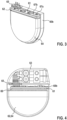
- Fig. 3 the elements of the implant are partially assembled.
- the electronic module 61 is placed on the energy storage device 62. Furthermore, the feedthrough 65 is connected to the electronic module 61.
- the energy storage device 62 (in the insulating sleeve 64) with the electronic module 61 is arranged in the second housing shell 60b.
- the first housing shell 60a is placed on the second housing shell 60b and the housing shells 60a, 60b are connected to one another, e.g. welded (not shown).
- the electrode connection device 63 is then placed on the housing 60 and connected to the feedthrough 65 (not shown).
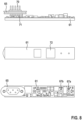
- Fig. 4 shows a side view of an implant that is essentially the same as the implant
- the electronic module 61 is arranged in a support frame 69.
- the support frame 69 is arranged on the front side of the energy storage device 62.
- the support frame 69 serves to center the energy storage device 62 in the housing 60 and presses it against the housing base. This prevents the transmission of vibrations as well as pressure and tensile forces.
- the support frame 69 thus protects the components on the electronic module 61 as well as the electrical connection between the Energy storage device 62 and the electronic module 61 from destruction and/or loss of electrical contact.
- FIG. 5 A section of the electronic module 61 is shown in Fig. 5 shown (the lower part of Fig. 5 shows an enlarged detail of the upper part).
- the feedthrough 65 is formed as a multi-pole feedthrough with several pins 70. In the embodiment shown, five pins 70 are formed on the feedthrough 65, but a different number of pins is also possible. Each pin 70 is inserted into a pin receptacle 71 in order to form an electrical connection between the electronic module 61 and the electrode connection device 63 by means of the feedthrough 65.
- the first pin element 66a, 66b (e.g. anode and cathode of the battery) is formed on the energy storage device.
- the first pin receptacle 67a, 67b is arranged on the electronic module 61.
- the electronic module 61 is electrically connected to the energy storage device 62 by means of a straight plug connection by inserting the first pin element 66a, 66b into the first pin receptacle 67a, 67b.
- the connection can be designed as a redundant connection, for example by the first pin receptacle 67a, 67b comprising two pin receptacles arranged one above the other (two rings arranged one above the other) (not shown).
- the pins 70 of the feedthrough 65 and the first pin element 66a, 66b point in the same direction (contact direction), which determines the mounting direction for the elements.
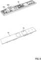
- An SMD component 72 is arranged on the back of the electronic module (cf. Fig. 8 and 9 ).
- Fig. 7 shows a block diagram of the implant.
- the functions of the electronic module are surrounded by the frame 80, which are implemented as units/chips on the electronic module and are explained in more detail below.
- a radio transceiver 81 is coupled to an antenna 82.
- the radio transceiver 81 is used for communication with an external device, in particular a programming device.
- an external device in particular a programming device.
- measured values and/or parameters of the implant can be transmitted to the programming device. Changed parameters for the implant can also be received from the programming device.
- the electronic module further comprises a control unit 83 (controller).
- the control unit 83 has a processor, e.g. a digital signal processor (DSP), a memory such as RAM (RAM - random-access memory) and/or ROM (ROM - read only memory) and a time unit (timer).
- DSP digital signal processor
- RAM random-access memory
- ROM read only memory
- timer time unit
- a memory access e.g. DMA (DMA - direct memory access) and/or network functions such as MAC (MAC - media access control) can be integrated into the control unit 83.
- DMA DMA - direct memory access
- MAC MAC - media access control
- a measuring unit 86 (sensing unit) is provided on the electronic module as a further component.
- the measuring unit 86 is configured to record measured values from the heart 91.
- a pacemaker unit 85 (pacing unit) is configured to generate stimulation pulses for the heart 91.
- the electronic module can optionally comprise a shock unit 84 (shocking unit) and an HV unit 87 (HV - high voltage), especially if the implant is designed as an ICD.
- the shock unit 84 is set up, the HV unit 87
- the HV unit 87 is configured to deliver a shock (defibrillation), for example with a voltage of 700 - 800 V.
- An EMC unit 88 (EMC - Electromagnetic Compatibility) is provided, which is designed to minimize or suppress the influence of electromagnetic fields.
- the electromagnetic fields can include interference radiation, the field of a shock delivered by the HV unit 87, the field of a stimulation pulse delivered by the pacemaker unit 85, the field of an external shock, the field of an external stimulation and fields from other external sources (e.g. a high frequency measurement).
- the EMC unit 88 is coupled to the housing 92 of the implant.
- the electronic module is coupled to a battery 90.
- An energy unit 89 of the electronic module comprises a switched-mode power supply (SMPS) and is configured for power management.
- SMPS switched-mode power supply
- the functions/units of the electronic module are implemented in various integrated circuits, i.e. in chips mounted on the electronic module.
- the dimensions of the chips are determined by their complexity of functions. The greater the complexity, the greater the planar extent of the chips.
- the size of the chips largely determines the size of the electronic module and also its orientation in the implant (parallel to the energy storage device). The size of the electronic module is also determined by the number of electrical connections between the chips, the chips with the non-integrated passive components and all other connections on the electronic module.
- Which therapy functions can be monolithically integrated on a chip using which manufacturing process or how many chips the electronic module contains depends on their operating voltage range, their data and signal complexity and their character, i.e. whether they have an analog, continuous-time or a digital, discrete-time or an analog-digital, mixed signal behavior.
- all of the functions listed above can be monolithically integrated, in particular the digital control functions, the analog-digital mixed sensing functions for ECG Signal amplification and evaluation (ECG - electrocardiogram), pacing for stimulation pulse generation, power management for optimal energy supply to the implant and shocking for voltage generation and control of the defibrillation shock.
- Manufacturing processes with the following characteristics are selected for manufacturing the integrated circuits on the electronic module: At least one chip is manufactured in a process with a minimum structure size F ⁇ 90 nm. Alternatively, at least one chip is manufactured in a process with a minimum structure size F ⁇ 65 nm. Alternatively, at least one chip is manufactured in a process with a minimum structure size F ⁇ 65 nm, on which a voltage of ⁇ 10 V can be switched simultaneously with respect to its substrate.
- At least one chip is manufactured in a process with a minimum structure size F ⁇ 65 nm, on which a voltage of ⁇ 10 V can be switched simultaneously with respect to its substrate and the SRAM memory functions (SRAM - static random-access memory, static RAM) of the chip have a capacity of ⁇ 3 megabits.
- ⁇ BGAs ball grid array packages
- PCB substrate printed circuit board substrate
- Solder balls are applied to the back of the substrate for SMD assembly.
- Packaging takes place in the panel.
- the printed circuit board substrate always has a uniform panel size for all chip sizes, which only depends on the mold tool of the transfer overmolding machine. Depending on the chip size, more or fewer chips fit on the panel, which are then sawn out of the panel in their final housing size after encapsulation and balling.
- a 205 mm x 70 mm panel has three square potting areas, each with an edge length of 56 mm, into which the chips are mounted and wire bonded (see Fig. Fig. 10A and 10B
- the application of this ⁇ TBGA packaging process to the electronic module leads to further features and extensions of the packaging process, which are described in the Fig. 10A to 10E
- the holes or fits of the cutting sleeves and/or clamping sleeves are drilled (see Fig. 10C ).
- the encapsulation not only serves to cover the chips, it is also part of the mechanical stability of the electronic module and in particular of the resulting plug connection.
- the panel is equipped with the SMD components of the electronic modules in the panel (see. Fig. 10D ).
- the edge lengths of the electronic module satisfy an integer division ratio of the potting surface edges of the panel minus the sawing losses.
- the components of the electronic module can be provided as ASICs (ASIC - application-specific integrated circuit).
- Fig. 11 shows an assembly 1 (also referred to as a header core) with a first receiving device 2 for an electrode plug and a second receiving device 13 for a further electrode plug.
- the first receiving device 2 has a front opening 6 through which the electrode plug can be inserted.
- the first receiving device 2 has a first section 3, a second section 4 and a third section 5.
- the diameter of the first section 3 is larger than the diameter of the second section 4.
- the diameter of the second section 4 is in turn larger than the diameter of the third section 5.
- the first receiving device 2 is gradually tapered from the front opening 6 to the end.
- a first connection element is formed between the first section 3 and the second section 4 (i.e. in a front area of the first receiving device 2).
- a second connection element 8 is formed between the second section 4 and the third section 5 (in a rear area of the first receiving device 2).
- Both the first connection element 7 and the second connection element 8 have at least two flat side surfaces. This enables the assembly 1 to be easily gripped during assembly and enables the assembly steps to be automated.
- the first connection element 7 and the second connection element 8 are essentially cuboid-shaped.
- the second connection element 8 has a bevelled edge 17, which serves to save material and to observe the flow direction of the epoxy resin.
- On a rear side of the first A recess 12a is formed in the plastic coating of the first connection element 7.
- a rear opening 12b is formed on a rear side of the second connection element 8.
- the assembly is partially surrounded by a plastic 11.
- the assembly is partially overmolded with polysulfone.
- Recesses for a first contact surface 9 and a second contact surface 10 are formed in the plastic 11.
- the first and second contact surfaces are formed as circular surfaces.
- a guide 16 is formed adjacent to the first and second contact surfaces 9, 10.
- the guide 16 serves to accommodate a connection element (e.g. a wiring strip).
- the guides on the contact surfaces prevent connection elements from different contact surfaces from touching one another.
- the second receiving device 13 is constructed analogously to the first receiving device 2. For reasons of clarity, the components of the second receiving device (an opening, the three step-shaped tapered sections and the two connection elements) are not provided with reference symbols.
- the second receiving device also has two contact surfaces (third contact surface 14 and fourth contact surface 15) for connections. Guides are again formed adjacent to the contact surfaces.
- a positioning device 18b is formed, which is designed as a pin with a tapered end.
- the pointed end of the positioning device 18b can be inserted into a receptacle in the housing to facilitate the precise positioning of the assembly on the housing.
- the assembly can also be designed without a positioning device 18b.
- Positioning pins 18a are formed on the underside of the assembly (cf. Fig. 12 ).
- the positioning pins can be placed in associated receptacles when arranging the assembly on the housing of the implant. In the embodiment shown, two positioning pins are shown, but other numbers of positioning pins are possible.
- the first receiving device 2 and the second receiving device 13 each have a spring sleeve and a plug receptacle.
- the first receiving device 2 and the second receiving device 13 can be designed as IS-1 connectors.
- a spring element 20 is arranged in the first receiving device 2 and fixed there (left side of Fig. 13 ).
- the recess 12a in the plastic is used to weld the spring element 20 arranged inside the first receiving device 2 into the first connection element 7 by means of resistance welding.
- another spring element is arranged and fastened in the second receiving device 13 (not shown).
- the openings of the assembly 1 are then closed and sealed with potting aids 21, 22, 23 (right side of Fig. 13 ).
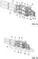
- FIG. 14 A further assembly step is shown.
- a wire band 24 is attached to the third contact surface 14 (e.g. welded).
- the wire band 24 has a wire band connection 25 which is connected to a pin contact of a feedthrough 30 (cf. Fig. 4 ) and can be plugged onto the pin contact, for example. Additional wire strips are connected to the other contact surfaces 9, 10, 15.
- An antenna 26 is attached to the assembly 1.
- the antenna 26 partially surrounds the first section 3 of the first receiving device 2 and is clipped to it.
- the antenna 26 has a U-shaped section 27. This forms a recessed grip that can be used, for example, with an automated gripper to hold and transport the assembly.
- An antenna connection 28 for connection to the feedthrough 30 is formed at a rear end of the antenna.
- the assembly with the wire bands and the antenna is then arranged in a mold (e.g. a silicone mold) (not shown).
- the wire band connections and the antenna connection 28 are plugged onto assigned pins of the feedthrough 30 and connected to the pins (e.g. welded).
- the mold is closed and filled with a synthetic resin 31 (e.g. epoxy resin). This forms the electrode connection device (see Fig. 16 ).
- the casting aids 21, 22, 23 are removed and any excess resin on the outer surfaces is removed, e.g. by grinding and/or polishing.
- the implant with the electrode connection device is now fully assembled ( Fig. 17 ).
- FIG. 18 A further embodiment of the implant is shown.
- the electrode connection device 53 is attached to a cover 121.
- the energy storage device 62 is accommodated in a housing 120.
- the housing 120 can be provided as a deep-drawn form.
- the cover 121 is welded to the housing 120 along a circumferential weld seam 122 in order to close the housing 120.
- a support frame 69 is arranged on the energy storage device.
- the support frame 69 accommodates the electronic module.
- the electrode connection device 53 can be made, for example, according to the Fig. 11 to 17 shown embodiment.
- the feedthrough 65 with the pins 70 is welded into the cover 121.
- the embodiments of the implant and methods disclosed herein may have the following advantages:
- the internal structure of the electronic implant is significantly simplified, so that manufacturing costs are reduced.
- the number and complexity of the required manufacturing processes is also reduced, so that the scalability of production is promoted (e.g. simplified transfer to other locations, low training requirements for employees, lower requirements for the required manufacturing environment and accompanying engineering).
- rework is possible or simplified when detachable connection techniques are used.
- the form factor of the electronic module allows the implant to be made smaller or the volume gained can be used to increase the battery capacity and thus extend the life of the implant.
- the production of the electronic module in ⁇ TBGA technology enables an increase in the benefit on the Panel and the associated manufacturing cost savings.
- the vertical mounting of the electronic module (parallel to the front of the energy storage device) enables electrical connections without angles and thus a simpler, more cost-effective construction of the implant optimized for automatic production in one axis.
Landscapes
- Health & Medical Sciences (AREA)
- Animal Behavior & Ethology (AREA)
- Biomedical Technology (AREA)
- Nuclear Medicine, Radiotherapy & Molecular Imaging (AREA)
- Radiology & Medical Imaging (AREA)
- Life Sciences & Earth Sciences (AREA)
- Engineering & Computer Science (AREA)
- General Health & Medical Sciences (AREA)
- Public Health (AREA)
- Veterinary Medicine (AREA)
- Electrotherapy Devices (AREA)
- Structures For Mounting Electric Components On Printed Circuit Boards (AREA)
- Prostheses (AREA)
- Non-Metallic Protective Coatings For Printed Circuits (AREA)
Abstract
Description
- Ein Implantat, wie ein Herzschrittmacher oder ein Defibrillator, enthält unter anderem ein Elektronikmodul mit Chips, eine Batterie zur Energieversorgung und eine Durchführung zu einem Header, an welchem eine oder mehrere Elektroden angeschlossen sein können. Derzeitig bekannte Kontaktierungen zwischen dem Elektronikmodul, der Batterie und der Durchführung werden üblicherweise mit angelöteten oder angeschweißten Kontaktierungsbändern realisiert. In alternativen Ausführungsformen werden gebogene Batteriepins in Steckkontaktierungen angeschlossen.
- In
Fig. 1 ist ein Implantat dargestellt, wie es aus dem Stand der Technik bekannt ist. Das Implantat umfasst ein Gehäuse 50, in dem eine Batterie 51 und ein Elektronikmodul 52 angeordnet sind. An dem Gehäuse 50 ist eine Elektrodenanschlussvorrichtung (Header) 53 angeordnet. Ein erster elektrischer Kontakt 54 ist zwischen dem Elektronikmodul 52 und der Batterie 51 gebildet. Ein zweiter elektrischer Kontakt 56 ist zwischen dem Elektronikmodul 52 und einer Durchführung 55 gebildet. Die Durchführung 55 führt aus dem Gehäuse 50 heraus und stellt eine elektrische Verbindung zwischen dem Elektronikmodul 52 und der Elektrodenanschlussvorrichtung 53 her. Die Elemente des Implantats (Elektrodenanschlussvorrichtung 53, Durchführung 55, Batterie 51 und Elektronikmodul 52) sind flach nebeneinander aneinandergereiht. Dies führt dazu, dass jede elektrische Verbindung zwischen den Elementen (insbesondere der erste elektrische Kontakt 54 und der zweite elektrische Kontakt 56) einen Winkel von 90° durchläuft und damit aufwändige und kostspielige Aufbauprozesse erfordert. Die Herstellung des inFig. 1 gezeigten Implantats erfordert komplexe Fertigungstechnologie und ist schwierig zu automatisieren. - Das Dokument
US 9,737,721 B2 - Das Dokument
US 7,647,110 B2 beschreibt ein modulares Implantat. Verschiedene Konnektormodule, Elektronikmodule und Batteriemodule können miteinander kombiniert werden, um unterschiedliche Funktionen zu realisieren. - Das Dokument
EP 2 493 557 B1 offenbart einen modularen Header für ein Implantat. Der Header ist aus mehreren Modulen aufgebaut, die miteinander verbunden sind. Mit der Anzahl der Module kann eine Länge des Headers angepasst werden. - Das Dokument
US 2018/0054034 A1 offenbart einen modularen Konnektor, dessen Länge mittels der Anzahl der eingesetzten Module angepasst werden kann. - Das Dokument
US 9,713,717 B2 - Aufgabe ist es, verbesserte Technologien für Implantate anzugeben. Insbesondere soll die Herstellung eines aktiven medizinischen Implantats vereinfacht werden.
- Es ist ein Implantat nach Anspruch 1 offenbart. Weitere Ausführungsformen sind Gegenstand von abhängigen Ansprüchen.
- Nach einem Aspekt ist ein Implantat mit einem Gehäuse bereitgestellt. In dem Gehäuse sind ein Energiespeicher und ein Elektronikmodul angeordnet. An dem Gehäuse ist eine Durchführung zu einer Elektrodenanschlussvorrichtung gebildet. Ein erster Kontakt bildet eine elektrische Verbindung zwischen dem Energiespeicher und dem Elektronikmodul. Ein zweiter Kontakt bildet eine elektrische Verbindung zwischen dem Elektronikmodul und der Durchführung. Der erste Kontakt und der zweite Kontakt sind in die gleiche Kontaktrichtung ausgerichtet.
- Das Implantat kann ein aktives medizinisches Implantat sein, beispielsweise ein implantierbarer Herzschrittmacher oder ein implantierbarer Kardioverter-Defibrillator (ICD - implantable cardioverter-defibrillator).
- Die Elektrodenanschlussvorrichtung kann auch als Anschlusskopf oder als Header bezeichnet werden. Die Elektrodenanschlussvorrichtung kann eingerichtet sein, eine oder mehrere Elektrodenanschlüsse aufnehmen.
- Das Elektronikmodul kann Komponenten aufweisen, welche den Betrieb des Implantats gewährleisten, beispielsweise einen Prozessor und einen Speicher.
- Der Energiespeicher kann eine Primärzelle, eine Sekundärzelle, einen Kondensator oder eine beliebige Kombination der vorgenannten Elemente umfassen. Der Energiespeicher kann eingerichtet sein, die Komponenten des Elektronikmoduls mit elektrischer Energie zu versorgen. Des Weiteren kann der Energiespeicher eingerichtet sein, elektrische Energie für eine Defibrillation (Schock) bereitzustellen. Der Energiespeicher kann gegenüber dem Gehäuse elektrisch isoliert sein, beispielsweise mittels einer Hülle aus einem elektrisch isolierenden Material (z. B. einem thermoplastischem Kunststoff wie PEEK, PEEK - Polyetheretherketon), einem fest anhaftenden Kunststoffüberzug aus einem elektrisch isolierenden Material, einer ein- oder mehrteiligen Isolierfolie, einer Beschichtung aus einem elektrisch isolierenden Material (z. B. Kunststoff) oder mittels Bekleben des Energiespeichers mit einer Isolierfolie.
- Die Durchführung kann eine elektrische Verbindung zwischen der Elektrodenanschlussvorrichtung und dem Elektronikmodul bereitstellen. Die Durchführung kann mehrpolig ausgeführt sein, beispielsweise dreipolig, vierpolig oder fünfpolig.
- Das Gehäuse kann ein biokompatibles Material aufweisen oder aus einem biokompatiblen Material (z. B. Titan) bestehen.
- Eine gleiche Kontaktrichtung ist gegeben, wenn eine Vorzugsrichtung des ersten Kontakts mit einer Vorzugsrichtung des zweiten Kontakts übereinstimmt, also die Kontakte in die gleiche Richtung zeigen. Die Vorzugsrichtung der Kontakte kann sich aus der Geometrie der Kontakte ergeben. Bei einem Stiftkontakt ist die Vorzugsrichtung eine Längserstreckung des Stifts. Bei einem flächigen Kontakt ist die Vorzugsrichtung die Normale der Fläche.
- Es kann vorgesehen sein, dass der Energiespeicher, das Elektronikmodul und die Durchführung in einer Stapelrichtung übereinander angeordnet sind, wobei die Stapelrichtung der Kontaktrichtung entspricht. Der Energiespeicher, das Elektronikmodul und die Durchführung werden in einer einzigen Montagerichtung montiert. Das Übereinanderstapeln der Elemente vereinfacht die Montage des Implantats und erleichtert eine Automatisierung des Herstellungsprozesses. Des Weiteren kann die Elektrodenanschlussvorrichtung in der Stapelrichtung auf dem Gehäuse angeordnet sein.
- Der erste Kontakt kann zwischen einem ersten flächigen Kontaktelement, das an dem Energiespeicher angeordnet ist, und einem zweiten flächigen Kontaktelement, das an dem Elektronikmodul angeordnet ist, gebildet sein, wobei die Kontaktrichtung die Normale einer Kontaktfläche zwischen dem ersten flächigen Kontaktelement und dem zweiten flächigen Kontaktelement ist. Das erste flächige Kontaktelement und das zweite flächige Kontaktelement können gleich groß sein. Das erste flächige Kontaktelement und das zweite flächige Kontaktelement können die gleiche Form aufweisen, beispielsweise quadratisch, rechteckig, rund oder oval. Das erste flächige Kontaktelement und das zweite flächige Kontaktelement können symmetrisch ausgebildet sein.
- Der zweite Kontakt kann zwischen einem dritten flächigen Kontaktelement, das an dem Elektronikmodul angeordnet ist, und einem vierten flächigen Kontaktelement, das an der Durchführung angeordnet ist, gebildet sein, wobei die Kontaktrichtung die Normale einer Kontaktfläche zwischen dem dritten flächigen Kontaktelement und dem vierten flächigen Kontaktelement ist. Das dritte flächige Kontaktelement und das vierte flächige Kontaktelement können gleich groß sein. Das dritte flächige Kontaktelement und das vierte flächige Kontaktelement können die gleiche Form aufweisen, beispielsweise quadratisch, rechteckig, rund oder oval. Das dritte flächige Kontaktelement und das vierte flächige Kontaktelement können symmetrisch ausgebildet sein.
- In einer Ausführungsform kann vorgesehen sein, dass der erste Kontakt zwischen einem ersten Stiftelement und einer ersten Stiftaufnahme gebildet ist, wobei eine Längserstreckung des ersten Stiftelements die Kontaktrichtung bestimmt. Das erste Stiftelement kann an dem Energiespeicher angeordnet sein. In diesem Fall ist die erste Stiftaufnahme an dem Elektronikmodul angeordnet. In einer anderen Variante kann das erste Stiftelement an dem Elektronikmodul angeordnet sein und die erste Stiftaufnahme ist an dem Energiespeicher angeordnet. Das erste Stiftelement kann mehrere Stifte umfassen, die parallel zueinander ausgerichtet sind. Es kann vorgesehen sein, dass das erste Stiftelement als ein Paar von Stiften gebildet ist, das beispielsweise an dem Energiespeicher (z. B. als Anode und Kathode des Energiespeichers) angeordnet ist. Die erste Stiftaufnahme ist in diesem Fall als ein Paar von Stiftaufnahmen gebildet, die beispielsweise an dem Elektronikmodul angeordnet sein können.
- Des Weiteren kann vorgesehen sein, dass der zweite Kontakt zwischen einem zweiten Stiftelement und einer zweiten Stiftaufnahme gebildet ist, wobei eine Längserstreckung des zweiten Stiftelements die Kontaktrichtung definiert. Das zweite Stiftelement kann an der Durchführung angeordnet sein, wobei die zweite Stiftaufnahme an dem Elektronikmodul angeordnet ist. Alternativ kann das zweite Stiftelement an dem Elektronikmodul angeordnet sein und die zweite Stiftaufnahme ist an der Durchführung angeordnet. Das zweite Stiftelement kann mehrere Stifte umfassen, die parallel zueinander ausgerichtet sind. Die mehreren Stifte können beispielsweise an der Durchführung angeordnet sein (mehrpolige Durchführung). In diesem Fall umfasst die zweite Stiftaufnahme mehrere Stiftaufnahmen, die beispielsweise an dem Elektronikmodul angeordnet sind.
- Das erste Stiftelement und das zweite Stiftelement können parallel zueinander angeordnet sein.
- Der erste Kontakt und/oder der zweite Kontakt können als Steckkontakt, Klemmkontakt oder Schweißkontakt ausgebildet sein.
- Das Elektronikmodul kann an einer Stirnseite des Energiespeichers angeordnet sein. Die Stirnseite ist die der Elektrodenanschlussvorrichtung zugewandte Seite des Energiespeichers. Das Elektronikmodul ist also zwischen der Elektrodenanschlussvorrichtung und dem Energiespeicher angeordnet.
- Das Elektronikmodul kann parallel oder senkrecht zur Stirnseite des Energiespeichers angeordnet sein. Das Elektronikmodul kann ein flächiges Substrat aufweisen, auf welchem Komponenten angeordnet sind. Bei dem flächigen Substrat ist die Höhe des Substrats sehr viel kleiner als die Breite und die Länge des Substrats. Das Substrat kann als Leiterplatte ausgebildet sein. Das flächige Substrat kann parallel oder senkrecht zur Stirnseite des Energiespeichers angeordnet sein. Insbesondere eine parallele Anordnung des Elektronikmoduls/des Substrats ermöglicht eine platzsparende Montage. In diesem Fall liegt das Elektronikmodul auf der Stirnseite des Energiespeichers.
- Es kann vorgesehen sein, dass das Elektronikmodul in einem Stützrahmen angeordnet ist. Der Stützrahmen kann derart in dem Gehäuse angeordnet sein, dass der Energiespeicher durch den Stützrahmen fixiert ist. Der Stützrahmen kann mit einem Presssitz auf dem Energiespeicher angeordnet sein, so dass der Energiespeicher von dem Stützrahmen gegen das Gehäuse gedrückt wird und hierdurch fixiert ist. Alternativ oder ergänzend kann vorgesehen sein, dass der Stützrahmen derart ausgebildet und in dem Gehäuse angeordnet ist, dass der Stützrahmen eine Relativbewegung zwischen dem Energiespeicher und dem Elektronikmodul reduziert oder verhindert. Insbesondere soll eine Relativbewegung, welche zum Verlust der elektrischen Verbindung zwischen dem Elektronikmodul und dem Energiespeicher führt, verhindert werden. Der Stützrahmen kann einen Kunststoff enthalten oder vollständig aus einem Kunststoff bestehen. Geeignete Kunststoffe sind beispielsweise Polybutylenterephthalat (PBT), Polykarbonat (PC) oder ähnliche Kunststoffe.
- Das Gehäuse kann zweiteilig gebildet sein und eine erste Gehäuseschale und eine zweite Gehäuseschale aufweisen. Es kann vorgesehen sein, dass der Energiespeicher zwischen der ersten Gehäuseschale und der zweiten Gehäuseschale fixiert ist. Die erste Gehäuseschale und die zweite Gehäuseschale können symmetrisch (z. B. spiegelsymmetrisch) oder identisch sein. Das zweiteilige Gehäuse kann einen integrierten Schweißschutz (z. B. eine Umbördelung) aufweisen.
- In einer Ausführungsform kann das Gehäuse einteilig gebildet sein. Das einteilige Gehäuse kann durch direktes Formen aus einem Grundmaterial hergestellt werden, beispielsweise mittels Tiefziehen.
- Das Gehäuse kann eine Öffnung aufweisen, wobei der Energiespeicher und das Elektronikmodul durch die Öffnung in das Gehäuse einführbar sind. Die Öffnung kann an einer Stirnseite (der Elektrodenanschlussvorrichtung zugewandten Seite) des Gehäuses gebildet sein. Wenn das Gehäuse zweiteilig ist, können die erste Gehäuseschale und die zweite Gehäuseschale miteinander verbunden sein (z. B. verschweißt), so dass die Öffnung an der Stirnseite gebildet ist. Die Öffnung kann in Kontaktrichtung geöffnet sein. In diesem Fall können alle Elemente des Implantats (der Energiespeicher, das Elektronikmodul, die Durchführung, die Elektrodenanschlussvorrichtung und das Gehäuse) in einer einzigen Stapelrichtung montiert werden.
- Der Energiespeicher kann am Gehäuse befestigt sein. Beispielsweise kann an der ersten Gehäuseschale und/oder an der zweiten Gehäuseschale ein selbstklebendes Klebepad angebracht sein, an dem/denen der Energiespeicher klebt, wenn die Gehäuseschalen zum Gehäuse verbunden sind. Es kann auch vorgesehen sein, dass der Energiespeicher mittels eines Klebers an der ersten Gehäuseschale und/oder an der zweiten Gehäuseschale geklebt ist. Die Fixierung kann auch durch eine Klemmwirkung zwischen der ersten Gehäuseschale und der zweiten Gehäuseschale realisiert sein. Es kann auch vorgesehen sein, dass das Gehäuse mit dem Energiespeicher verschweißt.
- In dem Gehäuse kann ein Klemmteil angeordnet sein, wobei das Klemmteil eingerichtet ist, den Energiespeicher gegenüber dem Gehäuse zu fixieren. Das Klemmteil kann ein einem unteren Abschnitt des Gehäuses, welcher der Stirnseite des Gehäuses gegenüber liegt, angeordnet sein. Das Klemmteil kann eingerichtet sein, den Energiespeicher zur Fixierung gegen den Stützrahmen zu drücken. Das Klemmteil kann als Feder, als Schweißschutzband oder als festes, raumfüllendes Kunststoffteil ausgeführt sein.
- Die Durchführung kann als SMD-Bauelement (SMD - surface-mounted device, oberflächenmontiertes Bauelement) auf dem Elektronikmodul befestigt sein. Ein SMD-Bauelement wird mittels einer oder mehrerer lötfähiger Anschlussflächen direkt auf eine Leiterplatte (z.B. das Substrat des Elektronikmoduls) gelötet. Mit anderen Worten: Die Durchführung ist in SMT-Technologie (SMT - surface-mounting technology, Oberflächenmontage) auf dem Elektronikmodul montiert.
- Die Durchführung kann ein zweites Substrat aufweisen. Das zweite Substrat der Durchführung, das Elektronikmodul (oder das Substrat des Elektronikmoduls) und die Stirnseite des Energiespeichers können parallel zueinander angeordnet sein.
- Nach einem weiteren Aspekt ist ein Verfahren zur Montage eines Implantats offenbart. Das Verfahren umfasst folgende Schritte: Bereitstellen eines Energiespeichers, Bereitstellen eines Elektronikmoduls, Bereitstellen einer Durchführung, Anordnen des Elektronikmoduls auf dem Energiespeicher und Anordnen der Durchführung auf dem Elektronikmodul. Hierbei werden die Durchführung, das Elektronikmodul und der Energiespeicher entlang einer gemeinsamen Montagerichtung aufeinander angeordnet. Insbesondere kann das Elektronikmodul auf einer Stirnseite des Energiespeichers angeordnet werden.
- Auf die Reihenfolge des Anordnens kommt es nicht an. Es kann zuerst das Elektronikmodul auf dem Energiespeicher angeordnet werden und anschließend die
- Durchführung auf dem Elektronikmodul. Es kann aber auch zuerst die Durchführung auf dem Elektronikmodul angeordnet werden und anschließend wird das Elektronikmodul mit der Durchführung auf dem Energiespeicher angeordnet.
- Beim Anordnen des Elektronikmoduls auf dem Energiespeicher kann eine elektrische Verbindung zwischen dem Energiespeicher und dem Elektronikmodul mit einem ersten Kontakt gebildet werden. Beim Anordnen der Durchführung auf dem Elektronikmodul kann eine elektrische Verbindung zwischen dem Elektronikmodul und der Durchführung mit einem zweiten Kontakt gebildet werden. Der erste Kontakt und der zweite Kontakt können in die gleiche Kontaktrichtung ausgerichtet sein.
- Das Verfahren kann weiterhin die folgenden Schritte umfassen: Anordnen des Energiespeichers mit dem Elektronikmodul und der Durchführung in einem Gehäuse und Verschließen des Gehäuses.
- Das Verfahren kann des Weiteren die folgenden Schritte umfassen: Anordnen einer Elektrodenanschlussvorrichtung auf dem Gehäuse und Verbinden der Elektrodenanschlussvorrichtung mit der Durchführung.
- Nach einem weiteren Aspekt ist ein Implantat mit einem Elektronikmodul und einem Energiespeicher bereitgestellt, wobei das Volumen des Elektronikmoduls kleiner als 25% des Volumens des Energiespeichers ist. Bevorzugt ist das Volumen des Elektronikmoduls kleiner als 20% des Volumens des Energiespeichers. Weiter bevorzugt ist das Volumen des Elektronikmoduls kleiner als 16% des Volumens des Energiespeichers. In einer Ausführungsform beträgt das Volumen des Energiespeichers 3,06 cm3 und das Volumen das Elektronikmoduls beträgt 0,46 cm3.
- Die Elemente des Implantats sind dreidimensionale Objekte, die jeweils eine Länge, eine Breite und eine Höhe aufweisen. Die Maße der Objekte werden immer in der gleichen Richtung bestimmt. Die Länge des Elektronikmoduls wird in die gleiche Richtung wie die Länge der Elektrodenanschlussvorrichtung und die Länge der Batterie bestimmt. Die Breite des Elektronikmoduls wird in die gleiche Richtung wie die Breite der Elektrodenanschlussvorrichtung und die Breite der Batterie bestimmt. Die Höhe des Elektronikmoduls wird in die gleiche Richtung wie die Höhe der Elektrodenanschlussvorrichtung und die Höhe der Batterie bestimmt. In der linken unteren Ecke von
Fig. 2 ist zur Veranschaulichung ein Koordinatensystem eingezeichnet. Die x-Richtung entspricht der Länge, die y-Richtung gibt die Breite an und die z-Richtung entspricht der Höhe. - Das Volumen des Energiespeichers ist das tatsächliche Volumen des Elements.
- Als Volumen des Elektronikmoduls wird das Volumen einer Einhüllenden um das Elektronikmodul angesehen, wobei die Grundfläche der Einhüllenden der Fläche des Elektronikmoduls entspricht und die Höhe der Einhüllenden der Höhe der höchsten Komponente auf dem Elektronikmodul entspricht. Wenn das Elektronikmodul eine rechteckige Grundfläche hat, wird das Volumen also durch einen Quader angegeben, wobei die Grundfläche des Quaders der Grundfläche des Elektronikmoduls (Produkt aus der Länge und der Breite) entspricht. Die Höhe des Quaders entspricht der Höhe der höchsten Komponente auf dem Elektronikmodul. Wenn das Elektronikmodul als flächiges Substrat ausgeführt ist, können auf einer Seite des Substrats Komponenten angeordnet sein. In diesem Fall greift die obige Definition für das Volumen. Es kann auch vorgesehen sein, dass auf beiden Seiten des Substrats Komponenten angeordnet sind. In diesem Fall entspricht die Höhe des Elektronikmoduls der Summe der Höhen der jeweils höchsten Komponente auf den beiden Seiten des Substrats.
- Das Verhältnis der Länge des Elektronikmoduls zu der Breite des Elektronikmoduls kann 4:1 oder mehr betragen, bevorzugt 5:1 oder mehr, weiter bevorzugt 6:1 oder mehr. In dieser Ausführungsform hat das Elektronikmodul eine schmale Bauform, was an Anordnen des Elektronikmoduls auf der Stirnseite des Energiespeichers erleichtern kann. In einer Ausführungsform hat das Elektronikmodul eine Länge von mehr als 30 mm und eine Breite von weniger als 5,2 mm.
- Es kann vorgesehen sein, dass die Breite des Elektronikmoduls kleiner oder gleich der Breite des Energiespeichers ist.
- Die Länge des Elektronikmoduls kann kleiner oder gleich der Länge des Energiespeichers sein.
- Wie oben schon erläutert, kann das Implantat eine Elektrodenanschlussvorrichtung aufweisen, wobei die Länge des Elektronikmoduls kleiner oder gleich der Länge der Elektrodenanschlussvorrichtung ist und/oder wobei die Breite des Elektronikmoduls kleiner oder gleich der Breite der Elektrodenanschlussvorrichtung ist. Es kann auch vorgesehen sein, dass die Länge des Energiespeichers kleiner oder gleich der Länge der Elektrodenanschlussvorrichtung ist und/oder dass die Breite des Energiespeichers kleiner oder gleich der Breite der Elektrodenanschlussvorrichtung ist.
- Das Elektronikmodul kann ein Substrat aufweisen, auf welchem mehrere Komponenten angeordnet sind, wobei die Fläche des Substrats kleiner oder gleich der Fläche der Stirnseite des Energiespeichers ist.
- Es kann vorgesehen sein, dass einige der mehreren Komponenten eine minimale Strukturgröße von F ≤ 90 nm aufweisen. Alternativ oder ergänzend kann vorgesehen sein, dass einige (oder andere) der mehreren Komponente eine minimale Strukturgröße von F ≤ 65 nm, bevorzugt F ≤ 55 nm, aufweisen. Es können alle Komponenten des Elektronikmoduls mit einer einheitlichen Strukturgröße gefertigt sein, beispielsweise F ≤ 90 nm, F ≤ 65 nm oder F ≤ 55 nm. Es kann auch vorgesehen sein, dass die Komponenten des Elektronikmoduls mit verschiedenen der hier genannten Strukturgrößen gefertigt sind.
- Wenigstens eine der mehreren Komponenten kann auf einer ersten Seite des Substrats angeordnet sein und wenigstens eine andere der mehreren Komponenten kann auf einer zweiten Seite des Substrats angeordnet sein. Das Substrat kann also einseitig oder zweiseitig bestückt sein.
- In einer Ausführungsform kann vorgesehen sein, dass die wenigstens eine Komponente auf der ersten Seite des Substrats und/oder die wenigstens eine andere Komponente auf der zweiten Seite des Substrats mit einem Vergussmittel verkapselt sind.
- Es kann vorgesehen sein, dass einige der mehreren Komponenten als SMD-Elemente auf dem Substrat angeordnet sind. Die Komponenten können beispielsweise in einem oder mehreren Ball Grid Array (BGA) und/oder Multi Chip Modul (MCM) Gehäusen und/oder als nackte integrierte Schaltungen (Chips) angeordnet sein. Bei einer einseitigen Bestückung des Substrats sind folgende Anordnungen der Komponenten möglich:
- alle Komponenten sind in einem Ball Grid Array Gehäuse angeordnet,
- alle Komponenten sind in einem MCM Gehäuse angeordnet,
- alle Komponenten sind als Chips angeordnet,
- alle Komponenten sind als SMD-Elemente angeordnet und
- eine oder einige oder keine Komponenten sind in einem oder mehreren BGA Gehäusen angeordnet, eine oder einige oder keine der anderen Komponenten sind in einem oder mehreren MCM Gehäusen angeordnet, eine oder einige oder keine der anderen Komponenten sind als Chips angeordnet und eine oder einige oder keine der anderen Komponenten sind als SMD-Elemente angeordnet.
- Bei einer zweiseitigen Bestückung des Substrats können die oben aufgeführten Anordnungen für beide Seiten des Substrats realisiert sein.
- Es kann vorgesehen sein, dass einige der mehreren Komponenten auf einer Seite des Substrats nebeneinander oder übereinander angeordnet sind, wobei die Chips/Komponenten jeweils mit dem Substrat verbunden sind und wobei die Komponenten mit einem Vergussmittel verkapselt sind. Die Verbindung der Chips/Komponenten mit dem Substrat kann als Wire-Bonds, Flip Chip Bumps oder Flip-Chip-Lötballen-Verbindung ausgeführt sein. Das Vergussmittel kann das Substrat teilweise bedecken. Das Vergussmittel kann sich in einer Ausführungsform entlang einer Kante des Substrats erstrecken. Bevorzugt bedeckt das Vergussmittel vollständig die Seite des Substrats, auf welcher die Komponenten angeordnet sind.
- Auf einem als Substrat dienenden Paneel können die Komponenten gitterförmig angeordnet werden, derart, dass jede Gitterzelle alle für ein Elektronikmodul erforderlichen Einheiten/Chips aufweist. Jede(r) Chip/Komponente wird an das Substrat gebondet, um die elektrischen Verbindungen herzustellen. Anschließend wird das Paneel mit einem Vergussmittel verkapselt (Overmoulding). Nachdem das Paneel mit dem Vergussmittel bedeckt ist, werden die einzelnen Elektronikmodule aus dem Paneel gesägt. Vorteilhafterweise ist die Länge der Vergussfläche auf Paneel ein ganzzahliges Vielfaches der Länge des Elektronikmoduls und/oder die Breite der Vergussbereiches auf dem Paneel ist ein ganzzahliges Vielfaches der Breite des Elektronikmoduls. Hierdurch wird die Vergussfläche des Pannels optimal ausgenutzt. Auf einer anderen Seite des Paneels/Substrats können weitere Komponenten angeordnet sein, beispielsweise als SMD-Elemente, in Chips und/oder in Ball Grid Array Gehäusen.
- In dem Vergussmittel können Löcher für einen Anschlusskontakt für den Energiespeicher und/oder für einen weiteren Anschlusskontakt für eine Durchführung gebildet sein.
- Das Elektronikmodul kann als ein Multi-Chip-Modul gebildet sein. Ein Multi-Chip-Modul (MCM) besteht aus mehreren einzelnen Mikrochips, die in einem gemeinsamen Gehäuse planar (nebeneinander) oder übereinander untergebracht sind und nach außen wie ein Chip aussehen, so funktionieren und eingesetzt werden.
- Die Durchführung zu der Elektrodenanschlussvorrichtung kann als
- integrale Komponente des Elektronikmoduls,
- SMD-Bauelement auf dem Elektronikmodul oder
- Steckverbindung auf dem Elektronikmodul gebildet sein.
- Gemäß einem weiteren Aspekt ist Implantat mit einem Elektronikmodul und einer elektronischen Komponente bereitgestellt, wobei eine elektrische Verbindung zwischen dem Elektronikmodul und der elektronischen Komponente mit einer geraden Steckverbindung gebildet ist.
- Das Implantat kann eine weitere elektronische Komponente aufweisen, wobei eine elektrische Verbindung zwischen dem Elektronikmodul und der weiteren elektronischen Komponente mit einer weiteren geraden Steckverbindung gebildet ist und wobei die gerade Steckverbindung und die weitere gerade Steckverbindung in die gleiche Richtung orientiert sind. Die hier offenbarten Merkmale für die gerade Steckverbindung gelten analog für die weitere gerade Steckverbindung. Ebenso gelten die Ausführungen zu der elektronischen Komponente analog für die weitere elektronische Komponente.
- Die elektrische Verbindung kann ganz oder teilweise als Steckkontakt derart ausgebildet sein, dass ein Kontaktpin (oder mehrere Kontaktpins) der elektronischen Komponente direkt in eine Steckeraufnahme des Elektronikmoduls auf- oder durchgesteckt werden kann. Die gerade Steckverbindung ist frei von einem Adapter (z.B. einem Verdrahtungsband); des Weiteren ist eine Abwinkelung des Pins nicht notwendig.
- Die elektronische Komponente oder die weitere elektronische Komponente können eine Durchführung oder ein Energiespeicher sein. Es können mehrere elektronische Komponenten vorgesehen sein, wobei für jede elektronische Komponente eine elektrische Verbindung mit dem Elektronikmodul mit einer geraden Steckverbindung gebildet ist. Das Elektronikmodul und die elektronische(n) Komponente(n) können in einem Gehäuse angeordnet sein.
- In einer Ausführungsform kann ein weiteres Elektronikmodul auf dem Elektronikmodul angeordnet sein. Das weitere Elektronikmodul kann mittels einer geraden Steckverbindung mit dem Elektronikmodul verbunden sein. Es kann ein Stapel von mehreren Elektronikmodulen gebildet sein, wobei die mehreren Elektronikmodule jeweils mit einer geraden Steckverbindung miteinander verbunden sind.
- Die elektronische Komponente kann ein gerades Stiftelement aufweisen, wobei das Elektronikmodul eine Stiftaufnahme aufweist, und wobei das Stiftelement in der Stiftaufnahme angeordnet ist, um die elektrische Verbindung zu bilden.
- Alternativ kann das Elektronikmodul ein gerades Stiftelement aufweisen, wobei die elektronische Komponente eine Stiftaufnahme aufweist, und wobei das Stiftelement in der Stiftaufnahme angeordnet ist, um die elektrische Verbindung zu bilden.
- Wie bereits ausgeführt kann das gerade Stiftelement mehrere Stifte umfassen. Die mehreren Stifte können parallel zueinander angeordnet sein. In diesem Fall sind mehrere Stiftaufnahmen vorgesehen, wobei jeder der mehreren Stifte jeweils einer der mehreren Stiftaufnahmen zugeordnet ist.
- Die Stiftaufnahme kann ringförmig sein. Die Stiftaufnahme kann als Scheibe ausgeführt sein. Die Stiftaufnahme kann auf das Elektronikmodul oder auf die elektronische Komponente gelötet sein. Das Stiftelement kann in der Stiftaufnahme verschweißt sein.
- Die Stiftaufnahme kann mit einer der folgenden Befestigungsarten an dem Elektronikmodul befestigt sein: Löten, Kleben, Einbetten, Klemmen und Crimpen. Unter Crimpen versteht man ein Fügeverfahren, bei dem zwei Bauteile durch plastische Verformung miteinander verbunden werden, beispielsweise durch Bördeln, Quetschen, Kräuseln oder Falten. Beim Einbetten ist ein Teil der Stiftaufnahme vom Material des Elektronikmoduls umschlossen.
- Die Stiftaufnahme kann mit einer der folgenden Befestigungsarten an der elektronischen Komponente befestigt sein: Löten, Kleben, Einbetten, Klemmen und Crimpen.
- Es kann vorgesehen sein, dass das Stiftelement ein Federelement aufweist.
- Die elektronische Komponente kann ein Energiespeicher, eine Durchführung oder ein Kondensator sein. Die elektronische Komponente kann des Weiteren als Hochspannungskondensator oder als Kondensatorstapel ausgeführt sein. In einer Ausführungsform ist die elektronische Komponente ein Energiespeicher und die weitere elektronische Komponente ist eine Durchführung.
- Die Steckverbindung kann als lösbare Verbindung gebildet sein, z. B. als Steckverbindung.
- Die Steckverbindung kann als nicht lösbare Verbindung gebildet sein, z. B. als Schweißverbindung oder Lötverbindung.
- Die elektrische Verbindung kann mit einer Verbindung ausgewählt aus den folgenden Verbindungsarten gebildet sein: Federkontakt, Schneidklemmkontakt, Lötkontakt, Schweißkontakt, Presspassung und Kleben. Für eine Klebeverbindung kann ein elektrisch leitfähiger Kleber verwendet werden.
- Die Steckverbindung kann ausgebildet sein, eine Relativbewegung zwischen der elektronischen Komponente und dem Elektronikmodul auszugleichen, ohne dass die elektrische Verbindung unterbrochen wird. Beispielsweise kann das Stiftelement hinreichend lang und flexibel ausgeführt sein, um eine Relativbewegung der elektronischen Komponente gegenüber dem Elektronikmodul auszugleichen. Alternativ oder ergänzend kann die Steckeraufnahme hinreichend flexibel ausgeführt und/oder montiert sein, um eine Relativbewegung der elektronischen Komponente gegenüber dem Elektronikmodul auszugleichen. Beispielsweise kann das Stiftelement eine Länge aufweisen, die größer ist als eine Höhe der Stiftaufnahme. In diesem Fall ragt das Stiftelement im eingesteckten Zustand über die Stiftaufnahme hinaus, so dass eine Bewegung entlang der Richtung des Stiftelements in einem gewissen Bereich ausgeglichen werden kann.
- Gemäß noch einem anderen Aspekt ist ein Verfahren zum Herstellen einer elektrischen Verbindung zwischen einem Elektronikmodul und einer elektronischen Komponente eines Implantats bereitgestellt, wobei die elektronische Komponente und das Elektronikmodul mit einer Relativbewegung aufeinander zu bewegt werden, und die elektrische Verbindung mit einer geraden Steckverbindung zwischen der elektronischen Komponente und dem Elektronikmodul gebildet wird. Die Relativbewegung kann eine gerade Relativbewegung sein. Dies erleichtert die Umsetzung eines automatisierten Prozesses zur Montage des Implantats.
- Die Steckverbindung kann als redundante Verbindung ausgeführt sein, um die Zuverlässigkeit zu erhöhen.
- Nach noch einem weiteren Aspekt ist ein Implantat mit einer Elektrodenanschlussvorrichtung und einem Gehäuse offenbart, wobei an der Elektrodenanschlussvorrichtung ein Deckel zum Verschluss des Gehäuses gebildet ist.
- Der Deckel kann mit dem Gehäuse verschweißt sein. Es kann vorgesehen sein, dass an dem Deckel ein Flansch gebildet ist. Der Flansch kann einen Umfang des Deckels teilweise oder vollständig umlaufen.
- An dem Deckel kann eine Schweißschutzeinrichtung gebildet sein, beispielsweise in Form einer teilweise oder vollständig umlaufenden Umbördelung.
- Der Deckel kann alternativ mittels einer Steckverbindung, einer Federverbindung oder einer Klemmverbindung an dem Gehäuse befestigt sein.
- Der Deckel kann aus einem biokompatiblen Material gebildet sein, beispielsweise Titan.
- Der Deckel und das Gehäuse können aus dem gleichen Material gebildet sein (z. B. Titan).
- Im Deckel kann eine Durchführung gebildet sein, wobei die Durchführung eine elektrische Verbindung zwischen der Elektrodenanschlussvorrichtung und einem in dem Gehäuse angeordneten Elektronikmodul bildet.
- Die Durchführung kann mit einer Steckverbindung oder mit einem Federkontakt mit dem Elektronikmodul elektrisch verbunden sein.
- Die Elektrodenanschlussvorrichtung kann eine vormontierte Baugruppe aufweisen. Die Baugruppe kann folgende Bauelemente umfassen: eine durchgehende Aufnahmeeinrichtung für einen Stecker, ein erstes Anschlusselement, das in einem vorderen Bereich der Aufnahmeeinrichtung angeordnet ist, wobei das erste Anschlusselement wenigstens zwei ebene Seitenflächen aufweist, und ein zweites Anschlusselement, das in einem hinteren Bereich der Aufnahmeeinrichtung angeordnet ist, wobei das zweite Anschlusselement wenigstens zwei ebene Seitenflächen aufweist.
- Nach einem weiteren Aspekt ist eine Baugruppe für eine Elektrodenanschlussvorrichtung eines Implantats bereitgestellt. Die Baugruppe umfasst eine durchgehende Aufnahmeeinrichtung für einen Stecker. Des Weiteren ist ein erstes Anschlusselement vorgesehen, das in einem vorderen Bereich der Aufnahmeeinrichtung angeordnet ist, wobei das erste Anschlusselement wenigstens zwei ebene Seitenflächen aufweist. Schließlich ist ein zweites Anschlusselement vorgesehen, das in einem hinteren Bereich der Aufnahmeeinrichtung angeordnet ist, wobei das zweite Anschlusselement wenigstens zwei ebene Seitenflächen aufweist.
- Des Weiteren ist eine Elektrodenanschlussvorrichtung für ein Implantat mit einer hier offenbarten Baugruppe bereitgestellt.
- Die Offenbarung umfasst des Weiteren ein Implantat mit einer Elektrodenanschlussvorrichtung und einer Baugruppe.
- Die ebenen Seitenflächen ermöglichen eine zumindest teilweise eckige Form und erlauben ein einfaches Greifen der Baugruppe (manuell oder automatisch). Hierdurch kann eine Automatisierung des Herstellungsprozesses ermöglicht werden.
- Die Baugruppe kann zumindest abschnittsweise von einem Kunststoff umgeben sein. Beispielsweise kann die Baugruppe von dem Kunststoff abschnittsweise umspritzt sein. Der Kunststoff kann ein Thermoplast sein, beispielsweise Polysulfon. Es kann auch ein biokompatibles Gießharz verwendet werden. Der Kunststoff kann der Baugruppe zusätzliche Stabilität verleihen. Hiermit ist es möglich, die Baugruppe als vorgefertigte Komponente herzustellen, welche anschließend zu einer Elektrodenanschlussvorrichtung eines Implantats verarbeitet wird.
- Ein Anschlussbereich des ersten Anschlusselements kann frei von Kunststoff sein. Alternativ oder ergänzend kann ein Anschlussbereich des zweiten Anschlusselements frei von Kunststoff sein.
- In dem Kunststoff kann eine erste Führung für einen ersten Leiter zum Anschluss an den Anschlussbereich des ersten Anschlusselements gebildet sein und/oder in dem Kunststoff kann eine zweite Führung für einen zweiten Leiter zum Anschluss an den Anschlussbereich des zweiten Anschlusselements gebildet sein.
- Die erste Führung kann benachbart zu dem Anschlussbereich des ersten Anschlusselements gebildet sein und/oder die zweite Führung kann benachbart zu dem Anschlussbereich des zweiten Anschlusselements gebildet sein.
- An den Anschlussbereich des ersten Anschlusselements (des zweiten Anschlusselements) kann an erster Leiter (zweiter Leiter) angeschlossen werden, um eine Verbindung von einem in die Aufnahmeeinrichtung eingeführten Stecker zu einem Implantat zu ermöglichen. Der Anschlussbereich des ersten Anschlusselements und/oder der Anschlussbereich des zweiten Anschlusselements können als flächige Elemente ausgeführt sein. Der Anschlussbereich des ersten Anschlusselements und/oder der Anschlussbereich des zweiten Anschlusselements können kreisförmig gebildet sein und beispielsweise einen Durchmesser von 1 bis 5 mm haben. Hierdurch ist eine große Schweißfläche zum Befestigen des ersten Leiters bzw. des zweiten Leiters gegeben. In einer Ausführungsform sind sowohl die erste Führung als auch die zweite Führung benachbart zu den jeweiligen Anschlussbereichen gebildet. Die Führungen ermöglichen einen Anschluss der Leiter an die jeweiligen Anschlussbereiche, ohne einen Kurzschluss zu verursachen.
- Es kann vorgesehen sein, dass das erste Anschlusselement und das zweite Anschlusselement zueinander versetzt angeordnet sind. Mit anderen Worten, das erste Anschlusselement und das zweite Anschlusselement liegen auf zwei verschiedenen Ebenen. Die unterschiedliche Anordnung erleichtert es, die Leiter an die Anschlusselemente anzuschließen, ohne dass die Leiter miteinander in Kontakt kommen.
- In einer Ausführungsform kann die Baugruppe eine Antenne aufweisen, wobei die Antenne in einem Zwischenbereich, der zwischen dem ersten Anschlusselement und dem zweiten Anschlusselement gebildet ist, einen U-förmigen Verlauf hat. Der Zwischenbereich kann schmaler ausgebildet sein als die angrenzenden Anschlusselemente. Zusammen mit dem U-förmigen Verlauf der Antenne ist hierdurch eine Greifmulde für einen automatischen Greifer gebildet.
- An einem hinteren Ende der Aufnahmeeinrichtung kann eine Positioniereinrichtung gebildet sein. Die Positioniereinrichtung kann als abgewinkelte Struktur gebildet sein und beispielsweise einen rechten Winkel zu der Aufnahmeeinrichtung bilden. Die Positioniereinrichtung kann aus dem Kunststoff gebildet sein und beispielsweise mit dem Kunststoffüberzug der Baugruppe einteilig gebildet sein. Die Positioniereinrichtung kann beim Anordnen der Baugruppe in eine Aufnahme an einem Gehäuse des Implantats angeordnet werden, um das Ausrichten der Baugruppe zu erleichtern. Die Positioniereinrichtung kann ein spitz zulaufendes Ende haben.
- Die Baugruppe kann eine weitere Aufnahmeeinrichtung für einen weiteren Stecker aufweisen, wobei in einem vorderen Bereich der weiteren Aufnahmeeinrichtung ein drittes Anschlusselement angeordnet ist, und wobei in einem hinteren Bereich der weiteren Aufnahmeeinrichtung ein viertes Anschlusselement angeordnet ist. Für die weitere Aufnahmeeinrichtung gelten die hier offenbarten Ausführungen zu der Aufnahmeeinrichtung analog. Des Weiteren gelten für das dritte Anschlusselement und das vierte Anschlusselement die Ausführungen zum ersten Anschlusselement und zum zweiten Anschlusselement analog.
- Nach einem weiteren Aspekt ist ein Verfahren zum Bilden einer Elektrodenanschlussvorrichtung auf einem Implantat offenbart. Das Verfahren umfasst folgende Schritte:
- Bereitstellen einer Baugruppe, mit
- einer durchgehenden Aufnahmeeinrichtung für einen Stecker,
- einem ersten Anschlusselement, das in einem vorderen Bereich der Aufnahmeeinrichtung angeordnet ist, wobei das erste Anschlusselement wenigstens zwei ebene Seitenflächen aufweist, und
- einem zweiten Anschlusselement, das in einem hinteren Bereich der Aufnahmeeinrichtung angeordnet ist, wobei das zweite Anschlusselement wenigstens zwei ebene Seitenflächen aufweist,
- Anordnen und Befestigen eines Federelements in der Aufnahmeeinrichtung,
- Verschließen von Öffnungen der Aufnahmeeinrichtung mit Vergusshilfsmitteln,
- Befestigen eines ersten Leiters an dem ersten Anschlusselement,
- Befestigen eines zweiten Leiters an dem zweiten Anschlusselement,
- Anordnen der Baugruppe auf einem Gehäuse des Implantats,
- Verbinden des ersten Leiters mit einer Durchführung, die an einem Gehäuse gebildet ist,
- Verbinden des zweiten Leiters mit der Durchführung,
- Anordnen der Baugruppe mit dem Gehäuse in einer Gießform,
- Füllen der Gießform mit einem Kunstharz,
- nach Aushärten des Kunstharzes, Entfernen der Vergusshilfsmittel.
- Mit dem Verfahren kann ebenfalls eine Elektrodenanschlussvorrichtung auf einem Deckel eines Implantats gebildet werden.
- Das Verfahren kann die weiteren Schritte umfassen:
- Anordnen und Befestigen einer Antenne an der Baugruppe,
- Verbinden der Antenne mit der Durchführung,
- Des Weiteren kann vorgesehen sein, nach dem Aushärten eventuell überstehendes Harz zu entfernen, beispielsweise mittels Schleifen und/oder Polieren.
- Die Gießform kann eine Silikonform sein.
- Die Durchführung kann einen oder mehrere Steckkontakte (z.B. Stifte) zum Anschluss der Leiter und/oder der Antenne aufweisen.
- Das Kunstharz kann ein Epoxidharz sein. Epoxidharze sind Kunstharze, die Epoxidgruppen tragen. Sie sind härtbare Harze (Reaktionsharze), die mit einem Härter und gegebenenfalls weiteren Zusatzstoffen zu einem duroplastischen Kunststoff umgesetzt werden können. Epoxidharze sind Polyether mit zwei endständigen Epoxidgruppen. Die Härtungsmittel sind Reaktionspartner und bilden zusammen mit dem Harz einen makromolekularen Kunststoff.
- Das Kunstharz kann direkt auf dem Gehäuse des Implantats oder auf dem Deckel des Implantats haften, so dass ein zusätzliches Haftmittel nicht erforderlich ist. Mit anderen Worten, die Kontaktfläche zwischen dem ausgehärteten Kunstharz und dem Gehäuse / Deckel des Implantats kann frei von einem Haftmittel sein.
- Die Elektrodenanschlussvorrichtung kann ein Header für einen implantierbaren Herzschrittmacher oder einen implantierbaren Kardioverter-Defibrillator (ICD - Implantable Cardioverter Defibrillator) sein. In diesem Fall dient die Elektrodenanschlussvorrichtung zur elektrischen Verbindung von einer oder mehreren Elektrodenleitungen mit dem Implantat.
- In der Elektrodenanschlussvorrichtung können eine Antenne, eine Ladespule, ein Röntgenmarker, eine Kommunikationsspule und/oder eine Farbmarkierung angeordnet sein.
- Ein weiterer Aspekt betrifft ein Verfahren zum Herstellen eines Implantats, mit folgenden Schritten: Bereitstellen eines Gehäuses, Bereitstellen einer Elektrodenanschlussvorrichtung, wobei an der Elektrodenanschlussvorrichtung ein Deckel zum Verschluss des Gehäuses gebildet ist, Anordnen des Deckels auf dem Gehäuse und Verbinden des Deckels mit dem Gehäuse. Die Verbindung zwischen dem Deckel und dem Gehäuse kann als stoffschlüssige Verbindung gebildet sein, beispielsweise mittels Schweißen.
- Die hier offenbarten Aspekte zum Implantat und zu der Baugruppe für die Elektrodenanschlussvorrichtung sowie die Aspekte zu den Verfahren können in beliebiger Weise miteinander kombiniert werden, um verschiedene Ausführungsformen des Implantats bzw. der Verfahren zu realisieren. Des Weiteren gelten die Ausführungen zum Implantat und zur Baugruppe analog für die Verfahren und anders herum.
- Im Folgenden werden beispielhafte Ausführungsformen unter Bezugnahme auf Figuren näher erläutert. Es zeigen:
- Fig. 1
- eine schematische Darstellung eines Implantats gemäß dem Stand der Technik,
- Fig. 2
- eine Explosionsdarstellung einer Ausführungsform eines erfindungsgemäßen Implantats,
- Fig. 3
- eine perspektivische Ansicht eines Teils des Implantats nach
Fig. 2 , - Fig. 4
- eine Seitenansicht eines Implantats,
- Fig. 5
- einen Ausschnitt des Elektronikmoduls,
- Fig. 6
- einen weiteren Ausschnitt des Elektronikmoduls,
- Fig. 7
- ein Blockschaltbild des erfindungsgemäßen Implantats,
- Fig. 8
- eine Seitenansicht des Elektronikmoduls (obere Abbildung von
Fig. 8 ), eine Ansicht des Elektronikmoduls von unten (mittlere Abbildung vonFig. 8 ) und eine Ansicht des Elektronikmoduls von oben (untere Abbildung vonFig. 8 ), - Fig. 9
- eine perspektivische Ansicht der Oberseite des Elektronikmoduls (obere Abbildung von
Fig. 9 ) und eine perspektivische Ansicht der Unterseite des Elektronikmoduls (untere Abbildung vonFig. 9 ), - Fig. 10A - 10E
- Schritte eines Herstellungsprozesses für das Elektronikmodul,
- Fig. 11
- eine perspektivische Ansicht einer Ausführungsform einer Baugruppe für eine Elektrodenanschlussvorrichtung,
- Fig. 12
- eine Vorderansicht (obere Abbildung von
Fig. 12 ) und eine Hinteransicht (untere Abbildung vonFig. 12 ) der Baugruppe nachFig. 11 , - Fig. 13
- die Baugruppe nach
Fig. 11 und12 mit Vergusshilfsmitteln, - Fig. 14
- die Baugruppe nach
Fig. 11 bis 13 mit einer Antenne und Leitern, - Fig. 15
- die Baugruppe nach
Fig. 11 bis 14 auf einem Gehäuse angeordnet, - Fig. 16
- die Baugruppe nach
Fig. 11 bis 15 vollständig vergossen (mit Vergusshilfsmitteln), - Fig. 17
- die Baugruppe nach
Fig. 11 bis 15 vollständig vergossen (ohne Vergusshilfsmittel) und - Fig. 18
- eine weitere Ausführungsform eines erfindungsgemäßen Implantats.
-
Fig. 2 zeigt eine Ausführungsform eines Implantats gemäß der Erfindung. Das Implantat umfasst ein zweiteiliges Gehäuse 60 mit einer ersten Gehäuseschale 60a und einer zweiten Gehäuseschale 60b. In dem Gehäuse 60 sind ein Elektronikmodul 61 und ein Energiespeicher 62 (z. B. eine Batterie) angeordnet. Der Energiespeicher 62 ist mittels einer Isolierhülle 64 von dem Gehäuse 60 elektrisch isoliert. Das Elektronikmodul 61 ist auf einer Stirnseite 68 des Energiespeichers 62 angeordnet. An der Stirnseite 68 des Energiespeichers 62 ist ein erstes Stiftelement angeordnet, das zwei parallel zueinander ausgerichtete Stifte 66a, 66b umfasst. Dem ersten Stiftelement ist eine erste Stiftaufnahme zugeordnet, die zwei ringförmige Stiftaufnahmen 67a, 67b umfasst und die an dem Elektronikmodul 61 angeordnet ist. Mittels des ersten Stiftelements 66a, 66b und der ersten Stiftaufnahme 67a, 67b ist eine elektrische Verbindung zwischen dem Energiespeicher 62 und dem Elektronikmodul 61 gebildet. Das Elektronikmodul 61 ist mit einer Durchführung 65 verbunden. Details zu der Verbindung werden weiter unten näher erläutert. Auf dem Gehäuse 60 ist eine Elektrodenanschlussvorrichtung 63 angeordnet, die mittels der Durchführung 65 mit dem Elektronikmodul 61 verbunden ist. - Die Durchführung 65, das Elektronikmodul 61 und der Energiespeicher 62 werden entlang einer Achse montiert (hier entlang der z-Richtung). Die Richtung der Achse ist durch die Richtung der elektrischen Verbindung zwischen der Durchführung 65 und dem Elektronikmodul 61 sowie der elektrischen Verbindung zwischen dem Elektronikmodul 61 und dem Energiespeicher 62 bestimmt.
- In der gezeigten Ausführungsform ist das Elektronikmodul 61 parallel zur Stirnseite 68 des Energiespeichers 62 angeordnet. Diese Art der Anordnung nutzt den Raum im Gehäuse sehr effizient. Das Elektronikmodul 61 kann auf die Stirnseite 68 des Energiespeichers 62 aufgesteckt werden und/oder mit der Stirnseite 68 verklebt sein.
- In
Fig. 3 sind die Elemente des Implantats teilweise montiert. Das Elektronikmodul 61 ist auf den Energiespeicher 62 aufgesetzt. Des Weiteren ist die Durchführung 65 mit dem Elektronikmodul 61 verbunden. Der Energiespeicher 62 (in der Isolierhülle 64) mit dem Elektronikmodul 61 ist in der zweiten Gehäuseschale 60b angeordnet. Im nächsten Schritt wird die erste Gehäuseschale 60a auf der zweiten Gehäuseschale 60b angeordnet und die Gehäuseschalen 60a, 60b werden miteinander verbunden, z.B. verschweißt (nicht dargestellt). Anschließend wird die Elektrodenanschlussvorrichtung 63 auf das Gehäuse 60 gesetzt und mit der Durchführung 65 verbunden (nicht dargestellt). -
Fig. 4 zeigt eine Seitenansicht eines Implantats, das im Wesentlichen dem Implantat nach -
Fig. 2 entspricht. Gleiche Elemente sind daher mit gleichen Bezugszeichen bezeichnet. Bei der Ausführungsform nachFig. 4 ist das Elektronikmodul 61 in einem Stützrahmen 69 angeordnet. Der Stützrahmen 69 ist auf der Stirnseite des Energiespeichers 62 angeordnet. Der Stützrahmen 69 dient der Zentrierung des Energiespeichers 62 im Gehäuse 60 und presst diese gegen den Gehäuseboden. Dies verhindert die Weiterleitung von Vibrationen sowie von Druck- und Zugkräften. Der Stützrahmen 69 schützt somit die Komponenten auf dem Elektronikmodul 61 sowie die elektrische Verbindung zwischen dem Energiespeicher 62 und dem Elektronikmodul 61 vor Zerstörung und/oder elektrischem Kontaktverlust. - Ein Ausschnitt des Elektronikmoduls 61 ist in
Fig. 5 dargestellt (der untere Teil vonFig. 5 zeigt einen vergrößerten Ausschnitt des oberen Teils). Die Durchführung 65 ist als mehrpolige Durchführung mit mehreren Pins 70 gebildet. In der gezeigten Ausführungsform sind fünf Pins 70 an der Durchführung 65 gebildet, eine andere Anzahl von Pins ist jedoch ebenfalls möglich. Jeder Pin 70 steckt in einer Pinaufnahme 71, um mittels der Durchführung 65 eine elektrische Verbindung zwischen dem Elektronikmodul 61 und der Elektrodenanschlussvorrichtung 63 zu bilden. - Ein weiterer Ausschnitt des Elektronikmoduls zusammen mit einem Ausschnitt des Energiespeichers 62 ist in
Fig. 6 gezeigt. An dem Energiespeicher ist das erste Stiftelement 66a, 66b (z. B. Anode und Kathode der Batterie) gebildet. Auf dem Elektronikmodul 61 ist die erste Stiftaufnahme 67a, 67b angeordnet. Das Elektronikmodul 61 wird mit dem Energiespeicher 62 mittels einer geraden Steckverbindung elektrisch verbunden, indem das erste Stiftelement 66a, 66b in die erste Stiftaufnahme 67a, 67b eingeführt wird. Die Verbindung kann als redundante Verbindung ausgeführt sein, beispielweise indem die erste Stiftaufnahme 67a, 67b jeweils zwei übereinander angeordnete Stiftaufnahmen (zwei übereinander angeordnete Ringe) umfasst (nicht dargestellt). - Die elektrische Verbindung zwischen dem Elektronikmodul 61 und dem Energiespeicher 62 kann mit folgenden Technologien realisiert werden:
- als Zylinder mit Bohrung mit Laserschweißen (vgl.
Fig. 6 ), - als Federkontakt in einer Steckverbindung und
- als Winkel auf dem Elektronikmodul mit Widerstandsschweißen.
- Die Pins 70 der Durchführung 65 sowie das erste Stiftelement 66a, 66b zeigen in die gleiche Richtung (Kontaktrichtung), welche die Montagerichtung für die Elemente bestimmt.
- Auf einer Rückseite des Elektronikmoduls ist ein SMD-Bauelement 72 angeordnet (vgl.
Fig. 8 und9 ). -
Fig. 7 zeigt ein Blockschaltbild des Implantats. Die Funktionen des Elektronikmoduls sind von dem Rahmen 80 umgeben, die als Einheiten / Chips auf dem Elektronikmodul realisiert sind und im Folgenden näher erläutert werden. - Ein Radio-Transceiver 81 ist mit einer Antenne 82 gekoppelt. Der Radio-Transceiver 81 dient zur Kommunikation mit einem externen Gerät, insbesondere einem Programmiergerät. Hierbei können beispielsweise Messwerte und/oder Parameter des Implantats an das Programmiergerät übertragen werden. Es können auch geänderte Parameter für das Implantat vom Programmiergerät empfangen werden.
- Das Elektronikmodul umfasst des Weiteren eine Steuereinheit 83 (Controller). Die Steuereinheit 83 weist einen Prozessor auf, z. B. einen digitalen Signalprozessor (DSP - digital signal processor), einen Speicher wie RAM (RAM - random-access memory, Direktzugriffsspeicher) und/oder ROM (ROM - read only memory, Nur-Lese-Speicher) und eine Zeiteinheit (Timer). Als weitere Funktionen können ein Speicherzugriff, z.B. DMA (DMA - direct memory access, Speicherdirektzugriff) und/oder Netzwerkfunktionen wie MAC (MAC - media access control, Medienzugriffssteuerung) in die Steuereinheit 83 integriert sein.
- Als weitere Komponente ist eine Messeinheit 86 (Sensing-Einheit) auf dem Elektronikmodul vorgesehen. Die Messeinheit 86 ist konfiguriert, Messwerte vom Herzen 91 aufzunehmen.
- Eine Schrittmachereinheit 85 (Pacing-Einheit) ist konfiguriert, Stimulationsimpulse für das Herz 91 zu erzeugen.
- Das Elektronikmodul kann optional eine Schockeinheit 84 (Shocking-Einheit) und eine HV-Einheit 87 (HV - high voltage, Hochspannung) umfassen, insbesondere wenn das Implantat als ICD ausgeführt ist. Die Schockeinheit 84 ist eingerichtet, die HV-Einheit 87 zu steuern. Die HV-Einheit 87 ist konfiguriert, einen Schock abzugeben (Defibrillation), beispielsweise mit einer Spannung von 700 - 800 V.
- Es ist eine EMV-Einheit 88 (EMV - Elektromagnetische Verträglichkeit) vorgesehen, die eingerichtet ist, den Einfluss von elektro-magnetischen Feldern zu minimieren oder zu unterdrücken. Die elektro-magnetischen Felder können Störstrahlung, das Feld eines von der HV-Einheit 87 abgegebenen Schocks, das Feld eines von der Schrittmachereinheit 85 abgegebenen Stimulationspulses, das Feld eines externen Schocks, das Feld einer externen Stimulation und Felder anderer externer Quellen (z. B. einer Hochfrequenzmessung) umfassen. Die EMV-Einheit 88 ist mit dem Gehäuse 92 des Implantats gekoppelt.
- Das Elektronikmodul ist mit einer Batterie 90 gekoppelt. Eine Energieeinheit 89 des Elektronikmoduls umfasst ein Schaltnetzteil (SMPS - switched-mode power supply) und ist für ein Powermanagement konfiguriert.
- Die Funktionen/Einheiten des Elektronikmoduls sind in verschiedenen integrierten Schaltungen, d. h. in auf dem Elektronikmodul montierten Chips, implementiert. Die Abmessungen der Chips ergeben sich durch ihre Komplexität an Funktionen. Je höher die Komplexität, umso größer ist die planare Ausdehnung der Chips. Die Größe der Chips bestimmt maßgeblich die Größe des Elektronikmoduls und auch dessen Ausrichtung im Implantat (parallel zum Energiespeicher). Auch wird die Größe des Elektronikmoduls bestimmt durch die Anzahl der elektrischen Verbindungen der Chips untereinander, der Chips mit den nicht integrierten passiven Komponenten und alle weiteren Verbindungen auf dem Elektronikmodul.
- Welche Therapiefunktionen mit welchem Herstellungsprozess miteinander auf einem Chip monolithisch integriert werden können oder wie viele Chips das Elektronikmodul enthält, hängt von ihrem Arbeitsspannungsbereich, ihrer Daten- und Signalkomplexität sowie von ihrem Charakter ab, d.h. ob sie ein analoges, zeitkontinuierliches oder ein digitales, zeitdiskretes oder ein analog-digital, gemischtes Signalverhalten haben. Im Prinzip können alle oben aufgeführten Funktionen monolithisch integriert werden, insbesondere die digitalen Steuerfunktionen, die analog-digital gemischten Sensing Funktionen zur EKG Signalverstärkung und -bewertung (EKG - Elektrokardiogramm), das Pacing zur Stimulationspulserzeugung, das Powermanagement zur optimalen Energieversorgung des Implantates und das Shocking zur Spannungserzeugung und Steuerung des Defibrillationsschockes. Mit den derzeit verwendeten Herstellungsprozessen mit minimalen Strukturgrößen F = 130 nm und F = 180 nm resultieren jedoch Chips, deren Abmessung zu groß für eine vertikale Anordnung im Implantatgehäuse sind und darüber hinaus deren Datenspeicherkapazität (RAM) zu klein ist bzw. mit einem weiteren Speicherchip ergänzt werden muss, um alle erforderten Therapie- und Diagnosefunktionen zu ermöglichen. Für das vorliegende Implantat werden daher einige oder alle Funktionen des Elektronikmoduls mit Chips implementiert, die mit einer minimalen Strukturgröße F ≤ 90 nm, bevorzugt F ≤ 65 nm oder F ≤ 55 nm, hergestellt werden.
- Ein Ziel ist es, dass Elektronikmodul derart auszugestalten, dass es Volumen, Form und Größe des Implantates nicht mehr bestimmt (wie im Stand der Technik). Dazu wird mindestens eine der folgenden Regeln angewandt:
- 1. Das Elektronikmodul wird parallel zur Stirnseite des Energiespeichers angeordnet.
- 2. Die Länge des Elektronikmoduls ist kleiner oder gleich der Länge der Elektrodenanschlussvorrichtung.
- 3. Die Breite des Elektronikmoduls ist kleiner oder gleich der Breite des Energiespeichers (oder der Breite des Gehäuses).
- 4. Die Länge des Energiespeichers ist gleich der Länge der Elektrodenanschlussvorrichtung (maximale Volumenausnutzung).
- 5. Die Fläche des Elektronikmoduls entspricht der Fläche der Stirnseite des Energiespeichers.
- 6. Der Volumenbedarf des Elektronikmodules beträgt weniger als 1/4 des Volumens des Energiespeichers (oder weniger als 1/4 des gesamten metallumhüllenden Volumen des Implantates).
- Bei Anwendung einer oder mehrerer dieser Regeln entsteht ein streifenförmiges, schmales Elektronikmodul, das mit Komponenten bestückt wird, deren maximale Kantenlänge inklusive ihrer Anschlussverbindungen das Elektronikmodul nicht überragt. Durch verbesserte optischen Abbildungen und Lithographie-Verfahren in der Halbleiterherstellung wird immer mehr Funktionalität pro Siliziumfläche ermöglicht. Eine für die Herstellung des Implantats ausreichende minimale Strukturgröße der Komponenten ist F ≤ 90 nm. Dies ermöglicht es, Analog-, Digital-, Analog-Digital gemischte und Hochspannungsschaltungen zunehmend auf einem Chip monolithisch zu intergieren. Hierdurch wird die Anzahl der Chips und die Anzahl der Verbindungen auf dem Elektronikmodul reduziert, womit die kleinere zur Verfügung stehende Fläche des nun schmalen, streifenförmigen Modules wieder kompensiert wird, um die bekannte funktionale Komplexität zu ermöglichen.
- Für die Herstellung der integrierten Schaltungen auf dem Elektronikmodul werden Herstellungsprozesse mit folgenden Merkmalen ausgewählt: Es wird mindestens ein Chip in einem Prozess mit minimaler Strukturgröße F ≤ 90 nm hergestellt. Alternativ wird mindestens ein Chip in einem Prozess mit minimaler Strukturgröße F ≤ 65 nm hergestellt. Alternativ wird mindestens ein Chip in einem Prozess mit minimaler Strukturgröße F ≤ 65 nm hergestellt, auf dem gleichzeitig eine Spannung von ≥ 10 V bezüglich seines Substrates geschaltet werden kann. Alternativ wird mindestens ein Chip in einem Prozess mit minimaler Strukturgröße F ≤ 65 nm hergestellt, auf dem gleichzeitig eine Spannung von ≥ 10 V bezüglich seines Substrates geschaltet werden kann und die SRAM Speicherfunktionen (SRAM - static random-access memory, statisches RAM) des Chips hat eine Kapazität von ≥ 3 Megabit.
- Das Elektronikmodul mit dem hier beschrieben Formfaktor eignet sich für eine Montage im Querschnitt des flachen Implantates, insbesondere zwischen dem Energiespeicher und der Elektrodenanschlussvorrichtung. Durch diesen Montageort ergeben sich weitere Merkmale des Elektronikmoduls, die einzeln oder in beliebiger Kombination miteinander realisiert werden können:
- senkrechte Anschlüsse für bedrahtete Komponenten auf der Oberseite und/oder Unterseite Elektronikmoduls,
- Bohrungen zum Auf- oder Durchstecken von Anschlüssen von Komponenten, z. B. Batterieanschlüsse und/oder Headeranschlüsse,
- eine Bohrpassung zur Aufnahme von Schneidhülsen und/oder Klemmhülsen.
- Gesägte, gerade Kanten ermöglichen auch eine optimale Fertigung des Elektronikmoduls im Nutzen in einer standardmäßigen Verpackungstechnologie für Ball Grid Array Packages (µBGAs). Beim µTBGA werden die Chips auf ein Leiterplattensubstrat (PCB Substrat) montiert, gebondet und mit einer Moldmasse in einem Transferovermoldprozess abgedeckt. Auf der Rückseite des Substrates werden Lötkugeln aufgebracht zur SMD Montage. Die Verpackung findet im Nutzen statt. Dabei hat das Leiterplattensubstrat für alle Chipgrößen immer eine einheitliche Paneelgröße, die nur vom Gussformwerkzeug der Transferovermoldmaschine abhängt. Je nach Chipgröße passen mehr oder weniger viele Chips auf das Panel, die dann nach dem Verguss und dem Bekugeln in ihrer endgültigen Gehäusegröße vom Paneel ausgesägt werden.
- In einer Ausführungsform befinden sich auf einem 205 mm x 70 mm großen Paneel drei quadratische Vergussflächen mit je 56 mm Kantenlänge, in die die Chips montiert und drahtgebondet werden (vgl.
Fig. 10A und 10B ). Die Anwendung dieses µTBGA Verpackungsprozesses auf das Elektronikmodul führt zu weiteren Kennzeichen und Erweiterungen des Verpackungsprozesses, die in denFig. 10A bis 10E dargestellt sind. Nach dem Transfermolden werden die Löcher oder Passungen der Schneidhülsen und/oder Klemmhülsen gebohrt (vgl.Fig. 10C ). Der Verguss dient nicht nur zur Abdeckung der Chips, er ist auch Teil der mechanischen Stabilität des Elektronikmoduls und insbesondere der resultierenden Steckverbindung. Anstelle der Lötkugeln wird das Paneel mit den SMD-Bauelementen der Elektronikmodule im Nutzen bestückt (vgl.Fig. 10D ). Die Kantenlängen des Elektronikmoduls erfüllt ein ganzzahliges Teilerverhältnis der Vergussflächenkanten des Paneels abzüglich der Sägeverluste. Die Komponenten des Elektronikmoduls können als ASICs (ASIC - application-specific integrated circuit, anwendungsspezifische integrierte Schaltung) bereitgestellt sein. - Einige Herstellungsschritte sind im Folgenden nochmal zusammengefasst:
-
Fig. 10A : ASICs 101 werden im Nutzen auf einer ersten Seite (Vorderseite) des Paneels 100 montiert und gebondet. -
Fig. 10B : Transferovermolding der monierten ASICs 101 mit einem Vergussmittel 102. -
Fig. 10C : Bohren der Löcher 103 für einen Anschluss des Energiespeichers. -
Fig. 10D : Bestückung einer zweiten Seite (Rückseite) des Panels 100 mit SMD-Bauelementen 104. -
Fig. 10E : Aussägen der fertigen Elektronikmodule. - In den
Fig. 11 bis 17 sind die einzelnen Schritte zur Montage einer Elektrodenanschlussvorrichtung (Header) auf einem Implantat dargestellt. Die Schritte werden im Folgenden näher erläutert. -
Fig. 11 zeigt eine Baugruppe 1 (auch als Headerkern bezeichnet) mit einer ersten Aufnahmeeinrichtung 2 für einen Elektrodenstecker und einer zweiten Aufnahmeeinrichtung 13 für einen weiteren Elektrodenstecker. Die erste Aufnahmeeinrichtung 2 weist eine vordere Öffnung 6 auf, durch welche der Elektrodenstecker eingeführt werden kann. Die erste Aufnahmeeinrichtung 2 weist einen ersten Abschnitt 3, einen zweiten Abschnitt 4 und einen dritten Abschnitt 5 auf. Der Durchmesser des ersten Abschnitts 3 ist größer als der Durchmesser des zweiten Abschnitts 4. Der Durchmesser des zweiten Abschnitts 4 ist wiederum größer als der Durchmesser des dritten Abschnitts 5. Mit anderen Worten: die erste Aufnahmeeinrichtung 2 ist von der vorderen Öffnung 6 zum Ende hin stufenweise verjüngt. - Zwischen dem ersten Abschnitt 3 und dem zweiten Abschnitt 4 (also in einem vorderen Bereich der ersten Aufnahmeeinrichtung 2) ist ein erstes Anschlusselement gebildet. Zwischen dem zweiten Abschnitt 4 und dem dritten Abschnitt 5 (in einem hinteren Bereich der ersten Aufnahmeeinrichtung 2) ist ein zweites Anschlusselement 8 gebildet. Sowohl das erste Anschlusselement 7 als auch das zweite Anschlusselement 8 weisen mindestens zwei ebene Seitenflächen auf. Dies ermöglicht ein einfaches Greifen der Baugruppe 1 während einer Montage und ermöglicht eine Automatisierung der Montageschritte. In der dargestellten Ausführungsform sind das erste Anschlusselement 7 und das zweite Anschlusselement 8 im Wesentlichen quaderförmig gebildet. Das zweite Anschlusselement 8 weist eine abgeschrägte Kante 17 auf, welche zur Materialeinsparung und zur Beachtung der Fließrichtung des Epoxidharzes dient. An einer Rückseite des ersten Anschlusselements 7 ist eine Aussparung 12a in dem Kunststoffüberzug gebildet. An einer Rückseite des zweiten Anschlusselements 8 ist eine hintere Öffnung 12b gebildet.
- Die Baugruppe ist zum Teil von einem Kunststoff 11 umgeben. In der dargestellten Ausführungsform ist die Baugruppe teilweise mit Polysulfon umspritzt. In dem Kunststoff 11 sind Aussparungen für eine erste Kontaktfläche 9 und eine zweite Kontaktfläche 10 gebildet. Die erste und zweite Kontaktfläche sind als kreisförmige Flächen gebildet. Benachbart zu der ersten und zweiten Kontaktfläche 9, 10 ist jeweils eine Führung 16 gebildet. Die Führung 16 dient zur Aufnahme eines Anschlusselements (z.B. eines Verdrahtungsbandes). Die Führungen an den Kontaktflächen verhindern, dass Anschlusselemente von verschiedenen Kontaktflächen einander berühren.
- Die zweite Aufnahmeeinrichtung 13 ist analog zu der ersten Aufnahmeeinrichtung 2 aufgebaut. Aus Gründen der Übersichtlichkeit sind die Komponenten der zweiten Aufnahmeeinrichtung (eine Öffnung, die drei stufenförmig verjüngenden Abschnitte sowie die zwei Anschlusselemente) nicht mit Bezugszeichen versehen. Die zweite Aufnahmeeinrichtung weist ebenfalls zwei Kontaktflächen (dritte Kontaktfläche 14 und vierte Kontaktfläche 15) für Anschlüsse auf. Benachbart zu den Kontaktflächen sind wiederum Führungen gebildet.
- An einem Ende der zweiten Aufnahmeeinrichtung ist eine Positioniereinrichtung 18b gebildet, welche als Zapfen mit einem spitz zulaufenden Ende ausgeführt ist. Beim Montieren der Baugruppe 1 auf einem Gehäuse 29 (vgl.
Fig. 15 ) kann das spitze Ende der Positioniereinrichtung 18b in eine Aufnahme des Gehäuses eingesetzt werden, um das passgenaue Anordnen der Baugruppe auf dem Gehäuse zu erleichtern. Die Baugruppe kann jedoch auch ohne Positioniereinrichtung 18b ausgeführt sein. - An einer Unterseite der Baugruppe sind Positionierstifte 18a gebildet (vgl.
Fig. 12 ). Die Positionierstifte können beim Anordnen der Baugruppe auf dem Gehäuse des Implantats in zugeordneten Aufnahmen angeordnet werden. In der gezeigten Ausführungsform sind zwei Positionierstifte gezeigt, andere Zahlen von Positionierstiften sind jedoch möglich. - Die erste Aufnahmeeinrichtung 2 und die zweite Aufnahmeeinrichtung 13 weisen jeweils eine Federhülse und eine Steckeraufnahme auf. Die erste Aufnahmeeinrichtung 2 und die zweite Aufnahmeeinrichtung 13 können als IS-1 Konnektoren ausgebildet sein.
- Ein Federelement 20 wird in der ersten Aufnahmeeinrichtung 2 angeordnet und dort befestigt (linke Seite von
Fig. 13 ). Die Aussparung 12a in dem Kunststoff wird genutzt, um das im Inneren der ersten Aufnahmeeinrichtung 2 angeordnete Federelement 20 mittels Widerstandsschweißen in das erste Anschlusselement 7 einzuschweißen. Analog wird ein weiteres Federelement in der zweiten Aufnahmeeinrichtung 13 angeordnet und befestigt (nicht dargestellt). Die Öffnungen der Baugruppe 1 werden anschließend mit Vergusshilfsmitteln 21, 22, 23 verschlossen und abgedichtet (rechte Seite vonFig. 13 ). - In
Fig. 14 ist ein weiterer Montageschritt gezeigt. Ein Drahtband 24 ist an der dritten Kontaktfläche 14 befestigt (z.B. verschweißt). An seinem hinteren Ende weist das Drahtband 24 einen Drahtbandanschluss 25 auf, der mit einem Stiftkontakt einer Durchführung 30 (vgl.Fig. 4 ) verbindbar ist und beispielsweise auf den Stiftkontakt aufgesteckt werden kann. Weitere Drahtbänder sind mit den anderen Kontaktflächen 9, 10, 15 verbunden. - An der Baugruppe 1 ist eine Antenne 26 befestigt. Die Antenne 26 umgreift den ersten Abschnitt 3 der ersten Aufnahmeeinrichtung 2 teilweise und ist hieran geklippt. In einem Bereich zwischen dem ersten Anschlusselement 7 und dem zweiten Anschlusselement 8 weist die Antenne 26 einen U-förmigen Abschnitt 27 auf. Hierdurch ist eine Griffmulde gebildet, die beispielsweise mit einem automatisierten Greifer verwendet werden kann, um die Baugruppe zu halten und zu transportieren. An einem hinteren Ende der Antenne ist ein Antennenanschluss 28 zur Verbindung mit der Durchführung 30 gebildet.
- Die Baugruppe mit den Drahtbändern und der Antenne wird anschließend in einer Gießform (z. B. eine Silikonform) angeordnet (nicht dargestellt). Die Drahtbandanschlüsse und der Antennenanschluss 28 werden auf zugeordnete Stifte der Durchführung 30 gesteckt und mit den Stiften verbunden (z. B. verschweißt). Die Gießform wird verschlossen und mit einem Kunstharz 31 (z. B. Epoxidharz) gefüllt. Hierdurch wird die Elektrodenanschlussvorrichtung abgeformt (vgl.
Fig. 16 ). - Die Vergusshilfsmittel 21, 22, 23 werden entfernt und ggf. überschüssiges Harz an den Außenflächen entfernt, z. B. mittels Schleifen und/oder Polieren. Das Implantat mit der Elektrodenanschlussvorrichtung ist hiermit fertig montiert (
Fig. 17 ). - In
Fig. 18 ist eine weitere Ausführungsform des Implantats dargestellt. Die Elektrodenanschlussvorrichtung 53 ist an einem Deckel 121 befestigt. Der Energiespeicher 62 ist einem Gehäuse 120 aufgenommen. Das Gehäuse 120 kann als tiefgezogene Form bereitgestellt werden. Der Deckel 121 wird mit dem Gehäuse 120 entlang einer umlaufenden Schweißnaht 122 verschweißt, um das Gehäuse 120 zu schließen. Auf dem Energiespeicher ist ein Stützrahmen 69 angeordnet. Der Stützrahmen 69 nimmt das Elektronikmodul auf. Die Elektrodenanschlussvorrichtung 53 kann beispielsweise gemäß der in denFig. 11 bis 17 gezeigten Ausführungsform gebildet sein. Die Durchführung 65 mit den Pins 70 ist in den Deckel 121 eingeschweißt. - Die hier offenbarten Ausführungsformen des Implantats und der Verfahren können die folgenden Vorteile aufweisen:
Der Innenaufbau des elektronischen Implantats wird deutlich vereinfacht, so dass Herstellkosten sinken. Ebenso sinkt die Anzahl und Komplexität der benötigten Herstellprozesse, so dass die Skalierbarkeit der Herstellung begünstigt wird (z.B. der vereinfachte Transfer an andere Standorte, geringer Trainingsbedarf für Mitarbeiter, geringere Anforderungen an die benötigte Fertigungsumgebung und begleitendes Engineering). Ferner werden Nacharbeiten möglich oder vereinfacht, wenn lösbare Verbindungstechniken eingesetzt werden. - Mit dem Formfaktor des Elektronikmoduls lässt sich das Implantat verkleinern oder es kann das gewonnene Volumen zur Batteriekapazitätsvergrößerung und damit zur Lebensdauerverlängerung des Implantates verwendet werden. Die Herstellung des Elektronikmoduls in µTBGA Technologie ermöglicht eine Steigerung des Nutzens auf dem Panel und eine damit einhergehende Fertigungskostenersparnis. Die vertikale Montage des Elektronikmodules (parallel zur Stirnseite des Energiespeichers) ermöglicht elektrische Verbindungen ohne Winkel und damit einen einfacheren, preisgünstigeren Aufbau des Implantates optimiert für automatische Fertigung in einer Achse.
- Die in der Beschreibung, den Ansprüchen und den Figuren offenbarten Merkmale können für die Verwirklichung von Ausführungsformen sowohl einzeln als auch in beliebiger Kombination miteinander relevant sein.
Claims (15)
- Implantat mit einem Elektronikmodul und einem Energiespeicher, wobei das Volumen des Elektronikmoduls kleiner als 25% des Volumens des Energiespeichers ist.
- Implantat nach Anspruch 1, wobei das Verhältnis der Länge des Elektronikmoduls zu der Breite des Elektronikmoduls 4:1 oder mehr beträgt.
- Implantat nach Anspruch 1 oder 2, wobei die Breite des Elektronikmoduls kleiner oder gleich der Breite des Energiespeichers ist.
- Implantat nach einem der vorangehenden Ansprüche, wobei die Länge des Elektronikmoduls kleiner oder gleich der Länge des Energiespeichers ist.
- Implantat nach einem der vorangehenden Ansprüche, ferner eine Elektrodenanschlussvorrichtung aufweisend, wobei die Länge des Elektronikmoduls kleiner oder gleich der Länge der Elektrodenanschlussvorrichtung ist und/oder wobei die Breite des Elektronikmoduls kleiner oder gleich der Breite der Elektrodenanschlussvorrichtung ist.
- Implantat nach Anspruch 5, wobei die Länge des Energiespeichers kleiner oder gleich der Länge der Elektrodenanschlussvorrichtung ist und/oder wobei die Breite des Energiespeichers kleiner oder gleich der Breite der Elektrodenanschlussvorrichtung ist.
- Implantat nach einem der vorangehenden Ansprüche, wobei das Elektronikmodul ein Substrat aufweist, auf welchem mehrere Komponenten angeordnet sind, wobei die Fläche des Substrats kleiner oder gleich der Fläche einer Stirnseite des Energiespeichers ist.
- Implantat nach Anspruch 7, wobei einige der mehreren Komponenten eine minimale Strukturgröße von F ≤ 90 nm aufweisen.
- Implantat nach Anspruch 7 oder 8, wobei wenigstens eine der mehreren Komponenten auf einer ersten Seite des Substrats angeordnet ist und wobei wenigstens eine andere der mehreren Komponenten auf einer zweiten Seite des Substrats angeordnet ist.
- Implantat nach einem der Ansprüche 7 bis 9, wobei einige der mehreren Komponenten als SMD-Elemente auf dem Substrat angeordnet sind.
- Implantat nach Anspruch 10, wobei einige der mehreren Komponenten in einem oder mehreren Ball Grid Array (BGA) Gehäusen und/oder Multi Chip Modul (MCM) Gehäusen und/oder als nackte integrierte Schaltungen auf dem Substrat angeordnet sind.
- Implantat nach einem der Ansprüche 7 bis 9, wobei einige der mehreren Komponenten auf einer Seite des Substrats nebeneinander oder übereinander angeordnet sind, wobei die Komponenten jeweils mit dem Substrat verbunden sind und wobei die Komponenten mit einem Vergussmittel verkapselt sind.
- Implantat nach Anspruch 12, wobei in dem Vergussmittel Löcher für einen Anschlusskontakt für den Energiespeicher und/oder für einen weiteren Anschlusskontakt für eine Durchführung gebildet sind.
- Implantat nach einem der vorangehenden Ansprüche, wobei das Elektronikmodul als ein Multi-Chip-Modul gebildet ist.
- Implantat nach einem der Ansprüche 5 bis 14 soweit auf Anspruch 5 rückbezogen, wobei eine Durchführung zu der Elektrodenanschlussvorrichtung als- integrale Komponente des Elektronikmoduls,- SMD-Komponente auf dem Elektronikmodul oder- Steckverbindung auf dem Elektronikmodul
gebildet ist.
Applications Claiming Priority (3)
| Application Number | Priority Date | Filing Date | Title |
|---|---|---|---|
| EP18187090.8A EP3603740A1 (de) | 2018-08-02 | 2018-08-02 | Implantat |
| PCT/EP2019/069616 WO2020025366A1 (de) | 2018-08-02 | 2019-07-22 | Implantat |
| EP19748484.3A EP3829705B1 (de) | 2018-08-02 | 2019-07-22 | Implantat |
Related Parent Applications (2)
| Application Number | Title | Priority Date | Filing Date |
|---|---|---|---|
| EP19748484.3A Division-Into EP3829705B1 (de) | 2018-08-02 | 2019-07-22 | Implantat |
| EP19748484.3A Division EP3829705B1 (de) | 2018-08-02 | 2019-07-22 | Implantat |
Publications (2)
| Publication Number | Publication Date |
|---|---|
| EP4477257A2 true EP4477257A2 (de) | 2024-12-18 |
| EP4477257A3 EP4477257A3 (de) | 2024-12-25 |
Family
ID=63143086
Family Applications (3)
| Application Number | Title | Priority Date | Filing Date |
|---|---|---|---|
| EP18187090.8A Withdrawn EP3603740A1 (de) | 2018-08-02 | 2018-08-02 | Implantat |
| EP24209372.2A Pending EP4477257A3 (de) | 2018-08-02 | 2019-07-22 | Implantat |
| EP19748484.3A Active EP3829705B1 (de) | 2018-08-02 | 2019-07-22 | Implantat |
Family Applications Before (1)
| Application Number | Title | Priority Date | Filing Date |
|---|---|---|---|
| EP18187090.8A Withdrawn EP3603740A1 (de) | 2018-08-02 | 2018-08-02 | Implantat |
Family Applications After (1)
| Application Number | Title | Priority Date | Filing Date |
|---|---|---|---|
| EP19748484.3A Active EP3829705B1 (de) | 2018-08-02 | 2019-07-22 | Implantat |
Country Status (6)
| Country | Link |
|---|---|
| US (1) | US11672993B2 (de) |
| EP (3) | EP3603740A1 (de) |
| JP (2) | JP2021532902A (de) |
| CN (1) | CN112533669A (de) |
| SG (1) | SG11202100976YA (de) |
| WO (1) | WO2020025366A1 (de) |
Citations (5)
| Publication number | Priority date | Publication date | Assignee | Title |
|---|---|---|---|---|
| US7647110B2 (en) | 2002-04-30 | 2010-01-12 | St. Jude Medical Ab | Modular implantable medical device and manufacturing method therefor |
| EP2493557B1 (de) | 2009-10-30 | 2017-05-17 | Medtronic, Inc. | Kopfteile einer implantierbaren medizinischen vorrichtung für konfigurationsvarianten der vorrichtung und elektroden |
| US9713717B2 (en) | 2013-12-09 | 2017-07-25 | Boston Scientific Neuromodulation Corporation | Implantable stimulator device having components embedded in a circuit board |
| US9737721B2 (en) | 2013-09-05 | 2017-08-22 | Boston Scientific Neuromodulation Corporation | Construction for an implantable medical device having a battery affixed to the case |
| US20180054034A1 (en) | 2009-10-30 | 2018-02-22 | Medtronic, Inc. | Implantable medical devices including elongated conductor bodies that facilitate device and lead configuration variants |
Family Cites Families (14)
| Publication number | Priority date | Publication date | Assignee | Title |
|---|---|---|---|---|
| US5144946A (en) * | 1991-08-05 | 1992-09-08 | Siemens Pacesetter, Inc. | Combined pacemaker substrate and electrical interconnect and method of assembly |
| US6567703B1 (en) * | 2000-11-08 | 2003-05-20 | Medtronic, Inc. | Implantable medical device incorporating miniaturized circuit module |
| ATE460753T1 (de) * | 2001-07-19 | 2010-03-15 | Greatbatch Ltd | Gewölbtes gehäuse für eine implantierbare medizinische vorrichtung |
| US7437193B2 (en) * | 2002-06-28 | 2008-10-14 | Boston Scientific Neuromodulation Corporation | Microstimulator employing improved recharging reporting and telemetry techniques |
| EP2329860B1 (de) * | 2009-12-03 | 2015-09-02 | Biotronik CRM Patent AG | Anschlussgehäuse und dessen Herstellung |
| CN102397625A (zh) * | 2010-09-15 | 2012-04-04 | 鼎迈医疗科技(苏州)有限公司 | 植入式有源电子装置及电刺激系统 |
| EP2535926A3 (de) * | 2011-06-17 | 2015-08-05 | BIOTRONIK SE & Co. KG | Halbleiterpaket |
| US8649869B2 (en) * | 2012-03-05 | 2014-02-11 | Pacesetter, Inc. | Implantable medical device having feedthru assembly with header side bunched conductor array and can side linear conductor array |
| US8843215B2 (en) * | 2012-06-13 | 2014-09-23 | Biotronik Se & Co. Kg | Connecting device |
| US10431345B2 (en) * | 2014-06-13 | 2019-10-01 | City Labs, Inc. | Small form factor betavoltaic battery for use in applications requiring a volumetrically-small power source |
| AU2014315492B2 (en) * | 2013-09-05 | 2017-04-20 | Boston Scientific Neuromodulation Corporation | Construction for an implantable medical device having a battery affixed to the case |
| AU2014315486B2 (en) * | 2013-09-05 | 2016-12-22 | Boston Scientific Neuromodulation Corporation | Construction for an implantable medical device employing an internal support structure |
| US9992866B2 (en) * | 2015-03-31 | 2018-06-05 | Biotronik Se & Co. Kg | Printed circuit board arrangement and electronic device having a printed circuit board device |
| CN110234392B (zh) * | 2017-01-26 | 2023-08-11 | 心脏起搏器股份公司 | 具有被包覆模制的组件的无引线装置 |
-
2018
- 2018-08-02 EP EP18187090.8A patent/EP3603740A1/de not_active Withdrawn
-
2019
- 2019-07-22 JP JP2021505725A patent/JP2021532902A/ja active Pending
- 2019-07-22 EP EP24209372.2A patent/EP4477257A3/de active Pending
- 2019-07-22 CN CN201980051641.0A patent/CN112533669A/zh active Pending
- 2019-07-22 WO PCT/EP2019/069616 patent/WO2020025366A1/de not_active Ceased
- 2019-07-22 EP EP19748484.3A patent/EP3829705B1/de active Active
- 2019-07-22 SG SG11202100976YA patent/SG11202100976YA/en unknown
- 2019-07-22 US US17/264,022 patent/US11672993B2/en active Active
-
2024
- 2024-04-08 JP JP2024062231A patent/JP2024086816A/ja active Pending
Patent Citations (5)
| Publication number | Priority date | Publication date | Assignee | Title |
|---|---|---|---|---|
| US7647110B2 (en) | 2002-04-30 | 2010-01-12 | St. Jude Medical Ab | Modular implantable medical device and manufacturing method therefor |
| EP2493557B1 (de) | 2009-10-30 | 2017-05-17 | Medtronic, Inc. | Kopfteile einer implantierbaren medizinischen vorrichtung für konfigurationsvarianten der vorrichtung und elektroden |
| US20180054034A1 (en) | 2009-10-30 | 2018-02-22 | Medtronic, Inc. | Implantable medical devices including elongated conductor bodies that facilitate device and lead configuration variants |
| US9737721B2 (en) | 2013-09-05 | 2017-08-22 | Boston Scientific Neuromodulation Corporation | Construction for an implantable medical device having a battery affixed to the case |
| US9713717B2 (en) | 2013-12-09 | 2017-07-25 | Boston Scientific Neuromodulation Corporation | Implantable stimulator device having components embedded in a circuit board |
Also Published As
| Publication number | Publication date |
|---|---|
| EP3829705A1 (de) | 2021-06-09 |
| WO2020025366A1 (de) | 2020-02-06 |
| US11672993B2 (en) | 2023-06-13 |
| JP2024086816A (ja) | 2024-06-28 |
| EP3829705B1 (de) | 2024-12-04 |
| EP3603740A1 (de) | 2020-02-05 |
| EP4477257A3 (de) | 2024-12-25 |
| US20210316147A1 (en) | 2021-10-14 |
| JP2021532902A (ja) | 2021-12-02 |
| SG11202100976YA (en) | 2021-03-30 |
| CN112533669A (zh) | 2021-03-19 |
Similar Documents
| Publication | Publication Date | Title |
|---|---|---|
| EP3829702B1 (de) | Implantat und verfahren zur montage eines implantats | |
| EP2111895B1 (de) | Anschlussgehäuse für ein elektromedizinisches Implantat | |
| DE69930785T2 (de) | Festelektrolytkondensator in Chip-Bauweise und dessen Herstellungsverfahren | |
| EP2329860B1 (de) | Anschlussgehäuse und dessen Herstellung | |
| DE19640304C2 (de) | Chipmodul insbesondere zur Implantation in einen Chipkartenkörper | |
| EP3829705B1 (de) | Implantat | |
| EP3829703A1 (de) | Implantat und verfahren zum herstellen eines implantats | |
| EP1407801B1 (de) | Elektromedizinisches Implantat zur interkardialen Herztherapie | |
| DE202007018766U1 (de) | Kontaktmodul für ein medizinisches Implantat | |
| EP3829704A1 (de) | Implantat und verfahren zum herstellen einer elektrischen verbindung zwischen einem elektronikmodul und einer elektronischen komponente eines implantats | |
| EP3603744B1 (de) | Baugruppe für einen header, header und implantat mit dem header sowie verfahren zum montieren eines headers | |
| EP1832311A2 (de) | Implantierbarer Pulsgenerator |
Legal Events
| Date | Code | Title | Description |
|---|---|---|---|
| PUAI | Public reference made under article 153(3) epc to a published international application that has entered the european phase |
Free format text: ORIGINAL CODE: 0009012 |
|
| STAA | Information on the status of an ep patent application or granted ep patent |
Free format text: STATUS: THE APPLICATION HAS BEEN PUBLISHED |
|
| PUAL | Search report despatched |
Free format text: ORIGINAL CODE: 0009013 |
|
| AC | Divisional application: reference to earlier application |
Ref document number: 3829705 Country of ref document: EP Kind code of ref document: P |
|
| AK | Designated contracting states |
Kind code of ref document: A2 Designated state(s): AL AT BE BG CH CY CZ DE DK EE ES FI FR GB GR HR HU IE IS IT LI LT LU LV MC MK MT NL NO PL PT RO RS SE SI SK SM TR |
|
| AK | Designated contracting states |
Kind code of ref document: A3 Designated state(s): AL AT BE BG CH CY CZ DE DK EE ES FI FR GB GR HR HU IE IS IT LI LT LU LV MC MK MT NL NO PL PT RO RS SE SI SK SM TR |
|
| RIC1 | Information provided on ipc code assigned before grant |
Ipc: A61N 1/378 20060101ALI20241120BHEP Ipc: A61N 1/375 20060101AFI20241120BHEP |
|
| STAA | Information on the status of an ep patent application or granted ep patent |
Free format text: STATUS: REQUEST FOR EXAMINATION WAS MADE |
|
| 17P | Request for examination filed |
Effective date: 20250617 |
|
| STAA | Information on the status of an ep patent application or granted ep patent |
Free format text: STATUS: EXAMINATION IS IN PROGRESS |
|
| 17Q | First examination report despatched |
Effective date: 20250829 |