EP4477257A2 - Implant - Google Patents
Implant Download PDFInfo
- Publication number
- EP4477257A2 EP4477257A2 EP24209372.2A EP24209372A EP4477257A2 EP 4477257 A2 EP4477257 A2 EP 4477257A2 EP 24209372 A EP24209372 A EP 24209372A EP 4477257 A2 EP4477257 A2 EP 4477257A2
- Authority
- EP
- European Patent Office
- Prior art keywords
- electronic module
- energy storage
- storage device
- implant
- connection
- Prior art date
- Legal status (The legal status is an assumption and is not a legal conclusion. Google has not performed a legal analysis and makes no representation as to the accuracy of the status listed.)
- Pending
Links
Images







Classifications
-
- A—HUMAN NECESSITIES
- A61—MEDICAL OR VETERINARY SCIENCE; HYGIENE
- A61N—ELECTROTHERAPY; MAGNETOTHERAPY; RADIATION THERAPY; ULTRASOUND THERAPY
- A61N1/00—Electrotherapy; Circuits therefor
- A61N1/18—Applying electric currents by contact electrodes
- A61N1/32—Applying electric currents by contact electrodes alternating or intermittent currents
- A61N1/36—Applying electric currents by contact electrodes alternating or intermittent currents for stimulation
- A61N1/372—Arrangements in connection with the implantation of stimulators
- A61N1/375—Constructional arrangements, e.g. casings
-
- A—HUMAN NECESSITIES
- A61—MEDICAL OR VETERINARY SCIENCE; HYGIENE
- A61N—ELECTROTHERAPY; MAGNETOTHERAPY; RADIATION THERAPY; ULTRASOUND THERAPY
- A61N1/00—Electrotherapy; Circuits therefor
- A61N1/18—Applying electric currents by contact electrodes
- A61N1/32—Applying electric currents by contact electrodes alternating or intermittent currents
- A61N1/36—Applying electric currents by contact electrodes alternating or intermittent currents for stimulation
- A61N1/372—Arrangements in connection with the implantation of stimulators
- A61N1/375—Constructional arrangements, e.g. casings
- A61N1/3752—Details of casing-lead connections
- A61N1/3754—Feedthroughs
-
- A—HUMAN NECESSITIES
- A61—MEDICAL OR VETERINARY SCIENCE; HYGIENE
- A61N—ELECTROTHERAPY; MAGNETOTHERAPY; RADIATION THERAPY; ULTRASOUND THERAPY
- A61N1/00—Electrotherapy; Circuits therefor
- A61N1/18—Applying electric currents by contact electrodes
- A61N1/32—Applying electric currents by contact electrodes alternating or intermittent currents
- A61N1/36—Applying electric currents by contact electrodes alternating or intermittent currents for stimulation
- A61N1/372—Arrangements in connection with the implantation of stimulators
- A61N1/378—Electrical supply
-
- A—HUMAN NECESSITIES
- A61—MEDICAL OR VETERINARY SCIENCE; HYGIENE
- A61N—ELECTROTHERAPY; MAGNETOTHERAPY; RADIATION THERAPY; ULTRASOUND THERAPY
- A61N1/00—Electrotherapy; Circuits therefor
- A61N1/18—Applying electric currents by contact electrodes
- A61N1/32—Applying electric currents by contact electrodes alternating or intermittent currents
- A61N1/36—Applying electric currents by contact electrodes alternating or intermittent currents for stimulation
- A61N1/372—Arrangements in connection with the implantation of stimulators
- A61N1/375—Constructional arrangements, e.g. casings
- A61N1/37512—Pacemakers
-
- A—HUMAN NECESSITIES
- A61—MEDICAL OR VETERINARY SCIENCE; HYGIENE
- A61N—ELECTROTHERAPY; MAGNETOTHERAPY; RADIATION THERAPY; ULTRASOUND THERAPY
- A61N1/00—Electrotherapy; Circuits therefor
- A61N1/18—Applying electric currents by contact electrodes
- A61N1/32—Applying electric currents by contact electrodes alternating or intermittent currents
- A61N1/36—Applying electric currents by contact electrodes alternating or intermittent currents for stimulation
- A61N1/372—Arrangements in connection with the implantation of stimulators
- A61N1/375—Constructional arrangements, e.g. casings
- A61N1/3752—Details of casing-lead connections
-
- A—HUMAN NECESSITIES
- A61—MEDICAL OR VETERINARY SCIENCE; HYGIENE
- A61N—ELECTROTHERAPY; MAGNETOTHERAPY; RADIATION THERAPY; ULTRASOUND THERAPY
- A61N1/00—Electrotherapy; Circuits therefor
- A61N1/18—Applying electric currents by contact electrodes
- A61N1/32—Applying electric currents by contact electrodes alternating or intermittent currents
- A61N1/36—Applying electric currents by contact electrodes alternating or intermittent currents for stimulation
- A61N1/372—Arrangements in connection with the implantation of stimulators
- A61N1/375—Constructional arrangements, e.g. casings
- A61N1/3758—Packaging of the components within the casing
-
- A—HUMAN NECESSITIES
- A61—MEDICAL OR VETERINARY SCIENCE; HYGIENE
- A61N—ELECTROTHERAPY; MAGNETOTHERAPY; RADIATION THERAPY; ULTRASOUND THERAPY
- A61N1/00—Electrotherapy; Circuits therefor
- A61N1/18—Applying electric currents by contact electrodes
- A61N1/32—Applying electric currents by contact electrodes alternating or intermittent currents
- A61N1/38—Applying electric currents by contact electrodes alternating or intermittent currents for producing shock effects
- A61N1/39—Heart defibrillators
- A61N1/3956—Implantable devices for applying electric shocks to the heart, e.g. for cardioversion
Definitions
- An implant such as a pacemaker or a defibrillator, contains, among other things, an electronic module with chips, a battery for power supply and a feedthrough to a header to which one or more electrodes can be connected.
- an electronic module with chips
- a battery for power supply and a feedthrough to a header to which one or more electrodes can be connected.
- Currently known contacts between the electronic module, the battery and the feedthrough are usually implemented with soldered or welded contact strips. In alternative embodiments, bent battery pins are connected in plug contacts.
- Fig. 1 an implant is shown as is known from the prior art.
- the implant comprises a housing 50 in which a battery 51 and an electronic module 52 are arranged.
- An electrode connection device (header) 53 is arranged on the housing 50.
- a first electrical contact 54 is formed between the electronic module 52 and the battery 51.
- a second electrical contact 56 is formed between the electronic module 52 and a feedthrough 55.
- the feedthrough 55 leads out of the housing 50 and establishes an electrical connection between the electronic module 52 and the electrode connection device 53.
- the elements of the implant (electrode connection device 53, feedthrough 55, battery 51 and electronic module 52) are arranged flat next to one another. This means that every electrical connection between the elements (in particular the first electrical contact 54 and the second electrical contact 56) runs through an angle of 90° and thus requires complex and expensive assembly processes.
- the manufacture of the Fig. 1 The implant shown requires complex manufacturing technology and is difficult to automate.
- the document US 9,737,721 B2 discloses an implant for stimulating the spinal cord.
- the implant comprises a housing in which a battery and an electronic module are arranged.
- a support frame arranged on the battery accommodates the electronic module and a communication coil.
- the electronic module is arranged perpendicular to the battery.
- the document EP 2 493 557 B1 discloses a modular header for an implant.
- the header is made up of several modules that are connected to each other.
- the length of the header can be adjusted by the number of modules.
- the document US 9,713,717 B2 discloses an implant with an electronic module formed on a substrate. Some components of the electronic module, such as filter capacitors or blocking capacitors, are embedded in the substrate.
- the aim is to provide improved technologies for implants.
- the manufacture of an active medical implant should be simplified.
- an implant is provided with a housing.
- An energy storage device and an electronic module are arranged in the housing.
- a feedthrough to an electrode connection device is formed on the housing.
- a first contact forms an electrical connection between the energy storage device and the electronic module.
- a second contact forms an electrical connection between the electronic module and the feedthrough. The first contact and the second contact are aligned in the same contact direction.
- the implant can be an active medical implant, such as an implantable cardiac pacemaker or an implantable cardioverter-defibrillator (ICD).
- an active medical implant such as an implantable cardiac pacemaker or an implantable cardioverter-defibrillator (ICD).
- ICD implantable cardioverter-defibrillator
- the electrode connection device can also be referred to as a connection head or a header.
- the electrode connection device can be designed to accommodate one or more electrode connections.
- the electronic module may include components that ensure the operation of the implant, such as a processor and a memory.
- the energy storage device can comprise a primary cell, a secondary cell, a capacitor or any combination of the aforementioned elements.
- the energy storage device can be designed to supply the components of the electronic module with electrical energy. Furthermore, the energy storage device can be designed to provide electrical energy for defibrillation (shock).
- the energy storage device can be electrically insulated from the housing, for example by means of a casing made of an electrically insulating material (e.g. a thermoplastic such as PEEK, PEEK - polyetheretherketone), a firmly adhering plastic coating made of an electrically insulating material, a single-part or multi-part insulating film, a coating made of an electrically insulating material (e.g. plastic) or by sticking an insulating film to the energy storage device.
- an electrically insulating material e.g. a thermoplastic such as PEEK, PEEK - polyetheretherketone
- a firmly adhering plastic coating made of an electrically insulating material
- the feedthrough can provide an electrical connection between the electrode connection device and the electronic module.
- the feedthrough can be multi-pole, for example three-pole, four-pole or five-pole.
- the housing may comprise a biocompatible material or be made of a biocompatible material (e.g. titanium).
- the same contact direction is given when a preferred direction of the first contact matches a preferred direction of the second contact, i.e. the contacts point in the same direction.
- the preferred direction of the contacts can result from the geometry of the contacts. In a pin contact, the preferred direction is a longitudinal extension of the pin. In a surface contact, the preferred direction is the normal of the surface.
- the energy storage device, the electronic module and the feedthrough are arranged one above the other in a stacking direction, wherein the stacking direction corresponds to the contact direction.
- the energy storage device, the electronic module and the feedthrough are mounted in a single assembly direction. Stacking the elements one above the other simplifies the assembly of the implant and facilitates automation of the manufacturing process.
- the electrode connection device can be arranged on the housing in the stacking direction.
- the first contact can be formed between a first planar contact element, which is arranged on the energy storage device, and a second planar contact element, which is arranged on the electronic module, wherein the contact direction is the normal of a contact surface between the first planar contact element and the second planar contact element.
- the first planar contact element and the second planar contact element can be the same size.
- the first planar contact element and the second planar contact element can have the same shape, for example square, rectangular, round or oval.
- the first planar contact element and the second planar contact element can be symmetrical.
- the second contact can be formed between a third planar contact element, which is arranged on the electronic module, and a fourth planar contact element, which is arranged on the feedthrough, wherein the contact direction is the normal of a contact surface between the third planar contact element and the fourth planar contact element.
- the third planar contact element and the fourth planar contact element can be the same size.
- the third planar contact element and the fourth planar contact element can have the same shape, for example square, rectangular, round or oval.
- the third planar contact element and the fourth planar contact element can be symmetrical.
- the first contact is formed between a first pin element and a first pin receptacle, wherein a longitudinal extension of the first pin element determines the contact direction.
- the first pin element can be arranged on the energy storage device.
- the first pin receptacle is arranged on the electronic module.
- the first pin element can be arranged on the electronic module and the first pin receptacle is arranged on the energy storage device.
- the first pin element can comprise a plurality of pins that are aligned parallel to one another.
- the first pin element is formed as a pair of pins that are arranged, for example, on the energy storage device (e.g. as the anode and cathode of the energy storage device).
- the first pin receptacle is in this case formed as a pair of pin receptacles that can be arranged, for example, on the electronic module.
- the second contact is formed between a second pin element and a second pin receptacle, wherein a longitudinal extension of the second pin element defines the contact direction.
- the second pin element can be arranged on the feedthrough, wherein the second pin receptacle is arranged on the electronic module.
- the second pin element can be arranged on the electronic module and the second pin receptacle is arranged on the feedthrough.
- the second pin element can comprise a plurality of pins that are aligned parallel to one another.
- the plurality of pins can be arranged on the feedthrough, for example (multi-pole feedthrough).
- the second Pin holder several pin holders, which are arranged, for example, on the electronic module.
- the first pin element and the second pin element can be arranged parallel to each other.
- the first contact and/or the second contact can be designed as a plug contact, clamp contact or welded contact.
- the electronic module can be arranged on a front side of the energy storage device.
- the front side is the side of the energy storage device facing the electrode connection device.
- the electronic module is therefore arranged between the electrode connection device and the energy storage device.
- the electronic module can be arranged parallel or perpendicular to the front of the energy storage device.
- the electronic module can have a flat substrate on which components are arranged. With the flat substrate, the height of the substrate is much smaller than the width and length of the substrate.
- the substrate can be designed as a circuit board.
- the flat substrate can be arranged parallel or perpendicular to the front of the energy storage device. In particular, a parallel arrangement of the electronic module/substrate enables space-saving installation. In this case, the electronic module is on the front of the energy storage device.
- the electronic module is arranged in a support frame.
- the support frame can be arranged in the housing in such a way that the energy storage device is fixed by the support frame.
- the support frame can be arranged with a press fit on the energy storage device, so that the energy storage device is pressed against the housing by the support frame and is thereby fixed.
- the support frame is designed and arranged in the housing in such a way that the support frame reduces or prevents a relative movement between the energy storage device and the electronic module. In particular, a relative movement which could lead to the loss of the electrical connection between the electronic module and the
- the support frame can contain a plastic or be made entirely of plastic. Suitable plastics include polybutylene terephthalate (PBT), polycarbonate (PC) or similar plastics.
- the housing can be formed in two parts and have a first housing shell and a second housing shell. It can be provided that the energy storage device is fixed between the first housing shell and the second housing shell.
- the first housing shell and the second housing shell can be symmetrical (e.g. mirror-symmetrical) or identical.
- the two-part housing can have integrated welding protection (e.g. a flange).
- the housing may be formed in one piece.
- the one-piece housing may be manufactured by direct molding from a base material, for example by deep drawing.
- the housing can have an opening, wherein the energy storage device and the electronic module can be inserted into the housing through the opening.
- the opening can be formed on a front side (side facing the electrode connection device) of the housing. If the housing is in two parts, the first housing shell and the second housing shell can be connected to one another (e.g. welded) so that the opening is formed on the front side.
- the opening can be open in the contact direction. In this case, all elements of the implant (the energy storage device, the electronic module, the feedthrough, the electrode connection device and the housing) can be assembled in a single stacking direction.
- the energy storage device can be attached to the housing.
- a self-adhesive pad can be attached to the first housing shell and/or the second housing shell, to which the energy storage device sticks when the housing shells are connected to form the housing.
- the energy storage device is glued to the first housing shell and/or the second housing shell by means of an adhesive.
- the fixation can also be achieved by a clamping effect between the first Housing shell and the second housing shell.
- the housing is welded to the energy storage device.
- a clamping part can be arranged in the housing, wherein the clamping part is designed to fix the energy storage device relative to the housing.
- the clamping part can be arranged in a lower section of the housing, which is opposite the front side of the housing.
- the clamping part can be designed to press the energy storage device against the support frame for fixing.
- the clamping part can be designed as a spring, as a sweat protection band or as a solid, space-filling plastic part.
- the feedthrough can be attached to the electronic module as an SMD component (SMD - surface-mounted device).
- SMD component is soldered directly onto a circuit board (e.g. the substrate of the electronic module) using one or more solderable connection surfaces.
- the feedthrough is mounted on the electronic module using SMT technology (SMT - surface-mounting technology).
- the feedthrough can have a second substrate.
- the second substrate of the feedthrough, the electronic module (or the substrate of the electronic module) and the front side of the energy storage device can be arranged parallel to one another.
- a method for assembling an implant comprises the following steps: providing an energy storage device, providing an electronic module, providing a feedthrough, arranging the electronic module on the energy storage device and arranging the feedthrough on the electronic module.
- the feedthrough, the electronic module and the energy storage device are arranged on top of one another along a common assembly direction.
- the electronic module can be arranged on a front side of the energy storage device.
- the order of arrangement is not important.
- the electronic module can be arranged on the energy storage device first and then the
- the implementation can also be arranged on the electronic module first and then the electronic module with the implementation on the energy storage device.
- an electrical connection can be formed between the energy storage device and the electronic module with a first contact.
- an electrical connection can be formed between the electronic module and the feedthrough with a second contact. The first contact and the second contact can be aligned in the same contact direction.
- the method may further comprise the following steps: arranging the energy storage device with the electronic module and the feedthrough in a housing and closing the housing.
- the method may further comprise the steps of arranging an electrode connection device on the housing and connecting the electrode connection device to the feedthrough.
- an implant is provided with an electronic module and an energy storage device, wherein the volume of the electronic module is less than 25% of the volume of the energy storage device.
- the volume of the electronic module is less than 20% of the volume of the energy storage device. More preferably, the volume of the electronic module is less than 16% of the volume of the energy storage device.
- the volume of the energy storage device is 3.06 cm 3 and the volume of the electronic module is 0.46 cm 3 .
- the elements of the implant are three-dimensional objects, each of which has a length, a width and a height.
- the dimensions of the objects are always determined in the same direction.
- the length of the electronic module is determined in the same direction as the length of the electrode connection device and the length of the battery.
- the width of the electronic module is determined in the same direction as the width of the Electrode connection device and the width of the battery.
- the height of the electronic module is determined in the same direction as the height of the electrode connection device and the height of the battery.
- a coordinate system is drawn for illustration purposes.
- the x-direction corresponds to the length
- the y-direction indicates the width
- the z-direction corresponds to the height.
- the volume of the energy storage is the actual volume of the element.
- the volume of the electronic module is considered to be the volume of an envelope around the electronic module, where the base area of the envelope corresponds to the area of the electronic module and the height of the envelope corresponds to the height of the highest component on the electronic module. If the electronic module has a rectangular base area, the volume is therefore given by a cuboid, where the base area of the cuboid corresponds to the base area of the electronic module (product of the length and the width). The height of the cuboid corresponds to the height of the highest component on the electronic module. If the electronic module is designed as a flat substrate, components can be arranged on one side of the substrate. In this case, the above definition of volume applies. It can also be provided that components are arranged on both sides of the substrate. In this case, the height of the electronic module corresponds to the sum of the heights of the highest components on both sides of the substrate.
- the ratio of the length of the electronic module to the width of the electronic module can be 4:1 or more, preferably 5:1 or more, more preferably 6:1 or more.
- the electronic module has a narrow design, which can facilitate arranging the electronic module on the front side of the energy storage device.
- the electronic module has a length of more than 30 mm and a width of less than 5.2 mm.
- the width of the electronic module is less than or equal to the width of the energy storage device.
- the length of the electronic module can be less than or equal to the length of the energy storage device.
- the implant can have an electrode connection device, wherein the length of the electronic module is less than or equal to the length of the electrode connection device and/or wherein the width of the electronic module is less than or equal to the width of the electrode connection device. It can also be provided that the length of the energy storage device is less than or equal to the length of the electrode connection device and/or that the width of the energy storage device is less than or equal to the width of the electrode connection device.
- the electronic module can have a substrate on which several components are arranged, wherein the area of the substrate is smaller than or equal to the area of the front side of the energy storage device.
- some of the multiple components have a minimum structure size of F ⁇ 90 nm.
- some (or others) of the multiple components have a minimum structure size of F ⁇ 65 nm, preferably F ⁇ 55 nm.
- All components of the electronic module can be manufactured with a uniform structure size, for example F ⁇ 90 nm, F ⁇ 65 nm or F ⁇ 55 nm. It can also be provided that the components of the electronic module are manufactured with various of the structure sizes mentioned here.
- At least one of the plurality of components can be arranged on a first side of the substrate and at least another of the plurality of components can be arranged on a second side of the substrate.
- the substrate can therefore be equipped on one or both sides.
- the at least one component on the first side of the substrate and/or the at least one other component on the second side of the substrate are encapsulated with a potting agent.
- the multiple components are arranged next to one another or one above the other on one side of the substrate, wherein the chips/components are each connected to the substrate and wherein the components are encapsulated with a potting agent.
- the connection of the chips/components to the substrate can be designed as wire bonds, flip chip bumps or flip chip solder ball connections.
- the potting agent can partially cover the substrate. In one embodiment, the potting agent can extend along an edge of the substrate. Preferably, the potting agent completely covers the side of the substrate on which the components are arranged.
- the components can be arranged in a grid such that each grid cell has all the units/chips required for an electronic module.
- Each chip/component is bonded to the substrate to form the to establish electrical connections.
- the panel is then encapsulated with a potting agent (overmolding). After the panel is covered with the potting agent, the individual electronic modules are sawn out of the panel.
- the length of the potting area on the panel is advantageously an integer multiple of the length of the electronic module and/or the width of the potting area on the panel is an integer multiple of the width of the electronic module. This ensures optimum use of the potting area of the panel.
- Other components can be arranged on another side of the panel/substrate, for example as SMD elements, in chips and/or in ball grid array housings.
- Holes for a connection contact for the energy storage device and/or for a further connection contact for a feedthrough can be formed in the potting agent.
- the electronic module can be designed as a multi-chip module.
- a multi-chip module (MCM) consists of several individual microchips that are housed in a common housing in a planar manner (next to each other) or one above the other and that look, function and are used like one chip.
- an implant is provided with an electronic module and an electronic component, wherein an electrical connection between the electronic module and the electronic component is formed with a straight plug connection.
- the implant may comprise a further electronic component, wherein an electrical connection between the electronic module and the further electronic component is formed with a further straight plug connection and wherein the straight plug connection and the further straight plug connection are oriented in the same direction.
- the features disclosed here for the straight plug connection apply analogously to the further straight plug connection.
- the statements regarding the electronic component also apply analogously to the further electronic component.
- the electrical connection can be designed entirely or partially as a plug contact in such a way that a contact pin (or several contact pins) of the electronic component can be plugged directly into or through a plug receptacle of the electronic module.
- the straight plug connection does not require an adapter (e.g. a wiring strip); furthermore, bending the pin is not necessary.
- the electronic component or the further electronic component can be a feedthrough or an energy storage device.
- Several electronic components can be provided, with an electrical connection to the electronic module being formed for each electronic component using a straight plug connection.
- the electronic module and the electronic component(s) can be arranged in a housing.
- a further electronic module can be arranged on the electronic module.
- the further electronic module can be connected to the electronic module by means of a straight plug connection.
- a stack of several electronic modules can be formed, wherein the several electronic modules are each connected to one another by a straight plug connection.
- the electronic component may comprise a straight pin element, wherein the electronic module comprises a pin receptacle, and wherein the pin element is arranged in the pin receptacle to form the electrical connection.
- the electronic module may comprise a straight pin element, wherein the electronic component comprises a pin receptacle, and wherein the pin element is arranged in the pin receptacle to form the electrical connection.
- the straight pin element can comprise a plurality of pins.
- the plurality of pins can be arranged parallel to one another.
- a plurality of pin receptacles are provided, wherein each of the plurality of pins is assigned to one of the plurality of pin receptacles.
- the pin holder can be ring-shaped.
- the pin holder can be designed as a disc.
- the pin holder can be soldered onto the electronic module or onto the electronic component.
- the pin element can be welded into the pin holder.
- the pin holder can be attached to the electronic module using one of the following fastening methods: soldering, gluing, embedding, clamping and crimping.
- Crimping is a joining process in which two components are connected to one another by plastic deformation, for example by flanging, squeezing, crimping or folding. When embedding, part of the pin holder is enclosed by the material of the electronic module.
- the pin receptacle can be attached to the electronic component using one of the following fastening methods: soldering, gluing, embedding, clamping and crimping.
- the pin element has a spring element.
- the electronic component can be an energy storage device, a feedthrough or a capacitor.
- the electronic component can also be designed as a high-voltage capacitor or as a capacitor stack.
- the electronic component is an energy storage device and the further electronic component is a feedthrough.
- the plug connection can be formed as a detachable connection, e.g. as a plug connection.
- the plug connection can be formed as a non-detachable connection, e.g. as a welded connection or soldered connection.
- the electrical connection can be formed with a connection selected from the following connection types: spring contact, insulation displacement contact, solder contact, weld contact, press fit and adhesive bonding.
- An electrically conductive adhesive can be used for an adhesive bond.
- the plug connection can be designed to compensate for a relative movement between the electronic component and the electronic module without the electrical connection being interrupted.
- the pin element can be designed to be sufficiently long and flexible to compensate for a relative movement of the electronic component with respect to the electronic module.
- the plug receptacle can be designed and/or mounted to be sufficiently flexible to compensate for a relative movement of the electronic component with respect to the electronic module.
- the pin element can have a length that is greater than a height of the pin receptacle. In this case, the pin element protrudes beyond the pin receptacle when plugged in, so that a movement along the direction of the pin element can be compensated for within a certain range.
- a method for establishing an electrical connection between an electronic module and an electronic component of an implant, wherein the electronic component and the electronic module are moved toward one another with a relative movement, and the electrical connection is formed with a straight plug connection between the electronic component and the electronic module.
- the relative movement can be a straight relative movement.
- the connector can be designed as a redundant connection to increase reliability.
- an implant with an electrode connection device and a housing wherein a cover for closing the housing is formed on the electrode connection device.
- the cover can be welded to the housing.
- a flange can be formed on the cover. The flange can partially or completely run around a circumference of the cover.
- a welding protection device can be formed on the cover, for example in the form of a partially or completely circumferential flange.
- the cover can alternatively be attached to the housing by means of a plug connection, a spring connection or a clamp connection.
- the lid can be made of a biocompatible material, such as titanium.
- the lid and the housing can be made of the same material (e.g. titanium).
- a feedthrough can be formed in the cover, wherein the feedthrough forms an electrical connection between the electrode connection device and an electronic module arranged in the housing.
- the feedthrough can be electrically connected to the electronic module with a plug connection or with a spring contact.
- the electrode connection device can have a pre-assembled assembly.
- the assembly can comprise the following components: a continuous receiving device for a plug, a first connection element which is arranged in a front region of the receiving device, wherein the first connection element has at least two flat side surfaces, and a second connection element which is arranged in a rear region of the receiving device, wherein the second connection element has at least two flat side surfaces.
- an assembly for an electrode connection device of an implant comprises a continuous receiving device for a plug. Furthermore, a first connection element is provided, which is arranged in a front region of the receiving device, wherein the first connection element has at least two flat side surfaces. Finally, a second connection element is provided, which is arranged in a rear region of the receiving device, wherein the second connection element has at least two flat side surfaces.
- an electrode connection device for an implant with an assembly disclosed here is provided.
- the disclosure further includes an implant with an electrode connection device and an assembly.
- the flat side surfaces allow for an at least partially square shape and allow the assembly to be easily gripped (manually or automatically). This can enable automation of the manufacturing process.
- the assembly can be surrounded by a plastic at least in sections.
- the assembly can be overmolded in sections with the plastic.
- the plastic can be a thermoplastic, for example polysulfone.
- a biocompatible casting resin can also be used.
- the plastic can give the assembly additional stability. This makes it possible to produce the assembly as a prefabricated component, which is then processed into an electrode connection device of an implant.
- a connection area of the first connection element can be free of plastic.
- a connection area of the second connection element can be free of plastic.
- a first guide for a first conductor for connection to the connection region of the first connection element can be formed in the plastic and/or a second guide for a second conductor for connection to the connection region of the second connection element can be formed in the plastic.
- the first guide may be formed adjacent to the connection region of the first connection element and/or the second guide may be formed adjacent to the connection region of the second connection element.
- a first conductor can be connected to the connection area of the first connection element (the second connection element) in order to enable a connection from a plug inserted into the receiving device to an implant.
- the connection area of the first connection element and/or the connection area of the second connection element can be designed as flat elements.
- the connection area of the first connection element and/or the connection area of the second connection element can be circular and have, for example, a diameter of 1 to 5 mm. This provides a large welding surface for fastening the first conductor or the second conductor.
- both the first guide and the second guide are formed adjacent to the respective connection areas. The guides enable the conductors to be connected to the respective connection areas without causing a short circuit.
- first connection element and the second connection element are arranged offset from one another.
- first connection element and the second connection element are on two different levels. The different arrangement makes it easier to connect the conductors to the connection elements without the conductors coming into contact with one another.
- the assembly can have an antenna, wherein the antenna has a U-shaped profile in an intermediate region formed between the first connection element and the second connection element.
- the intermediate region can be narrower than the adjacent connection elements. Together with the U-shaped course of the antenna, this creates a gripping recess for an automatic gripper.
- a positioning device can be formed at a rear end of the receiving device.
- the positioning device can be formed as an angled structure and, for example, form a right angle to the receiving device.
- the positioning device can be formed from the plastic and, for example, be formed in one piece with the plastic coating of the assembly.
- the positioning device can be arranged on a housing of the implant when arranging the assembly in a receptacle in order to facilitate alignment of the assembly.
- the positioning device can have a tapered end.
- the assembly can have a further receiving device for a further plug, wherein a third connection element is arranged in a front area of the further receiving device, and wherein a fourth connection element is arranged in a rear area of the further receiving device.
- the statements disclosed here regarding the receiving device apply analogously to the further receiving device.
- the statements regarding the first connection element and the second connection element apply analogously to the third connection element and the fourth connection element.
- the method can also be used to form an electrode connection device on a cover of an implant.
- any excess resin may be removed after curing, for example by grinding and/or polishing.
- the mold can be a silicone mold.
- the feedthrough may have one or more plug contacts (e.g. pins) for connecting the conductors and/or the antenna.
- plug contacts e.g. pins
- the synthetic resin can be an epoxy resin.
- Epoxy resins are synthetic resins that carry epoxy groups. They are hardenable resins (reaction resins) that can be converted into a thermosetting plastic with a hardener and, if necessary, other additives. Epoxy resins are polyethers with two terminal epoxy groups. The Hardeners are reaction partners and together with the resin form a macromolecular plastic.
- the resin can adhere directly to the implant housing or to the implant lid, so that an additional adhesive is not required.
- the contact surface between the cured resin and the implant housing/lid can be free of an adhesive.
- the electrode connection device can be a header for an implantable cardiac pacemaker or an implantable cardioverter defibrillator (ICD).
- the electrode connection device serves to electrically connect one or more electrode lines to the implant.
- An antenna, a charging coil, an X-ray marker, a communication coil and/or a color marking can be arranged in the electrode connection device.
- a further aspect relates to a method for producing an implant, with the following steps: providing a housing, providing an electrode connection device, wherein a cover for closing the housing is formed on the electrode connection device, arranging the cover on the housing and connecting the cover to the housing.
- the connection between the cover and the housing can be formed as a material connection, for example by means of welding.
- Fig. 2 shows an embodiment of an implant according to the invention.
- the implant comprises a two-part housing 60 with a first housing shell 60a and a second housing shell 60b.
- An electronic module 61 and an energy storage device 62 are arranged in the housing 60.
- the energy storage device 62 is electrically insulated from the housing 60 by means of an insulating sleeve 64.
- the electronic module 61 is arranged on an end face 68 of the energy storage device 62.
- a first pin element is arranged on the end face 68 of the energy storage device 62, which comprises two pins 66a, 66b aligned parallel to one another.
- the first pin element is assigned a first pin receptacle, which comprises two annular pin receptacles 67a, 67b and which is arranged on the electronic module 61.
- a first pin receptacle which comprises two annular pin receptacles 67a, 67b and which is arranged on the electronic module 61.
- an electrical connection is formed between the energy storage device 62 and the electronic module 61.
- the electronic module 61 is provided with a feedthrough 65. Details of the connection are explained in more detail below.
- An electrode connection device 63 is arranged on the housing 60 and is connected to the electronic module 61 by means of the feedthrough 65.
- the feedthrough 65, the electronic module 61 and the energy storage device 62 are mounted along an axis (here along the z-direction).
- the direction of the axis is determined by the direction of the electrical connection between the feedthrough 65 and the electronic module 61 and the electrical connection between the electronic module 61 and the energy storage device 62.
- the electronic module 61 is arranged parallel to the front side 68 of the energy storage device 62. This type of arrangement uses the space in the housing very efficiently.
- the electronic module 61 can be plugged onto the front side 68 of the energy storage device 62 and/or glued to the front side 68.
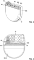
- Fig. 3 the elements of the implant are partially assembled.
- the electronic module 61 is placed on the energy storage device 62. Furthermore, the feedthrough 65 is connected to the electronic module 61.
- the energy storage device 62 (in the insulating sleeve 64) with the electronic module 61 is arranged in the second housing shell 60b.
- the first housing shell 60a is placed on the second housing shell 60b and the housing shells 60a, 60b are connected to one another, e.g. welded (not shown).
- the electrode connection device 63 is then placed on the housing 60 and connected to the feedthrough 65 (not shown).
- Fig. 4 shows a side view of an implant that is essentially the same as the implant
- the electronic module 61 is arranged in a support frame 69.
- the support frame 69 is arranged on the front side of the energy storage device 62.
- the support frame 69 serves to center the energy storage device 62 in the housing 60 and presses it against the housing base. This prevents the transmission of vibrations as well as pressure and tensile forces.
- the support frame 69 thus protects the components on the electronic module 61 as well as the electrical connection between the Energy storage device 62 and the electronic module 61 from destruction and/or loss of electrical contact.
- FIG. 5 A section of the electronic module 61 is shown in Fig. 5 shown (the lower part of Fig. 5 shows an enlarged detail of the upper part).
- the feedthrough 65 is formed as a multi-pole feedthrough with several pins 70. In the embodiment shown, five pins 70 are formed on the feedthrough 65, but a different number of pins is also possible. Each pin 70 is inserted into a pin receptacle 71 in order to form an electrical connection between the electronic module 61 and the electrode connection device 63 by means of the feedthrough 65.
- the first pin element 66a, 66b (e.g. anode and cathode of the battery) is formed on the energy storage device.
- the first pin receptacle 67a, 67b is arranged on the electronic module 61.
- the electronic module 61 is electrically connected to the energy storage device 62 by means of a straight plug connection by inserting the first pin element 66a, 66b into the first pin receptacle 67a, 67b.
- the connection can be designed as a redundant connection, for example by the first pin receptacle 67a, 67b comprising two pin receptacles arranged one above the other (two rings arranged one above the other) (not shown).
- the pins 70 of the feedthrough 65 and the first pin element 66a, 66b point in the same direction (contact direction), which determines the mounting direction for the elements.
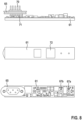
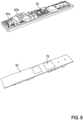
- An SMD component 72 is arranged on the back of the electronic module (cf. Fig. 8 and 9 ).
- Fig. 7 shows a block diagram of the implant.
- the functions of the electronic module are surrounded by the frame 80, which are implemented as units/chips on the electronic module and are explained in more detail below.
- a radio transceiver 81 is coupled to an antenna 82.
- the radio transceiver 81 is used for communication with an external device, in particular a programming device.
- an external device in particular a programming device.
- measured values and/or parameters of the implant can be transmitted to the programming device. Changed parameters for the implant can also be received from the programming device.
- the electronic module further comprises a control unit 83 (controller).
- the control unit 83 has a processor, e.g. a digital signal processor (DSP), a memory such as RAM (RAM - random-access memory) and/or ROM (ROM - read only memory) and a time unit (timer).
- DSP digital signal processor
- RAM random-access memory
- ROM read only memory
- timer time unit
- a memory access e.g. DMA (DMA - direct memory access) and/or network functions such as MAC (MAC - media access control) can be integrated into the control unit 83.
- DMA DMA - direct memory access
- MAC MAC - media access control
- a measuring unit 86 (sensing unit) is provided on the electronic module as a further component.
- the measuring unit 86 is configured to record measured values from the heart 91.
- a pacemaker unit 85 (pacing unit) is configured to generate stimulation pulses for the heart 91.
- the electronic module can optionally comprise a shock unit 84 (shocking unit) and an HV unit 87 (HV - high voltage), especially if the implant is designed as an ICD.
- the shock unit 84 is set up, the HV unit 87
- the HV unit 87 is configured to deliver a shock (defibrillation), for example with a voltage of 700 - 800 V.
- An EMC unit 88 (EMC - Electromagnetic Compatibility) is provided, which is designed to minimize or suppress the influence of electromagnetic fields.
- the electromagnetic fields can include interference radiation, the field of a shock delivered by the HV unit 87, the field of a stimulation pulse delivered by the pacemaker unit 85, the field of an external shock, the field of an external stimulation and fields from other external sources (e.g. a high frequency measurement).
- the EMC unit 88 is coupled to the housing 92 of the implant.
- the electronic module is coupled to a battery 90.
- An energy unit 89 of the electronic module comprises a switched-mode power supply (SMPS) and is configured for power management.
- SMPS switched-mode power supply
- the functions/units of the electronic module are implemented in various integrated circuits, i.e. in chips mounted on the electronic module.
- the dimensions of the chips are determined by their complexity of functions. The greater the complexity, the greater the planar extent of the chips.
- the size of the chips largely determines the size of the electronic module and also its orientation in the implant (parallel to the energy storage device). The size of the electronic module is also determined by the number of electrical connections between the chips, the chips with the non-integrated passive components and all other connections on the electronic module.
- Which therapy functions can be monolithically integrated on a chip using which manufacturing process or how many chips the electronic module contains depends on their operating voltage range, their data and signal complexity and their character, i.e. whether they have an analog, continuous-time or a digital, discrete-time or an analog-digital, mixed signal behavior.
- all of the functions listed above can be monolithically integrated, in particular the digital control functions, the analog-digital mixed sensing functions for ECG Signal amplification and evaluation (ECG - electrocardiogram), pacing for stimulation pulse generation, power management for optimal energy supply to the implant and shocking for voltage generation and control of the defibrillation shock.
- Manufacturing processes with the following characteristics are selected for manufacturing the integrated circuits on the electronic module: At least one chip is manufactured in a process with a minimum structure size F ⁇ 90 nm. Alternatively, at least one chip is manufactured in a process with a minimum structure size F ⁇ 65 nm. Alternatively, at least one chip is manufactured in a process with a minimum structure size F ⁇ 65 nm, on which a voltage of ⁇ 10 V can be switched simultaneously with respect to its substrate.
- At least one chip is manufactured in a process with a minimum structure size F ⁇ 65 nm, on which a voltage of ⁇ 10 V can be switched simultaneously with respect to its substrate and the SRAM memory functions (SRAM - static random-access memory, static RAM) of the chip have a capacity of ⁇ 3 megabits.
- ⁇ BGAs ball grid array packages
- PCB substrate printed circuit board substrate
- Solder balls are applied to the back of the substrate for SMD assembly.
- Packaging takes place in the panel.
- the printed circuit board substrate always has a uniform panel size for all chip sizes, which only depends on the mold tool of the transfer overmolding machine. Depending on the chip size, more or fewer chips fit on the panel, which are then sawn out of the panel in their final housing size after encapsulation and balling.
- a 205 mm x 70 mm panel has three square potting areas, each with an edge length of 56 mm, into which the chips are mounted and wire bonded (see Fig. Fig. 10A and 10B
- the application of this ⁇ TBGA packaging process to the electronic module leads to further features and extensions of the packaging process, which are described in the Fig. 10A to 10E
- the holes or fits of the cutting sleeves and/or clamping sleeves are drilled (see Fig. 10C ).
- the encapsulation not only serves to cover the chips, it is also part of the mechanical stability of the electronic module and in particular of the resulting plug connection.
- the panel is equipped with the SMD components of the electronic modules in the panel (see. Fig. 10D ).
- the edge lengths of the electronic module satisfy an integer division ratio of the potting surface edges of the panel minus the sawing losses.
- the components of the electronic module can be provided as ASICs (ASIC - application-specific integrated circuit).
- Fig. 11 shows an assembly 1 (also referred to as a header core) with a first receiving device 2 for an electrode plug and a second receiving device 13 for a further electrode plug.
- the first receiving device 2 has a front opening 6 through which the electrode plug can be inserted.
- the first receiving device 2 has a first section 3, a second section 4 and a third section 5.
- the diameter of the first section 3 is larger than the diameter of the second section 4.
- the diameter of the second section 4 is in turn larger than the diameter of the third section 5.
- the first receiving device 2 is gradually tapered from the front opening 6 to the end.
- a first connection element is formed between the first section 3 and the second section 4 (i.e. in a front area of the first receiving device 2).
- a second connection element 8 is formed between the second section 4 and the third section 5 (in a rear area of the first receiving device 2).
- Both the first connection element 7 and the second connection element 8 have at least two flat side surfaces. This enables the assembly 1 to be easily gripped during assembly and enables the assembly steps to be automated.
- the first connection element 7 and the second connection element 8 are essentially cuboid-shaped.
- the second connection element 8 has a bevelled edge 17, which serves to save material and to observe the flow direction of the epoxy resin.
- On a rear side of the first A recess 12a is formed in the plastic coating of the first connection element 7.
- a rear opening 12b is formed on a rear side of the second connection element 8.
- the assembly is partially surrounded by a plastic 11.
- the assembly is partially overmolded with polysulfone.
- Recesses for a first contact surface 9 and a second contact surface 10 are formed in the plastic 11.
- the first and second contact surfaces are formed as circular surfaces.
- a guide 16 is formed adjacent to the first and second contact surfaces 9, 10.
- the guide 16 serves to accommodate a connection element (e.g. a wiring strip).
- the guides on the contact surfaces prevent connection elements from different contact surfaces from touching one another.
- the second receiving device 13 is constructed analogously to the first receiving device 2. For reasons of clarity, the components of the second receiving device (an opening, the three step-shaped tapered sections and the two connection elements) are not provided with reference symbols.
- the second receiving device also has two contact surfaces (third contact surface 14 and fourth contact surface 15) for connections. Guides are again formed adjacent to the contact surfaces.
- a positioning device 18b is formed, which is designed as a pin with a tapered end.
- the pointed end of the positioning device 18b can be inserted into a receptacle in the housing to facilitate the precise positioning of the assembly on the housing.
- the assembly can also be designed without a positioning device 18b.
- Positioning pins 18a are formed on the underside of the assembly (cf. Fig. 12 ).
- the positioning pins can be placed in associated receptacles when arranging the assembly on the housing of the implant. In the embodiment shown, two positioning pins are shown, but other numbers of positioning pins are possible.
- the first receiving device 2 and the second receiving device 13 each have a spring sleeve and a plug receptacle.
- the first receiving device 2 and the second receiving device 13 can be designed as IS-1 connectors.
- a spring element 20 is arranged in the first receiving device 2 and fixed there (left side of Fig. 13 ).
- the recess 12a in the plastic is used to weld the spring element 20 arranged inside the first receiving device 2 into the first connection element 7 by means of resistance welding.
- another spring element is arranged and fastened in the second receiving device 13 (not shown).
- the openings of the assembly 1 are then closed and sealed with potting aids 21, 22, 23 (right side of Fig. 13 ).
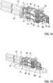
- FIG. 14 A further assembly step is shown.
- a wire band 24 is attached to the third contact surface 14 (e.g. welded).
- the wire band 24 has a wire band connection 25 which is connected to a pin contact of a feedthrough 30 (cf. Fig. 4 ) and can be plugged onto the pin contact, for example. Additional wire strips are connected to the other contact surfaces 9, 10, 15.
- An antenna 26 is attached to the assembly 1.
- the antenna 26 partially surrounds the first section 3 of the first receiving device 2 and is clipped to it.
- the antenna 26 has a U-shaped section 27. This forms a recessed grip that can be used, for example, with an automated gripper to hold and transport the assembly.
- An antenna connection 28 for connection to the feedthrough 30 is formed at a rear end of the antenna.
- the assembly with the wire bands and the antenna is then arranged in a mold (e.g. a silicone mold) (not shown).
- the wire band connections and the antenna connection 28 are plugged onto assigned pins of the feedthrough 30 and connected to the pins (e.g. welded).
- the mold is closed and filled with a synthetic resin 31 (e.g. epoxy resin). This forms the electrode connection device (see Fig. 16 ).
- the casting aids 21, 22, 23 are removed and any excess resin on the outer surfaces is removed, e.g. by grinding and/or polishing.
- the implant with the electrode connection device is now fully assembled ( Fig. 17 ).
- FIG. 18 A further embodiment of the implant is shown.
- the electrode connection device 53 is attached to a cover 121.
- the energy storage device 62 is accommodated in a housing 120.
- the housing 120 can be provided as a deep-drawn form.
- the cover 121 is welded to the housing 120 along a circumferential weld seam 122 in order to close the housing 120.
- a support frame 69 is arranged on the energy storage device.
- the support frame 69 accommodates the electronic module.
- the electrode connection device 53 can be made, for example, according to the Fig. 11 to 17 shown embodiment.
- the feedthrough 65 with the pins 70 is welded into the cover 121.
- the embodiments of the implant and methods disclosed herein may have the following advantages:
- the internal structure of the electronic implant is significantly simplified, so that manufacturing costs are reduced.
- the number and complexity of the required manufacturing processes is also reduced, so that the scalability of production is promoted (e.g. simplified transfer to other locations, low training requirements for employees, lower requirements for the required manufacturing environment and accompanying engineering).
- rework is possible or simplified when detachable connection techniques are used.
- the form factor of the electronic module allows the implant to be made smaller or the volume gained can be used to increase the battery capacity and thus extend the life of the implant.
- the production of the electronic module in ⁇ TBGA technology enables an increase in the benefit on the Panel and the associated manufacturing cost savings.
- the vertical mounting of the electronic module (parallel to the front of the energy storage device) enables electrical connections without angles and thus a simpler, more cost-effective construction of the implant optimized for automatic production in one axis.
Landscapes
- Health & Medical Sciences (AREA)
- Animal Behavior & Ethology (AREA)
- Biomedical Technology (AREA)
- Nuclear Medicine, Radiotherapy & Molecular Imaging (AREA)
- Radiology & Medical Imaging (AREA)
- Life Sciences & Earth Sciences (AREA)
- Engineering & Computer Science (AREA)
- General Health & Medical Sciences (AREA)
- Public Health (AREA)
- Veterinary Medicine (AREA)
- Electrotherapy Devices (AREA)
- Structures For Mounting Electric Components On Printed Circuit Boards (AREA)
- Prostheses (AREA)
- Non-Metallic Protective Coatings For Printed Circuits (AREA)
Applications Claiming Priority (3)
| Application Number | Priority Date | Filing Date | Title |
|---|---|---|---|
| EP18187090.8A EP3603740A1 (fr) | 2018-08-02 | 2018-08-02 | Implant |
| PCT/EP2019/069616 WO2020025366A1 (fr) | 2018-08-02 | 2019-07-22 | Implant |
| EP19748484.3A EP3829705B1 (fr) | 2018-08-02 | 2019-07-22 | Implant |
Related Parent Applications (2)
| Application Number | Title | Priority Date | Filing Date |
|---|---|---|---|
| EP19748484.3A Division-Into EP3829705B1 (fr) | 2018-08-02 | 2019-07-22 | Implant |
| EP19748484.3A Division EP3829705B1 (fr) | 2018-08-02 | 2019-07-22 | Implant |
Publications (2)
| Publication Number | Publication Date |
|---|---|
| EP4477257A2 true EP4477257A2 (fr) | 2024-12-18 |
| EP4477257A3 EP4477257A3 (fr) | 2024-12-25 |
Family
ID=63143086
Family Applications (3)
| Application Number | Title | Priority Date | Filing Date |
|---|---|---|---|
| EP18187090.8A Withdrawn EP3603740A1 (fr) | 2018-08-02 | 2018-08-02 | Implant |
| EP24209372.2A Pending EP4477257A3 (fr) | 2018-08-02 | 2019-07-22 | Implant |
| EP19748484.3A Active EP3829705B1 (fr) | 2018-08-02 | 2019-07-22 | Implant |
Family Applications Before (1)
| Application Number | Title | Priority Date | Filing Date |
|---|---|---|---|
| EP18187090.8A Withdrawn EP3603740A1 (fr) | 2018-08-02 | 2018-08-02 | Implant |
Family Applications After (1)
| Application Number | Title | Priority Date | Filing Date |
|---|---|---|---|
| EP19748484.3A Active EP3829705B1 (fr) | 2018-08-02 | 2019-07-22 | Implant |
Country Status (6)
| Country | Link |
|---|---|
| US (1) | US11672993B2 (fr) |
| EP (3) | EP3603740A1 (fr) |
| JP (2) | JP2021532902A (fr) |
| CN (1) | CN112533669A (fr) |
| SG (1) | SG11202100976YA (fr) |
| WO (1) | WO2020025366A1 (fr) |
Citations (5)
| Publication number | Priority date | Publication date | Assignee | Title |
|---|---|---|---|---|
| US7647110B2 (en) | 2002-04-30 | 2010-01-12 | St. Jude Medical Ab | Modular implantable medical device and manufacturing method therefor |
| EP2493557B1 (fr) | 2009-10-30 | 2017-05-17 | Medtronic, Inc. | Embases de dispositifs médicaux implantables facilitant des variantes dans la configuration des dispositifs et des dérivations |
| US9713717B2 (en) | 2013-12-09 | 2017-07-25 | Boston Scientific Neuromodulation Corporation | Implantable stimulator device having components embedded in a circuit board |
| US9737721B2 (en) | 2013-09-05 | 2017-08-22 | Boston Scientific Neuromodulation Corporation | Construction for an implantable medical device having a battery affixed to the case |
| US20180054034A1 (en) | 2009-10-30 | 2018-02-22 | Medtronic, Inc. | Implantable medical devices including elongated conductor bodies that facilitate device and lead configuration variants |
Family Cites Families (14)
| Publication number | Priority date | Publication date | Assignee | Title |
|---|---|---|---|---|
| US5144946A (en) * | 1991-08-05 | 1992-09-08 | Siemens Pacesetter, Inc. | Combined pacemaker substrate and electrical interconnect and method of assembly |
| US6567703B1 (en) * | 2000-11-08 | 2003-05-20 | Medtronic, Inc. | Implantable medical device incorporating miniaturized circuit module |
| ATE460753T1 (de) * | 2001-07-19 | 2010-03-15 | Greatbatch Ltd | Gewölbtes gehäuse für eine implantierbare medizinische vorrichtung |
| US7437193B2 (en) * | 2002-06-28 | 2008-10-14 | Boston Scientific Neuromodulation Corporation | Microstimulator employing improved recharging reporting and telemetry techniques |
| EP2329860B1 (fr) * | 2009-12-03 | 2015-09-02 | Biotronik CRM Patent AG | Boîtier de raccordement et sa fabrication |
| CN102397625A (zh) * | 2010-09-15 | 2012-04-04 | 鼎迈医疗科技(苏州)有限公司 | 植入式有源电子装置及电刺激系统 |
| EP2535926A3 (fr) * | 2011-06-17 | 2015-08-05 | BIOTRONIK SE & Co. KG | Conditionnement de semi-conducteur |
| US8649869B2 (en) * | 2012-03-05 | 2014-02-11 | Pacesetter, Inc. | Implantable medical device having feedthru assembly with header side bunched conductor array and can side linear conductor array |
| US8843215B2 (en) * | 2012-06-13 | 2014-09-23 | Biotronik Se & Co. Kg | Connecting device |
| US10431345B2 (en) * | 2014-06-13 | 2019-10-01 | City Labs, Inc. | Small form factor betavoltaic battery for use in applications requiring a volumetrically-small power source |
| AU2014315492B2 (en) * | 2013-09-05 | 2017-04-20 | Boston Scientific Neuromodulation Corporation | Construction for an implantable medical device having a battery affixed to the case |
| AU2014315486B2 (en) * | 2013-09-05 | 2016-12-22 | Boston Scientific Neuromodulation Corporation | Construction for an implantable medical device employing an internal support structure |
| US9992866B2 (en) * | 2015-03-31 | 2018-06-05 | Biotronik Se & Co. Kg | Printed circuit board arrangement and electronic device having a printed circuit board device |
| CN110234392B (zh) * | 2017-01-26 | 2023-08-11 | 心脏起搏器股份公司 | 具有被包覆模制的组件的无引线装置 |
-
2018
- 2018-08-02 EP EP18187090.8A patent/EP3603740A1/fr not_active Withdrawn
-
2019
- 2019-07-22 JP JP2021505725A patent/JP2021532902A/ja active Pending
- 2019-07-22 EP EP24209372.2A patent/EP4477257A3/fr active Pending
- 2019-07-22 CN CN201980051641.0A patent/CN112533669A/zh active Pending
- 2019-07-22 WO PCT/EP2019/069616 patent/WO2020025366A1/fr not_active Ceased
- 2019-07-22 EP EP19748484.3A patent/EP3829705B1/fr active Active
- 2019-07-22 SG SG11202100976YA patent/SG11202100976YA/en unknown
- 2019-07-22 US US17/264,022 patent/US11672993B2/en active Active
-
2024
- 2024-04-08 JP JP2024062231A patent/JP2024086816A/ja active Pending
Patent Citations (5)
| Publication number | Priority date | Publication date | Assignee | Title |
|---|---|---|---|---|
| US7647110B2 (en) | 2002-04-30 | 2010-01-12 | St. Jude Medical Ab | Modular implantable medical device and manufacturing method therefor |
| EP2493557B1 (fr) | 2009-10-30 | 2017-05-17 | Medtronic, Inc. | Embases de dispositifs médicaux implantables facilitant des variantes dans la configuration des dispositifs et des dérivations |
| US20180054034A1 (en) | 2009-10-30 | 2018-02-22 | Medtronic, Inc. | Implantable medical devices including elongated conductor bodies that facilitate device and lead configuration variants |
| US9737721B2 (en) | 2013-09-05 | 2017-08-22 | Boston Scientific Neuromodulation Corporation | Construction for an implantable medical device having a battery affixed to the case |
| US9713717B2 (en) | 2013-12-09 | 2017-07-25 | Boston Scientific Neuromodulation Corporation | Implantable stimulator device having components embedded in a circuit board |
Also Published As
| Publication number | Publication date |
|---|---|
| EP3829705A1 (fr) | 2021-06-09 |
| WO2020025366A1 (fr) | 2020-02-06 |
| US11672993B2 (en) | 2023-06-13 |
| JP2024086816A (ja) | 2024-06-28 |
| EP3829705B1 (fr) | 2024-12-04 |
| EP3603740A1 (fr) | 2020-02-05 |
| EP4477257A3 (fr) | 2024-12-25 |
| US20210316147A1 (en) | 2021-10-14 |
| JP2021532902A (ja) | 2021-12-02 |
| SG11202100976YA (en) | 2021-03-30 |
| CN112533669A (zh) | 2021-03-19 |
Similar Documents
| Publication | Publication Date | Title |
|---|---|---|
| EP3829702B1 (fr) | Implant et procédé de montage d'un implant | |
| EP2111895B1 (fr) | Boîtier de connexion pour un implant électromédical | |
| DE69930785T2 (de) | Festelektrolytkondensator in Chip-Bauweise und dessen Herstellungsverfahren | |
| EP2329860B1 (fr) | Boîtier de raccordement et sa fabrication | |
| DE19640304C2 (de) | Chipmodul insbesondere zur Implantation in einen Chipkartenkörper | |
| EP3829705B1 (fr) | Implant | |
| EP3829703A1 (fr) | Implant et procédé de production d'un implant | |
| EP1407801B1 (fr) | Implant électromédical pour le traitement intracardiaque du coeur | |
| DE202007018766U1 (de) | Kontaktmodul für ein medizinisches Implantat | |
| EP3829704A1 (fr) | Implant et procédé de réalisation d'une connexion électrique entre un module électronique et un composant électronique d'un implant | |
| EP3603744B1 (fr) | Module pour une tête, tête et implant pourvu de la tête ainsi que procédé de montage d'une tête | |
| EP1832311A2 (fr) | Générateur d'impulsions implantable |
Legal Events
| Date | Code | Title | Description |
|---|---|---|---|
| PUAI | Public reference made under article 153(3) epc to a published international application that has entered the european phase |
Free format text: ORIGINAL CODE: 0009012 |
|
| STAA | Information on the status of an ep patent application or granted ep patent |
Free format text: STATUS: THE APPLICATION HAS BEEN PUBLISHED |
|
| PUAL | Search report despatched |
Free format text: ORIGINAL CODE: 0009013 |
|
| AC | Divisional application: reference to earlier application |
Ref document number: 3829705 Country of ref document: EP Kind code of ref document: P |
|
| AK | Designated contracting states |
Kind code of ref document: A2 Designated state(s): AL AT BE BG CH CY CZ DE DK EE ES FI FR GB GR HR HU IE IS IT LI LT LU LV MC MK MT NL NO PL PT RO RS SE SI SK SM TR |
|
| AK | Designated contracting states |
Kind code of ref document: A3 Designated state(s): AL AT BE BG CH CY CZ DE DK EE ES FI FR GB GR HR HU IE IS IT LI LT LU LV MC MK MT NL NO PL PT RO RS SE SI SK SM TR |
|
| RIC1 | Information provided on ipc code assigned before grant |
Ipc: A61N 1/378 20060101ALI20241120BHEP Ipc: A61N 1/375 20060101AFI20241120BHEP |
|
| STAA | Information on the status of an ep patent application or granted ep patent |
Free format text: STATUS: REQUEST FOR EXAMINATION WAS MADE |
|
| 17P | Request for examination filed |
Effective date: 20250617 |
|
| STAA | Information on the status of an ep patent application or granted ep patent |
Free format text: STATUS: EXAMINATION IS IN PROGRESS |
|
| 17Q | First examination report despatched |
Effective date: 20250829 |