EP4483799A1 - Système et procédé de détection de la position et de la force d'un cathéter - Google Patents
Système et procédé de détection de la position et de la force d'un cathéter Download PDFInfo
- Publication number
- EP4483799A1 EP4483799A1 EP24184690.6A EP24184690A EP4483799A1 EP 4483799 A1 EP4483799 A1 EP 4483799A1 EP 24184690 A EP24184690 A EP 24184690A EP 4483799 A1 EP4483799 A1 EP 4483799A1
- Authority
- EP
- European Patent Office
- Prior art keywords
- smd
- coils
- fcb
- orientation
- magnetic
- Prior art date
- Legal status (The legal status is an assumption and is not a legal conclusion. Google has not performed a legal analysis and makes no representation as to the accuracy of the status listed.)
- Pending
Links
Images


Classifications
-
- A—HUMAN NECESSITIES
- A61—MEDICAL OR VETERINARY SCIENCE; HYGIENE
- A61B—DIAGNOSIS; SURGERY; IDENTIFICATION
- A61B5/00—Measuring for diagnostic purposes; Identification of persons
- A61B5/06—Devices, other than using radiation, for detecting or locating foreign bodies ; Determining position of diagnostic devices within or on the body of the patient
- A61B5/061—Determining position of a probe within the body employing means separate from the probe, e.g. sensing internal probe position employing impedance electrodes on the surface of the body
- A61B5/062—Determining position of a probe within the body employing means separate from the probe, e.g. sensing internal probe position employing impedance electrodes on the surface of the body using magnetic field
-
- A—HUMAN NECESSITIES
- A61—MEDICAL OR VETERINARY SCIENCE; HYGIENE
- A61M—DEVICES FOR INTRODUCING MEDIA INTO, OR ONTO, THE BODY; DEVICES FOR TRANSDUCING BODY MEDIA OR FOR TAKING MEDIA FROM THE BODY; DEVICES FOR PRODUCING OR ENDING SLEEP OR STUPOR
- A61M25/00—Catheters; Hollow probes
- A61M25/01—Introducing, guiding, advancing, emplacing or holding catheters
- A61M25/0105—Steering means as part of the catheter or advancing means; Markers for positioning
-
- A—HUMAN NECESSITIES
- A61—MEDICAL OR VETERINARY SCIENCE; HYGIENE
- A61B—DIAGNOSIS; SURGERY; IDENTIFICATION
- A61B5/00—Measuring for diagnostic purposes; Identification of persons
- A61B5/06—Devices, other than using radiation, for detecting or locating foreign bodies ; Determining position of diagnostic devices within or on the body of the patient
- A61B5/065—Determining position of the probe employing exclusively positioning means located on or in the probe, e.g. using position sensors arranged on the probe
-
- A—HUMAN NECESSITIES
- A61—MEDICAL OR VETERINARY SCIENCE; HYGIENE
- A61B—DIAGNOSIS; SURGERY; IDENTIFICATION
- A61B34/00—Computer-aided surgery; Manipulators or robots specially adapted for use in surgery
- A61B34/20—Surgical navigation systems; Devices for tracking or guiding surgical instruments, e.g. for frameless stereotaxis
-
- A—HUMAN NECESSITIES
- A61—MEDICAL OR VETERINARY SCIENCE; HYGIENE
- A61B—DIAGNOSIS; SURGERY; IDENTIFICATION
- A61B5/00—Measuring for diagnostic purposes; Identification of persons
- A61B5/68—Arrangements of detecting, measuring or recording means, e.g. sensors, in relation to patient
- A61B5/6846—Arrangements of detecting, measuring or recording means, e.g. sensors, in relation to patient specially adapted to be brought in contact with an internal body part, i.e. invasive
- A61B5/6847—Arrangements of detecting, measuring or recording means, e.g. sensors, in relation to patient specially adapted to be brought in contact with an internal body part, i.e. invasive mounted on an invasive device
- A61B5/6852—Catheters
-
- G—PHYSICS
- G01—MEASURING; TESTING
- G01B—MEASURING LENGTH, THICKNESS OR SIMILAR LINEAR DIMENSIONS; MEASURING ANGLES; MEASURING AREAS; MEASURING IRREGULARITIES OF SURFACES OR CONTOURS
- G01B7/00—Measuring arrangements characterised by the use of electric or magnetic techniques
- G01B7/003—Measuring arrangements characterised by the use of electric or magnetic techniques for measuring position, not involving coordinate determination
-
- G—PHYSICS
- G01—MEASURING; TESTING
- G01L—MEASURING FORCE, STRESS, TORQUE, WORK, MECHANICAL POWER, MECHANICAL EFFICIENCY, OR FLUID PRESSURE
- G01L1/00—Measuring force or stress, in general
- G01L1/12—Measuring force or stress, in general by measuring variations in the magnetic properties of materials resulting from the application of stress
- G01L1/127—Measuring force or stress, in general by measuring variations in the magnetic properties of materials resulting from the application of stress by using inductive means
-
- G—PHYSICS
- G01—MEASURING; TESTING
- G01R—MEASURING ELECTRIC VARIABLES; MEASURING MAGNETIC VARIABLES
- G01R33/00—Arrangements or instruments for measuring magnetic variables
- G01R33/0005—Geometrical arrangement of magnetic sensor elements; Apparatus combining different magnetic sensor types
-
- G—PHYSICS
- G01—MEASURING; TESTING
- G01R—MEASURING ELECTRIC VARIABLES; MEASURING MAGNETIC VARIABLES
- G01R33/00—Arrangements or instruments for measuring magnetic variables
- G01R33/0052—Manufacturing aspects; Manufacturing of single devices, i.e. of semiconductor magnetic sensor chips
-
- G—PHYSICS
- G01—MEASURING; TESTING
- G01R—MEASURING ELECTRIC VARIABLES; MEASURING MAGNETIC VARIABLES
- G01R33/00—Arrangements or instruments for measuring magnetic variables
- G01R33/02—Measuring direction or magnitude of magnetic fields or magnetic flux
- G01R33/0206—Three-component magnetometers
-
- G—PHYSICS
- G01—MEASURING; TESTING
- G01R—MEASURING ELECTRIC VARIABLES; MEASURING MAGNETIC VARIABLES
- G01R33/00—Arrangements or instruments for measuring magnetic variables
- G01R33/02—Measuring direction or magnitude of magnetic fields or magnetic flux
- G01R33/028—Electrodynamic magnetometers
-
- H—ELECTRICITY
- H05—ELECTRIC TECHNIQUES NOT OTHERWISE PROVIDED FOR
- H05K—PRINTED CIRCUITS; CASINGS OR CONSTRUCTIONAL DETAILS OF ELECTRIC APPARATUS; MANUFACTURE OF ASSEMBLAGES OF ELECTRICAL COMPONENTS
- H05K1/00—Printed circuits
- H05K1/18—Printed circuits structurally associated with non-printed electric components
- H05K1/189—Printed circuits structurally associated with non-printed electric components characterised by the use of flexible or folded printed circuits
-
- A—HUMAN NECESSITIES
- A61—MEDICAL OR VETERINARY SCIENCE; HYGIENE
- A61B—DIAGNOSIS; SURGERY; IDENTIFICATION
- A61B34/00—Computer-aided surgery; Manipulators or robots specially adapted for use in surgery
- A61B34/20—Surgical navigation systems; Devices for tracking or guiding surgical instruments, e.g. for frameless stereotaxis
- A61B2034/2046—Tracking techniques
- A61B2034/2051—Electromagnetic tracking systems
-
- A—HUMAN NECESSITIES
- A61—MEDICAL OR VETERINARY SCIENCE; HYGIENE
- A61B—DIAGNOSIS; SURGERY; IDENTIFICATION
- A61B2562/00—Details of sensors; Constructional details of sensor housings or probes; Accessories for sensors
- A61B2562/12—Manufacturing methods specially adapted for producing sensors for in-vivo measurements
-
- A—HUMAN NECESSITIES
- A61—MEDICAL OR VETERINARY SCIENCE; HYGIENE
- A61M—DEVICES FOR INTRODUCING MEDIA INTO, OR ONTO, THE BODY; DEVICES FOR TRANSDUCING BODY MEDIA OR FOR TAKING MEDIA FROM THE BODY; DEVICES FOR PRODUCING OR ENDING SLEEP OR STUPOR
- A61M25/00—Catheters; Hollow probes
- A61M25/01—Introducing, guiding, advancing, emplacing or holding catheters
- A61M25/0105—Steering means as part of the catheter or advancing means; Markers for positioning
- A61M2025/0166—Sensors, electrodes or the like for guiding the catheter to a target zone, e.g. image guided or magnetically guided
Definitions
- the present invention is in the field of catheters and particularly relates to systems and methods for sensing catheter's location and the force applied thereby.
- a catheter/probe In various therapeutic and diagnostic procedures, a catheter/probe is inserted into a patient's body (e.g., chamber of the heart) and to be brought into contact with a body tissue there. Typically, in such procedures, it is necessary to determine the catheter's location within the body (i.e., the location at which a distal tip of the catheter engages the body tissue) as well as the pressure applied thereby to the tissue.
- Catheters having integrated location and pressure sensors for sensing the location of the catheter and the pressure/force applied thereby at the contact region with the tissue are generally known. Such catheters typically utilize inductive coils for determining the location of the catheter within the body and/or the pressure/force applied thereby to a body tissue it engages with.
- U.S. patent No. U.S.8,535,308 and U.S. patent application No. U.S. 2020/015693 which are both assigned to the assignee of the present Application, disclose for example configurations of such catheters utilizing sensory circuits having several coils, for sensing the location and orientation of the catheter body, as well as the force applied thereby at the interface with the tissue.
- the present invention achieves that by providing a novel position sensor, which is particularly suited for furnishing sensor coils of high impedance (high induced-voltage) within the narrow dimensions of a catheter body.
- a position sensor adapted to measure signals indicative of at least one of a location and orientation of the sensor relative to one or more magnetic fields.
- the position sensor includes a circuit board, and at least three coils located on the circuit board and arranged for sensing different aspects of the magnetic field, which are indicative of at least one of a location and orientation of the sensor relative to the external magnetic field.
- the circuit board is a flexible circuit board (FCB) and the at least three coils are at least three surface mount coil devices (SMD coils) mounted on the FCB via surface mount technology (SMT).
- the FCB is furnished at the sensor in folded/rolled state such that the magnetic flux axes of at least three of the SMD coils mounted on its surface are not co-planar to thereby enable to utilize signals obtained from the at least three SMD coils for measuring at least one of the orientation and location of the sensor relative to one or more magnetic field sources.
- the positioning sensor is adapted to measure signals indicative of an orientation of the sensor relative to a first magnetic field source located in-front of the position sensor (e.g. in- front with respect to a longitudinal axis thereof being an axis about which the FCB is folded).
- the at least three SMD coils include three SMD coils arranged on the FCB such that their magnetic flux axes are parallel to one another and are not co-planar when the FCB is furnished at the sensor in the folded/rolled state. This thereby enable to utilize signals obtained from the three SMD coils to determine two angles of orientation of the relative the first magnetic field source being located in-front of the three SMD coils along a general direction of their magnetic flux axes.
- the three SMD coils are surface mounted to the surface of the FCB via surface mount technology such that their magnetic flux axes are oriented parallel relative to the surface of the FCB at which they are mounted.
- the FCB is arranged in folded/rolled form at the sensor such that a folding/rolling axis of folded/rolled form of the FCB is substantially parallel to the parallel magnetic flux axes of the three SMD coils thereon.
- the position sensor is adapted to measure signals indicative of location and orientation of the sensor relative to one or more second magnetic field sources.
- the at least three SMD coils include three SMD coils arranged on the FCB such that when the FCB is folded at the sensor, the magnetic flux axes of the three SMD coils span three dimensional (3D) coordinates. This thereby enables to utilize signals obtained from the three SMD coils to determine a location and an orientation of the sensor relative the one or more magnetic field sources.
- two SMD coils of the at least three SMD coils of the position sensor are surface mounted to the surface of the FCB via surface mount technology and located on the FCB with vertical orientation of their magnetic flux axes relative to the FCB surface.
- a third SMD coil of the at least three SMD coils is surface mounted to the surface of the FCB via surface mount technology with parallel orientation of its magnetic flux axis relative to the FCB surface. This thereby enables to utilize signals obtained from the three SMD coils in order to determine a location and orientation of the sensor relative to the one or more external magnetic field sources.
- the position sensor includes at least five SMD coils surface mounted to one or more FCBs of the sensor.
- a first subset of three SMD coils of the at least five SMD coils are arranged such that their magnetic flux axes are parallel to one another and are not co-planar when the FCB is furnished at the sensor in folded/rolled state to thereby enable utilization of the signals obtained thereby to determine two angles of orientation of the sensor relative to the first magnetic field source located in-front of these three SMD coils along a general direction of their magnetic flux axes.
- a second subset of three SMD coils of the at least five SMD coils are arranged such that when the FCB is furnished at the sensor in folded/rolled state, the magnetic flux axes thereof span 3D coordinates. This thereby enables utilization of the signals obtained from the three SMD coils of the second subset to determine a location and orientation of the sensor relative one or more second magnetic field sources.
- At least one SMD coil of the at least three SMD coils of the sensor includes a coil portion and at least one surface mount portion arranged from at least one respective side of the coil portion.
- the coil portion includes a ferrite core and a conductive winding arrangement arranged in a helix directly over an external surface of the ferrite core with a pitch of the helix not exceeding 13 ⁇ m and in some embodiments not exceeding 12 ⁇ m to thereby provide that the SMD-Coil has compact dimensions and high impedance.
- the ferrite core may for instance include material of relative magnetic permeability ⁇ r in the order of at least 100 which is stable with tolerance of ⁇ 0.3 % within a temperature range between about 20°C to 60°C. This thereby enables consistent magnetic field measurements during operation under variable temperature conditions within said temperature range.
- the conductive winding arrangement are fabricated directly over the external surface of the ferrite core, utilizing photolithography.
- At least one SMD coil of the at least three SMD coils is mounted on the FCB with a flat/parallel orientation of its magnetic flux axis relative to the FCB surface.
- the at least one SMD coil includes a coil portion having a conductive winding arrangement, and at least two SMT-mounting portions arranged from opposite sides of the coil portion and having at least two respective electric contacts electrically coupled to the FCB with SMT electrical connection, and respectively electrically connected to opposite ends of the conductive winding arrangement.
- At least one SMD coil of the at least three SMD coils is mounted in a vertical/perpendicular orientation of its magnetic flux axis relative to the FCB surface.
- the at least one SMD coil includes a coil portion having a conductive winding arrangement and at least one SMT-mounting portion arranged from at least one side of the coil portion and having at least two electric contacts electrically coupled to the FCB via SMT electrical connection and respectively electrically connected to opposite ends of the conductive winding arrangement.
- the medical instrument is a catheter having an elongated housing including a main section having a longitudinal axis, and a tip section flexibly coupled at a distal end of the main section and including the first magnetic field source.
- the position sensor is accommodated at the main section of the elongated housing such that said FCB being folded/rolled about an axis parallel to the longitudinal axis of the catheter.
- the first subset of coils of the sensor facilitates determining an orientation of the tip section relative to the main section of the housing based on measurement of magnetic fields from the first magnetic field source that is located at the tip section.
- the second subset of coils of the sensor facilitates determining a location and an orientation of the main section relative to the one or more external second magnetic field sources (which may be located externally to the medical instrument).
- the medical instrument is a catheter having a body of tubular shape with characteristic inner diameter of about 2.5 millimeters or less.
- the folding is carried out such that a diameter of the FCB after being folded is smaller than the characteristic inner diameter of the body of the catheter; and the method includes placing the folded FCB within said body.
- the magnetic position sensor is adapted to measure signals indicative of an orientation of the sensor relative to a magnetic field source.
- the mounting of the at least three SMD coils includes mounting three of the SMD coils on the FCB such that their magnetic flux axes are parallel to one another and are not co-planar when the FCB is folded to the tubular form, to thereby enable to utilizing signals obtained from these three SMD coils to determine two angles of orientation of the relative a magnetic field source located in-front of the three SMD coils along a general direction of their magnetic flux axes.
- the magnetic position sensor is adapted to measure signals indicative of an orientation of the sensor relative a first magnetic field source and signals indicative of location and orientation of the sensor relative to one or more second external magnetic field sources.
- the at least three SMD coils include at least five SMD, and the mounting includes mounting the at least five SMD coils such that the following arrangement of magnetic flux axes thereof is obtained when the FCB is folded into to the tubular form:
- the providing of the at least three SMD coils includes fabricating at least one SMD coil of the SMD coils utilizing a photolithographic method of the present invention and thereby forming helical windings directly on a ferrite core of the coil.
- the photolithographic method includes for example:
- SMD-Coils surface mounted coils devices
- desired traits for such SMD-Coils include inter-alia high density helical windings closely packed over a tubular high permeability and electrically insulating magnetic core, and more specifically high-count helical windings/turns per unit length of the tubular magnetic core and per winding layer thereover.
- lithography-based coil fabrication methods of the present invention is a high-density winding with winding count in the order of at least 100 to 150 turns per millimeter of core length (e.g., per winding layer) directly over a magnetic core.
- wire-winding coil fabrication techniques of the present invention facilitate high-density winding with multiple winding layers and with winding count in the order of about 80 turns per layer per millimeter of core length (e.g., 77-83 turns per layer per millimeter), directly over the core.
- the coil fabrication techniques of the invention facilitate the fabrication of the windings over high-permeability (and electrically insulating) tubular magnetic core with relative permeability in the order of hundreds or more (e.g., relative permeability ⁇ r of at least 100).
- tubular is used herein to generally designate a body having a longitudinal axis of symmetry for discrete set or continuous set of rotations (i.e., generally any shape, such as cylindrical or conic shape having a longitudinal axis of symmetry, e.g., along its z axis, and lateral cross-section in the x-y plane, which may be smooth, e.g., circular or elliptic, or polygonal, e.g., triangle, rectangle etc.).
- aspects of the present invention particularly pertain to Helical SMD-coils having tubular magnetic cores, with one or more helical conductive windings arranged over the tubular magnetic core (in case of a plurality of helical conductive windings, the plurality of helical windings may be connected in series or parallel and may be arranged concentrically about the core).
- the helical conductive windings may have elliptic, circular, polygonal cross-sectional shape, which typically follows the core's cross-section.
- the helical SMD-coils of the invention may be fabricated with smaller size and/or smaller cross-section as compared to planar coils as planar concentric coils (in which magnetic core, if exists, lays below the planar coil). More over the helical SMD-coils of various embodiments of the invention are designed for Surface Mount assembly on electronic circuitry, thus enabling more efficient, fast reliable and cost-effective assembly of the coils on sensor circuits.
- the compact helical SMD-coils are fabricated with the windings formed/wrapped over the magnetic core (differently from some conventional techniques of compact high winding count coil fabrication which require an additional post-winding (manual) step of inserting the core within the windings). This also in turn facilitates a more cost-effective fabrication process of compact coils with uniform production yield.
- magnetic core as well as the terms ferrite and ferrite core, which are used herein interchangeably, are used herein to designate a bulk/body of magnetic material/composition or mixture, with relative permeability ⁇ r >>1.
- substantially pure magnetic material and pure ferrite are used herein to designate a bulk/body of material which has relative permeability ⁇ r >>1 and which is substantially not mixed/compound with other materials.
- magnetic material suited for the SMD-Coils of the present invention are typically of a type having magnetic properties of a so called soft-ferrite (i.e., having relatively low coercivity making it suitable for use in electrical applications such as inductors).
- Cores of substantially pure magnetic materials are typically sintered to form a solid structure, yet the sintered structure remains relatively physically weak/brittle and easily damageable during fabrication processes.
- a bulk of pure soft magnetic material / core may be susceptible to structurally damage (fractured/breakage) under the pressure applied thereto during physical wire winding process.
- the surface composition and crystalline structure of ferrite core e.g. of substantially pure/unmixed magnetic material
- may be relatively easily damaged when exposed to high intensity light for example when using a laser to ablate copper from the ferrite surface, which may generate surface temperature greater than 1000C, leading to conversion of the material conductivity properties e.g.
- the conventional techniques for fabrication of helical surface-mountable coils are limited and less suited for fabrication of compact helical SMD-coils having high density of windings over a magnetic-core of highly permeable (e.g., substantially pure) magnetic materials (particularly over a " soft " magnetic-core), and are also associated with high costs for fabrication of such coils and with non-uniform production yield.
- the present invention provides novel and inventive Helical SMD coil fabrication techniques and novel and inventive Helical SMD coil configurations facilitating to overcome some or all of the above deficiencies of the conventional techniques, that enable substantially automated fabrication of compact Helical SMD coils having high winding density (with wire-winding pitch down to a few microns) over highly permeable magnetic materials while alleviating some of the geometrical restrictions imposed by the conventional techniques on fabrication of such coils (such as limitation on the permissible aspect ratio), while advantageously yielding a more uniform production yield.
- a surface mounted coil device (SMD-Coil).
- the SMD-Coil includes a coil portion having a ferrite core; and conductive winding arrangement which includes a conductor arranged in a helix that circumferences the ferrite core about a longitudinal axis thereof.
- the SMD-Coil also includes at least one surface mount portion, arranged from at least one respective side of the coil portion, and having at least one electric contact coupler for electrically coupling the conductive winding arrangement of the coil portion to a circuit via surface mount technology (SMT).
- SMT surface mount technology
- the continuous conductor of the conductive winding arrangement is winded directly over an external surface layer of the ferrite core whereby a pitch of conductive windings in the helical conductive winding arrangement does not exceed 12 or 13 ⁇ m. Accordingly, the SMD-Coil is obtained with compact dimensions and high impedance (yielding high magnetic field induced voltage) which is particularly suitable for SMT installment in magnetic field sensors.
- the SMD-Coil is configured for flat/parallel installation on a surface of a circuit.
- at least two SMT-mounting portions are arranged from opposite sides of the coil portion and each of them includes at least one electric contact electrically connected to the conductive winding arrangement from a respective end thereof.
- the SMT-mounting portions with said electric contacts are therefore suitable for SMT installation on a circuit board such that the SMD-coil is mountable to the circuit board surface with its magnetic flux axis substantially parallel to the surface of the circuit board.
- the SMD-coil is configured for vertical/perpendicular installation on the surface of a circuit board.
- the at least one SMT-mounting portion may be a single SMT-mounting portion including at least two electric contacts respectively electrically connected near about opposite ends of the conductive winding arrangement and suitable for the SMT installation on the circuit board.
- the SMD-coil is thereby mountable to the surface of a circuit board surface with its magnetic flux axis substantially perpendicular to the circuit's surface.
- the ferrite core of the SMD-Coil includes material of relative magnetic permeability ⁇ r in the order of at least 100 and the relative magnetic permeability of the ferrite core material is stable (with tolerance of ⁇ 0.3 %) within a temperature range between about 20°C to 60°C. This thereby enables consistent magnetic field measurements during operation under variable temperature conditions within said temperature range.
- a method for fabricating a helical coil directly on a ferrite core such that its circumferences the ferrite core includes:
- the method is adapted for fabrication of the conductive helical coil with high density windings, whereby a pitch of the helical pattern and correspondingly of the conductive helical coil is in the order of, or less than 10 ⁇ m (and even down to 8 ⁇ m ) .
- the ferrite core includes, or is constituted by, fully sintered magnetic material having relative magnetic permeability ⁇ r in the order of at least 100.
- the above indicated photolithography operation may utilizes a photolithographic light source providing light power density (LPD) and wavelength suited for patterning the photoresists while not inducing substantial damage to the ferrite core.
- LPD light power density
- the application of the photoresist layer includes applying a layer of dry photoresist with thickness of at least 8 ⁇ m. This thereby enables the electroplating operation to yield narrow line width of the helical conductive coil with small pitch between adjacent lines while preventing spread of the electroplating between the lines.
- the method further includes fabrication of a seed layer over at least a section of the ferrite core in order to increase a surface conductivity of the ferrite to facilitate the electroplating. Additionally, or alternatively, in some implementation of the method, after the electroplating, remaining photoresists material is removed from between conductive windings of the helical coil.
- the method is adapted to fabricate further elements of the surface mounted coil device (SMD-Coil).
- the method may further include one or more of the following:
- the method is adapted for fabrication of a surface mounted coil device (SMD-Coil) suitable for flat/parallel installment on a circuit surface.
- the ferrite core may be provided with at least two surface mount portions, arranged from at least two respective side thereof. Accordingly, operations (b.) to (d.) may be applied to form respective conductive couplings between two designated locations at the respective surface mount portions and corresponding ends of said conductive helical coil. This thereby enables flat/parallel installment of the SMD-Coil on a surface of a circuit board, with the two designated locations at the two surface mount portions respectively providing electric contacts between circuit and respective ends of the conductive helical coil.
- the method is adapted for fabrication of a surface mounted coil device (SMD-Coil) which is adapted vertical/perpendicular installment on a surface of a circuit board.
- the ferrite core may be provided in this case with at least one/single surface mount portion arranged from one side thereof.
- the ferrite core may in this case also include a conductive bulk path that passes through a bulk of the ferrite core from an electric contact of the surface mount portion located at said one respective side, towards an opposite side of the ferrite core at which a conductive region of the conductive path is exposed. Accordingly in such embodiments the operations (b.) to (d.) of the method may be applied to form:
- a method for fabricating a surface mounted coil device having a helical coil directly on a ferrite core and to circumference the ferrite core includes:
- the ferrite core is comprises fully sintered magnetic material (i.e., with no non-magnetic structurally enforcing additives) thereby providing relative magnetic permeability ⁇ r in the order of at least 100 or higher.
- a surface mounted coil device including a coil portion having a ferrite core and a conductive winding arrangement.
- the conductive winding arrangement includes a conductor arranged in a helix that circumferences the ferrite core about a longitudinal axis thereof.
- the SMD-Coil also includes at least one surface mount portion, arranged from at least one respective side of the coil portion, and having at least one electric contact coupler for electrically coupling the conductive winding arrangement of the coil portion to a circuit via surface mount technology (SMT).
- SMT surface mount technology
- the SMD-Coil is fabricated according to any one of the methods of the present invention described above such that the continuous conductor of the conductive winding arrangement is winded/arranged directly over an external surface layer of the ferrite core with a pitch of the helix of the conductive winding arrangement not exceeding 13 ⁇ m and in some cases not exceeding 12 ⁇ m.
- the SMD-Coil 10 generally includes a Coil Portion C having a core FC of magnetic material (also referred to herein interchangeable as Ferrite Core) and a conductive winding arrangement CW, which includes a conductor which is arranged in a helix that is winded around the magnetic core FC about a longitudinal axis FX thereof.
- FC magnetic material
- CW conductive winding arrangement
- the SMD-Coil 10 also includes one or more Surface Mount Portions SM (typically comprising non-magnetic materials such as copper and tin, and/or magnetic nickel and tin), arranged from at least one respective longitudinal end of the Coil Portion C, and having thereon at least two electric contact couplers SMC conductively coupled near/at respective ends of the conductor of the conductive winding arrangement CW of the Coil Portion C and adapted for electrically coupling the conductive winding arrangement CW to a circuit via Surface Mount technology (SMT).
- SMT Surface Mount technology
- the size, location and materials of these contacts are configured as not to shield the external magnetic field going into the magnetic core, and may even to assist in funneling magnetic field to the core.
- the continuous conductor of the conductive winding arrangement CW has a helical geometry and is winded/wrapped directly over an external surface of the magnetic core FC, for example on the on the bare surface of the magnetic material of the magnetic core FC, or on a seed layer which may be fabricated on the magnetic material of the core FC, for example in order facilitate that a conductivity of the core's surface is sufficient for electroplating process by which the conductive winding arrangement CW is fabricated on the core FC according to some embodiments of the present invention, as described below.
- the helical SMD-Coil 10 is specifically configured to yield high inductance and high induced voltage for a designated range of frequencies, and may be predesigned for the designated range of frequencies by proper selection of the magnetic core material according to its permeability at the designated range of frequencies, as well as the cross-sectional area of the core FC and the number of windings in conductive winding arrangement CW by which the induced voltage and inductance of the coil may be defined.
- the helical SMD-Coil 10 may be specifically configured to yield high inductance and reactance for frequencies in the KHz regime, e.g., 1 to 16 KHz which may be particularly suitable for use in magnetic field positioning and force sensors such as those used in catheter applications.
- the magnetic core along its longitudinal axis its temperature coefficient can be higher without effecting stability.
- the permeability ⁇ of the magnetic material of the core FC is substantially stable (e.g., within said tolerance) within a temperature range between about 20°C to 60°C to thereby facilitate accurate operation of a sensor utilizing said helical SMD-Coil 10 when furnished in catheters, such as ablation catheters, whose surgical function may yield variations of the temperatures within said temperatures range.
- the magnetic material of the core FC is preferably selected such that its magnetic relative permeability ⁇ r is in the order of hundreds (e.g., at least 100) at the designated operational magnetic field frequency range (which may be for example within a range of about 1 to 16 KHz).
- the magnetic material used in the core FC includes, or is constituted by, sintered/fully-sintered magnetic material such as ferrite (e.g., without mixture with substantial amounts of non-magnetic materials such as structurally enforcing additives; e.g., epoxy).
- the magnetic core FC material used is temperature stable in the temperature range of 20°C to 60°C (e.g., with temperature coefficient of permeability of less than ⁇ 160ppm/°C).
- the conductor helix of the conductive winding arrangement CW is configured with pitch P not exceeding 8-14 ⁇ m of the helical windings/turns.
- pitch P e.g., with conductor's lateral diameter/width down to 4 ⁇ m and even smaller and spacing between consecutive turns down to 4 ⁇ m and even smaller, thereby yielding pitch P of 8 ⁇ m or less).
- embodiments of the SMD-Coil fabrication technique described below with reference to Fig. 4 facilitate wire-winding with winding pitch P of about 12-13 ⁇ m (e.g., for insulated wire having conductor's width of about ⁇ 10 ⁇ m coated with electric isolation/enamel-coating therebetween of about 2-3 ⁇ m).
- the thickness of the conductor may be of the same order of magnitude as its width, or thicker (e.g., in the order of 4 ⁇ m or more) so as to facilitate sufficient conductivity and low resistance of the SMD-Coil although the narrow widths of the conductors. In some embodiments the thickness may be even larger, e.g., above 6 ⁇ m, in order to obtained further reduction in the coil's resistivity.
- FIG. 1B illustrates an embodiment 10H of the SMD-Coil 10 shown in Fig. 1A , which is configured for horizontal installation on a circuit board CB such that its longitudinal/magnetic-flux axis FX is substantially parallel to the surface of the circuit board CB (this embodiment 10H is also referred to hereinbelow as horizontal [helical-] SMD-Coil).
- Fig. 1B illustrates an embodiment 10H of the SMD-Coil 10 shown in Fig. 1A , which is configured for horizontal installation on a circuit board CB such that its longitudinal/magnetic-flux axis FX is substantially parallel to the surface of the circuit board CB (this embodiment 10H is also referred to hereinbelow as horizontal [helical-] SMD-Coil).
- Fig. 1B illustrates an embodiment 10H of the SMD-Coil 10 shown in Fig. 1A , which is configured for horizontal installation on a circuit board CB such that its longitudinal/magnetic-flux axis FX is substantially
- FIG. 1C illustrates an embodiment 10V of the SMD-Coil 10 configured for vertical installation on a circuit board CB such that its longitudinal/magnetic-flux axis FX is substantially perpendicular to the surface of the circuit board CB (this embodiment 10V is also referred to hereinbelow as vertical [helical-] SMD-Coil).
- the figures also illustrate possible other configurations/extensions SME s of the Surface Mount Portions SM of the SMD-Coil 10, which may be integral part of the Surface Mount Portions SM or extensions therefore, facilitate installation of the SMD-Coil 10 of the invention at any desired angle with respect to the surface of the circuit board CB. It should be understood that even if not specifically mentioned, the embodiments of Figs. 1B and 1C described below may incorporate all or any suitable combination of the features of the SMD-Coil 10 described above with reference to Fig. 1A .
- FIG. 1B the figure shows a perspective view PV of the a helical SMD-Coil 10H according to an embodiment of the invention, which is configured for flat/parallel installation on a surface of a circuit board CB (or possibly at other orientations utilizing the optional Surface Mount configurations SME shown), as well as a perspective view of installation PIV illustrating how the orientation by which the SMD-Coil 10H is furnished on the circuit board CB.
- the surface mounting direction SM-Direction pointing to the designated location of the circuit board CB with respect to the helical SMD-Coil 10H, is also illustrated in the figure.
- the helical SMD-Coil 10H includes at least two SMT-Mounting Portions SM arranged from opposite ends of the Coil Portion C.
- Each of the two SMT-Mounting Portions SM includes at least one electric contact, SMC1 and SMC2, that is suitable for SMT installation on the circuit board CB.
- the two electric contacts SMC1 and SMC2 on the two respective SMT-Mounting Portions SM are respectively electrically connected to the conductive winding arrangement CW from a opposite respective end thereof, for instance via an electrically conductive path CP arranged therefrom and on and/or through the respective SMT-Mounting Portion SM to contact the respective end of the conductive winding arrangement CW.
- the horizontal helical SMD-Coil 10H of this embodiment of the invention is particularly suited for surface mounting to a circuit board CB with its magnetic flux axis FX substantially parallel to the circuit surface, or at any other suitable angle with respect thereto (typically between 0° and 45°) according to the optional SME configuration.
- FIG. 1C the figure shows two perspective views PV1 and PV2 of the a vertical helical SMD-Coil 10V according to an embodiment of the invention, which is configured for vertical/perpendicular installation on a surface of the circuit board CB (or possibly at other orientations utilizing the optional Surface Mount configurations SME shown), as well as a perspective view of installation PIV illustrating how the orientation by which the SMD-Coil 10V is furnished on the circuit board CB.
- the surface mounting direction SM-Direction pointing to the designated location of the circuit board CB with respect to the helical SMD-Coil 10V, is also illustrated in the figure.
- the helical SMD-Coil 10V includes at least one SMT-Mounting Portion SM arranged from an end of the Coil Portion C.
- the SMT-Mounting Portion SM includes at least two electric contacts, SMC1 and SMC2, that are suitable for SMT installation on the circuit board CB.
- the two electric contacts SMC1 and SMC2 on the SMT-Mounting Portion SM are respectively electrically connected to the conductive winding arrangement CW from a opposite respective end thereof.
- one of the electric contacts SMC1 may be electrically connected to an end of the conductive winding arrangement CW proximal to the SMT-Mounting Portion SM it resides on, via an electrically conductive path CP arranged therefrom and on and/or through the SMT-Mounting Portion SM to contact the respective end of the conductive winding arrangement CW.
- the SMD-Coil 10V may also include a conductive element CV (conductive via or rod or wire) passing from the SMT-Mounting Portion SM at which it is connected to the second electric contact SMC2 and to the remote end of the Coil Portion C (distal from the SMT-Mounting Portion SM) at which it is connected to the remote end of the conductive winding arrangement CW.
- conductive element CV may be a conductive via/rode or wire passing through the magnetic core and insulated from the conductive windings thereover.
- a conductive path may optionally be fabricated-on/provided-at the remote end of the Coil Portion C to connect the conductive element CV to the remote end of the conductive winding arrangement CW.
- conductive element CV may be passing externally to the Coil Portion C to connect the second electric contact SMC2 to the remote end of the conductive winding arrangement CW.
- both the SMT electric contacts SMC1 and SMC2 which are electrically connect to respective end is of the helical winding, reside on the external face of the SMT-Mounting Portion SM which is substantially perpendicular to the flux axis FX (e.g., at 90° or at least between 45° and 90° relative to the flux axis FX, depending on the SME configuration).
- the vertical helical SMD-Coil 10V of this embodiment of the invention is particularly suited for surface mounting to a circuit board CB with its magnetic flux axis FX substantially perpendicular to the circuit surface, or at any other suitable angle with respect thereto (typically between 45° and 90°) according to the optional SME configuration.
- the conductive winding arrangement CW includes a helical conductor arrangement that is located directly on the magnetic core FC (e.g., with substantially no gaps therebetween). This configuration may be achieved by embodiments of the SMD-Coil fabrication methods 200 and 300 described below.
- the core occupies the full geometric cross-section at the center of the helical windings (with no gaps), thereby yielding higher sensitivity of the coils (higher induced voltage per magnetic field of given strength for the same size and number of windings).
- the magnetic core FC of the SMD-Coils 10 has a tubular shape.
- this cross-sectional shape was only provided as an example and in general any cross-sectional shape indicated above may be implemented in the magnetic cores of the SMD-Coils 10 without departing from the scope of the present invention.
- the ferrite core has an elongated tubular shape so that the effective permeability of the core and therefore induced voltage is improved by the elongated core geometry.
- the ferrite core may be formed with flattened/squashed tubular shape and with a larger cross-section so as to compensated for the reduction in effective permeability of the core due to its flattened geometry.
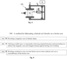
- Fig. 2 is a flow diagram illustrating a method 200 for fabrication of a helical SMD-Coil directly over a magnetic core according to an embodiment the present invention. More specifically the method 200 facilitates the fabrication of the helical conductive winding structure CW of the SMD-Coil 10 shown in Figs. 1A to 1C , directly on a circumference surface of the magnetic core, and may also be used for fabrication of the suitable electrically conductive connection(s)/path(s) CP between the conductive winding structure CW and SMT contacts (SMC1 and/or SMC2) of the surface mounting portion(s) SM. This generally is achieved by utilizing photolithographic processes to form a pattern of the conductive windings on the magnetic core and then electroplating the conductive windings along said pattern. More specifically method 200 includes the following operations as described below.
- a magnetic core FC having a tubular shape as defined above is provided.
- the magnetic core FC provided may include, or be constituted by, sintered magnetic material having magnetic relative permeability ⁇ in the order of at least 100.
- the magnetic core FC is substantially constituted by the magnetic core FC provided (e.g., with no substantial amounts of non-magnetic materials therein).
- a magnetic core of material FC that is temperature stable in the temperature range of 20°C to 60°C is provided (e.g., with temperature coefficient of permeability of less than ⁇ 160ppm/°C).
- a seed layer may be fabricated over a circumference surface/section of the tubular magnetic core FC. This operation may be performed in case where the conductivity of the bare surface of the magnetic core FC is insufficient for electroplating.
- the seed layer may be fabricated by any suitable technique as will be appreciated by those versed in the art, for example by chemically applying a catalyst followed by thin electroless copper coat on the circumference surface/section of the tubular magnetic core FC to increase its electrical conductivity and facilitate the subsequent electroplating. Operation 215 is optional as in cases where the bare surface of the magnetic core is sufficiently conductive for electroplating, there may be no need for fabrication of the seed layer.
- operation 215 may be carried out at different stages of the method 200.
- the catalyst is deposited selectively on the magnetic core FC and not deposited on the photoresist that is applied thereon in operation 220 described below.
- the operation 215 may be carried out only after the operations 220 and 230 described below for fabricating the seed layer at surfaces of the core FC from which the photoresist is removed by photolithography in operation 230.
- the surface of the magnetic core under the photoresist will remain clean of both catalyst and seed layer and the electroless copper will grow substantially only on the exposed surfaces of the magnetic core, at which then the conductive windings will be formed by the electroplating (operation 240 ).
- the optional operation 245 of removing of the remaining photoresists may be obviated as there was no forming of a conductive layer underneath it (note that actual removal of the photoresist may still be required depending on chemical and thermal stability of the photoresist used).
- the operation 215 may be carried out in two stages:
- the removal of the photoresists remaining after the patterning in optional operation 245 may be obviated, since a conductive layer will not be formed of underneath the photoresist. Yet in practice actual removal of the photoresist may still be performed in 245 depending on chemical and thermal stability of the photoresist used. Thus, in some implementations at which removal of the remaining photoresist is not necessitated, a permanent resist (similar to SU8 available as dry-film photoresist) may be used in operation 230 below.
- the deposition of the catalyst and seed layer in operation 215 may be applied to the magnetic core prior to the application of the photoresist in operation 220.
- a conductive layer will exist underneath the photoresist, and operation 245 will be required after the electroplating for stripping out the remaining photoresist and etching the seed layer in between the conductive windings electroplated in operation 240.
- a photoresist layer may be applied to the circumference surface/section of the tubular magnetic core FC from all around (360°).
- the photoresist layer is applied with sufficient thickness (e.g., of at least 8 ⁇ m) in order to facilitate later application of relatively thick electroplating (e.g., at least 6 ⁇ m thick) at regions at which the photoresist layer will be removed by patterning, while without spillage/spread of the electroplated conductive material outside of the pattered regions. This may be advantageous to enable subsequent fabrication of relatively thick conductive windings of the coils having low electric resistance.
- a layer of dry photoresist may be used and may be applied all around (360°) the circumferences of said surface/section of the tubular magnetic core FC.
- the use of dry photoresist may be advantageous in this case as its application to the 3D circumference of said surface/section of the tubular magnetic core FC may be more controllable and uniform (e.g. in thickness) as compared to wet photoresists, and since it facilitates achieving substantially thick photoresist layer suitable for the subsequent fabrication of conductive windings having low resistivity and defined boundaries by electroplating (i.e. this facilitates electroplating of narrow conductive lines of the helical conductive windings with substantial thickness while preventing spread of the electroplating between adjacent lines and thereby facilitate small spacing between them, and thus fabrication of dense windings with small pitch P).
- photolithography is applied to pattern the photoresist layer and form a helical pattern over said circumference surface/section of the tubular magnetic core FC which is covered by the photoresist layer.
- the photolithographic process may include the selective projection of photolithographic light of suitable frequency (e.g., UV light) having on the one hand sufficient power for patterning the photoresists, while on the other hand a power/intensity that is insufficient for causing damage to the underlying magnetic material of the core FC (so as not to damage the core and increase its conductivity).
- the selective projection of the photolithographic light may be carried out by direct scanning of the laser beam on the circumference surface/section of the tubular magnetic core FC and/or by any other suitable technique as will be appreciated by those versed in the art of photolithography after knowing the present invention. It would be appreciated that optionally, in order to apply the photolithographic pattern over the three-dimensional (3D) circumference surface/section of the tubular magnetic core FC, the core may be rotated with respect to the light beam during the projection, while also shifting the magnetic core relative to the light beam (e.g., by moving the relative position of the core or by optical steering the light beam) along the longitudinal axis FX of the core.
- the photoresists used may be a so called “positive” photoresists or a “negative” photoresist, and the projected light pattern is adapted accordingly (as negative or positive pattern) so as to yield the desired helical pattern of exposed regions of the photoresist at which the conductive windings CW will be subsequently electroplated.
- the exposure of the photoresists is then followed by development of the photoresists to expose a helical pattern on the circumference surface/section of the tubular magnetic core FC, from which the photoresist is removed by said development.
- Operation 240 includes electroplating the exposed regions of the magnetic core FC (the helical pattern formed after the development of the photoresist) with conductive material (e.g., copper) to yield said conductive winding CW in the form of a conductive helical coil over the external surface layer of the magnetic core.
- conductive material e.g., copper
- the electroplating is conducted to thickness in the order of about 4 ⁇ m or more.
- remaining photoresists material may be removed from between conductive windings of the helical coil CW.
- the surface conductivity of the magnetic core FC underneath the remaining photoresist material may be above a minimal desired threshold (e.g., due to for example a seed layer if such is fabricated in operation 215 before deposition of the photoresist layer).
- the remaining photoresist may be removed from the core followed by etching of conductive seed layer/material and/or catalyst which may have been located between the photoresist and the magnetic core.
- This operation may be for example carried out in cases where the seed layer under the photoresist that needs to be removed in order to clear shorts across the helix.
- a threshold value whether due to catalyst, seed layer or small intrinsic conductivity of the ferrite, the core resistance (whether due to volumetric or surface conductivity) must be larger about 100 times or more the coil (winding) resistance.
- the resistance of the helical windings from contact to contact is in the order of hundreds of Ohms
- the resistance of the ferrite/magnetic core, flange to flange should be in the order of tens of kilo Ohms.
- the helical SMD-Coil or the conductive windings parts thereof, which are fabricated by method 200 may be coated with a thin layer of varnish or tin coating for protection from oxidation of the conductive windings (e.g., during storage of the coils before assembly of the coils in a sensor/circuit at which time they might be further potted with epoxy for protection).
- a single winding layer may be fabricated by method 200 directly over the magnetic core FC. This may reduce fabrication complexity and costs, while still providing sufficient sensitivity due to the high density (small pitch) of the windings obtained by method 200 and the high core permeability.
- stacked/concentric windings layers may be fabricated by repeating the relevant operations of method 200 while introducing insulation material/layer between the successive conductive layer fabrication, as will be appreciated by those versed in the art.
- method 200 may be adapted for fabrication of the conductive helical coil CW with high density windings, and wherein a pitch of the helical pattern and correspondingly of the windings in said conductive winding structure CW is in the order of, or less than 10 ⁇ m (preferably in some embodiments not exceeding about 8 ⁇ m ) .
- a width of conductive path forming the windings of said conductive helical coil may not exceed 7 ⁇ m (in some embodiments not exceeding 4 ⁇ m ) and a spacing between conductive paths of adjacent windings is in the order of 4 to 5 ⁇ m so as to provide high-density windings over said ferrite core.
- the operations of method 200 may be carried out in order to also fabricate suitable electrically conductive connection(s)/path(s) CP between the conductive winding structure CW and SMT contacts ( SMC1 and/or SMC2 ) of the surface mounting portion(s) SM of the SMD-Coil 10 of the invention.
- the ferrite core FC may be provided furnished with the Surface Mount Portion(s) SM, accordingly optional operation 215 and operation 220 to 240 may be carried out in a similar manner as described above in order also to fabricate the electrically conductive connection(s)/path(s) CP between the conductive winding structure CW and SMT contacts ( SMC1 and/or SMC2 ) of the surface mounting portion(s) SM.
- operation 220 to 240 may be carried out to define the two electric contacts SMC1 and SMC2 on the same mounting portion(s) SM without electrically shorting them.
- the magnetic core FC may be provided with a through conductor CV passing across it generally along its longitude axis FX, and one of the conductive paths CP may be fabricated with the through conductor CV incorporated as part thereof as exemplified in optional markings in Fig. 1C .
- method 200 with the operations described above may be adapted mainly to the fabrication of the coil portion C of the SMD-Coil 10 and the attachment between the coil portion C and surface mounting portion(s) SM and/or the electrical coupling between the conductive winding structure CW of the coil portion C and the SMT contacts (SMC1 and/or SMC2) on the surface mounting portion(s) SM may be performed in a separate process.
- the fabrication system 280 is configured and operable for implementing at least the operation 230 of method 200 described above, so as to apply photolithography over a magnetic/ferrite core FC to which photoresist was applied, to form a helical photoresist pattern suitable for fabrication (e.g., electroplating) of helical conductive windings directly over the magnetic core FC.
- the fabrication system 280 includes a photolithographic light-source LS, such as a UV laser light source with the properties exemplified above, which is suitable for projecting light LL towards the magnetic core FC to apply photolithography to a photoresist layer on the magnetic core FC.
- the fabrication system also includes a handler utility HL which is configured and operable for carrying/holding the ferrite core and applying relative movement between it and the light LL from the photolithographic light-source LS to project (e.g., sequentially), a helical winding pattern on the magnetic core FC.
- a handler utility HL which is configured and operable for carrying/holding the ferrite core and applying relative movement between it and the light LL from the photolithographic light-source LS to project (e.g., sequentially), a helical winding pattern on the magnetic core FC.
- the helical pattern may be projected utilizing a combination of relative rotational movement RM about axis RX and linear movement LM parallel to said axis RX, which may be affected by the handler utility HL (or optical steering of the laser beam) between the magnetic core FC.
- the handler utility HL and a control unit CU of the fabrication system 280 which is adapted for controlling the handler utility HL and the light-source LS, may are configured and operable to apply such relative movement between the magnetic core FC and the photolithographic light-beam LL so as to project a three-dimensional helical pattern of the photolithographic light on the core.
- Fig. 4 a flow diagram of another method 300 for fabrication of the coil portion C of a compact SMD coil 10 according to an embodiment of the invention is provided. More specifically, method 300 is adapted to fabricate a helical coil directly on a magnetic core FC by winding a wire over a circumference the magnetic core.
- a magnetic core FC having a tubular shape is provided.
- the magnetic core FC may include, or be constituted by, sintered, or more preferably fully-sintered magnetic material having magnetic permeability ⁇ in the order of at least 100.
- a magnetic core FC of material that is temperature stable in the temperature range of 20°C to 60°C is provided (e.g., with temperature coefficient of permeability of less than ⁇ 160ppm/°C).
- the magnetic core provided may have a round cross section in the center section which is wound (so as to relieve stress from the wounded wire) while the flange regions may have polygonal/rectangular cross-sections) that the magnetic core is capable of enduring stresses applied thereto by the conductive wire during its winding without substantial damage.
- one or more surface regions of the magnetic core are coated/coupled with a buffer layer/structure of material suitable for relieving mechanical stresses from the magnetic core itself and/or from the wire winded thereon.
- a layer of flexible material such as wax capable of absorbing/mitigating/distributing some of the stresses applied between the core and the thin wire during the winding (thereby preventing both damage to the core as well as breakage of the wire during the winding) or a structurally enforcing material such as polymer, for example coating surfaces of the magnetic core, or provided as "pillars" in corners of the magnetic core (in case its cross-section is polygonal) to absorbed/distribute some of the stresses applied between the core and the thin wire.
- the buffer layer or structure need not be removed after the winding processes (e.g., thereby not potentially forming any gaps between the windings and the core.
- the material may be removable/removed from the core after the wire winding.
- a thin conductive wire (e.g., of characteristic width of about 10 ⁇ m and less than 20 ⁇ ) is provided and winded over the magnetic core to form said conductive winding structure.
- the windings may be performed with one or more layers of winded wires thereby forming a single helical wire structure, or a structure of multiple concentric helixes of wire, over the circumference of the magnetic core.
- the winding of the horizontal helical SMD coils 10H is performed with an odd number of winding layers so that the two ends of the winded wire land on opposite ends of the core to be connected to metallized/contact areas there.
- typically the winding of the vertical helical SMD coils 10V is performed with an even number of layers so that the two ends of the wire land on the bottom face of the core (which is to be installed on the circuit board).
- each end of the wire is attached to a different metallized contact pad on the SMT mount of the bottom face core (with no need to pass the wire through a drill of the ferrite core or externally to the coil).
- winding is performed while mitigating the tension applied on the winded wire so as to prevent tearing of the wire (for example when utilizing conductive wire of 10 ⁇ m in diameter, the maximum tension applied to the wire during the winding does not exceed about 1.4g.
- embodiments of method 300 are adapted to fabrication of a coil portion C of the SMD-Coil 10 of the present invention.
- method 300 as described above is specifically suited for the fabrication of conductive windings utilizing thin conductive wire of characteristic diameter/width in the order of 10 micrometers and less than 20 ⁇ while mitigating pressure/stress applied by the wire on the magnetic core and relieving tension from the wire so as to eliminate or at least reduce and control any damage which maty be affected on the magnetic core by the wire-winding process and also prevent/reduce tearing of the winded conductive wire during the process.
- 10 ⁇ m diameter copper wire e.g., 12-13 ⁇ m including enameled wire insulation
- thinner wire may be winded directly over the core with for example few hundred turns (e.g., 600) in one or more layers.
- the method 300 thereby enables high fabrication throughput of high-density direct winding of thin conductive wire over the magnetic core while with reduced waste/production of damaged-products.
- the method 300 may also implemented for automated/fully automated production of compact coils, Accordingly, a robust method is provided for fabrication of SMD-coils having robust SMT contacts (which are more reliable than soldering wires )
- Methods 200 and 300 described above is generally supplemented by the attachment/furnishing of one or more Surface Mount Portion(s) SM s from one or both ends of the magnetic core FC and electrical connection of their contacts to the coil.
- the Surface Mount Portions SM s may be formed with non-ferromagnetic material (e.g., copper and/or tin) and/or possibly from Nickel, which although being ferromagnetic, may in some cases be used depending on the specific design of the magnetic core and nickel coating used.
- the attachment of the Surface Mount Portions SM s the operation may be conducted prior-to the implementation of method 200 or 300 by which the conductive winding structure CW of the coil portion C is fabricated.
- the attachment of the Surface Mount Portions SM s and/or their electrical connection to the coil may also be conducted during or after the implementation of the method.
- a position sensor 100 which is adapted to measure signals indicative of at least one of a location and orientation of the sensor relative to a magnetic field source.
- the position sensor 100 in each of these embodiments includes a flexible circuit board CB (e.g., foil circuit board or flex PCB or any other suitable flexible circuit surface as will be appreciated by those versed in the art suitable for use with the sensor of the present invention), and at least three helical SMD-coils surface-mounted to the circuit board CB with surface mount technology (SMT).
- a flexible circuit board CB e.g., foil circuit board or flex PCB or any other suitable flexible circuit surface as will be appreciated by those versed in the art suitable for use with the sensor of the present invention
- SMT surface mount technology
- the flexible circuit board CB is folded to an operative configuration at which the at least three helical SMD-coils are arranged such that their magnetic axes FXs are not co-planarly arranged thereby enabling the at least three helical SMD-coils to sense different aspects of a designated external magnetic field, which are indicative of at least one of a location and orientation of the sensor 100 relative to the external magnetic field (i.e., relative to an external magnetic field source). Accordingly, the signals obtained from the at least three SMD coils are utilized to measure/assess at least one of the orientation and location of the sensor 100 relative to one or more magnetic field sources.
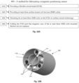
- FIGs. 5A to 5D , 6A to 6D , 7A to 7D and 8A to 8D which exemplify various embodiments of the sensor 100 of the present invention, depict as follows in self-explanatory manner: the figures numbered Figs. #A (i.e. Figs. 5A to 8A ) provide schematic perspective view illustrations showing respective flat/planar circuit layouts of the position sensor 100 according to several embodiments of the present invention in which corresponding arrangements of SMD-Coils 10 are shown surface mounted to a flexible circuit CB (the perspective circuit layout views are shown in Figs. 5A to 8A at a state where the surface of the flexible circuit CB is flat, i.e.
- FIG. 5A to 8A The figures numbered Figs. #B (i.e. Figs. 5B to 8B ) provide schematic side-view illustrations of the position sensor 100 corresponding to the respective embodiments of the sensor shown in Figs. 5A to 8A ; and The figures numbered Figs. #C (i.e. Figs. 5C to 8C ) and Figs. #D (i.e. Figs.
- 5D to 8D are schematic front-view illustrations showing a cross-section of the position sensor circuit as viewed from along a longitudinal axis thereof, after the flexible circuit CB is folded/rolled about respective folding axes FAi and FAo to form the operative configuration of the sensor 100, whereby the figures numbered Figs. #C illustrate embodiments in which the flexible circuit CB is folded such that the coils are located at the outer surface of the folded flexible circuit CB, and the figures numbered Figs. #D illustrate embodiments in which the flexible circuit CB is folded such that the coils are located at the inner surface of the folded flexible circuit CB.
- Figs. 5A to 8D exemplify two optional folding axes FAi and FAo about which the circuit board CB may be folded such that it is formed in a tube-like structure.
- the circuit board CB may be folded about a folding axis is FAo to a tube-like structure (open or closed), with the sensor coils 10 arranged on the outer surface of the tube-like structure of the folded circuit board CB.
- the circuit board CB may be folded/rolled into tube of inner diameter less than 1 mm, preferably even less than 0.9 mm.
- the circuit board CB may be for example foil circuit of thickness of about 10 to 50 microns (e.g., foil of thickness of 0.0127 mm) having printed conductive- tracks/connections CC and solder pads upon which the SMD coils of the sensor can be mounted and soldered).
- the circuit board CB may be folded about a folding axis is FAi to a tube-like structure (open or closed) such that the sensor coils 10 are arranged on the inner surface of the tube-like structure of the folded circuit board CB.
- the folding axis be it FAi or FAo, about which the circuit board CB is folded is also considered and referred to as the longitudinal axis of the sensor 100.
- the at least three helical SMD-coils shown to be disposed with angular intervals of 60° or 120° between them with respect to the designated folding axis is FAo or FAi. It should be however understood that these angular intervals are provided herein only as an example and that in various embodiments of the present invention the at least three coils may be arranged with other angular intervals between them (e.g., possibly with interval of 90°, and/or with different/varying angular intervals between them, while still being operative to sense the position and/or orientation of the sensor relative one or more magnetic field sources.
- the senor 100 may generally be configured with angular intervals of the coils different than those illustrated in the figures in order for example to accommodate various design constraints such as compact/desired arrangement of the coils 10 and/or reducing/adjusting mutual sensing of common magnetic-field signal components by different coils.
- the sensor 100 adapted to measure signals indicative of location and/or orientation thereof relative to a magnetic field source MFo.
- the at least three SMD coils 10 may for example include three horizontal helical SMD coils 10H configured according to the embodiment of the present invention that is described above in relation to Fig. 1B .
- the three SMD coils 10H may be surface mounted to the surface of the circuit board CB via surface mount technology.
- the position sensor 100 of Figs. 5A to 5D is specifically designed to facilitate utilization of the signals obtained from these three SMD coils to determine the orientation of the longitudinal axis FAi or FAo of the sensor 100 relative to the magnetic field source MFo whereby the magnetic field source MIF O is generally located in front of the sensor 100 along a general direction of the longitudinal axis FAi or FAo of the sensor 100.
- the signals obtained from the three SMD coils 10H facilitate to determine the orientation relative to the magnetic field source MFo with respect to two angles (i.e., pitch and yaw) about the longitudinal axis of the sensor 100.
- the three SMD coils 10H may be furnished on the circuit board CB with parallel orientation of their magnetic flux axes FXs relative to the surface of the circuit board CB, and such that their magnetic flux axes FX s are substantially parallel to one another.
- the three SMD coils 10H are arranged on the circuit board CB such that they (specifically their core sections C ) are alighted/justified with respect to straight guideline GL perpendicular to the longitudinal/folding axis FAi or FAo, and such that their magnetic flux axes FXs are substantially parallel to the longitudinal/folding axis FAi or FAo.
- the magnetic flux axes FX s of the three SMD coils 10H are substantially parallel to one another while not being co-planar (so as to facilitate orientation measurements about two angle), and preferably all three SMD coils 10H are (specifically their core sections C ) are aligned with respect to a common reference plane RP (the reference plane may be for example the plane accommodating the guideline GL when the circuit is folded).
- the at least three helical SMD coils 10H which are used in the embodiments of Figs. 5A to 5D to measure the orientation with respect to the magnetic source MFo, are coils of similar configuration (dimensions and inductance/reactance values).
- the position sensor 100 of Figs. 5A to 5D is suitable configured for accurate measurement of the orientation of the sensor relative to magnetic field source MFo positioned generally in front of the three helical SMD coils 10H of the sensor.
- a signal processing circuit (not specifically shown; e.g., a computerized system) which may be connected to the sensor, may operate to determine the measured orientation of the magnetic field source MFo.
- a compact helical SMD coils 10H configured according to the present invention with longitudinal dimension of the core section C extends about 1.2-1.4 mm (and totally about 2mm together with the surface mounting portions), and lateral dimensions (width/diameter) extending in the order of 0.6mm or less and more preferably in the order of 0.5mm, and may yield sensitivity of about ⁇ 0.2 ⁇ V/(Gauss*Hz) thereby enabling accurate measurements of the orientation relative to the magnetic field source MFo.
- sensitivity of about ⁇ 0.2 ⁇ V/(Gauss*Hz)
- the sensor 100 is adapted to measure signals indicative of location and/or orientation thereof relative to a magnetic field source MF L .
- the sensor 100 includes a flexible circuit board CB and three SMD coils whereby: two of the at least three SMD coils 10 are vertical helical SMD coils 10V configured according to the embodiment of Fig. 1C and surface mounted to the surface of the circuit board CB via surface mount technology with vertical / perpendicular orientation of their magnetic flux axes FX relative to the circuit board CB, and one SMD coil of the at least three SMD coils 10 is a horizontal helical SMD coil 10H configured according to Fig.
- the three SMD coils 10 are arranged on the circuit board CB such that when the circuit board CB is flexed/folded/rolled about the folding axis FAi or FAo to its designated operative configuration (as exemplified in Figs. 6B to 6D ), the magnetic flux axes FX s of the three SMD coils 10 are not parallel to one another and span three dimensional coordinates which enable the coils to measure different vectored components in of a magnetic field in their vicinity.
- the two vertical helical SMD coils 10V may be arranged such that when the CB is flexed to its operative state their magnetic flux axes of said two SMD coils are not parallel and are for example in 90° or 120° with respect to one another, and the horizontal helical SMD coil 10H may for example be arranged with its magnetic flux axis relative being parallel to the folding axis FAi or FAo of the circuit board (e.g. optionally in some implementations this may facilitate compact folding of the circuit board).
- the arrangement of the at least three SMD coils 10 with their magnetic flux axes FX spanning three-dimensional coordinates facilitate the measurement of the vector component of magnetic fields in their vicinity thereby enabling to determine the location and/or orientation of the sensor 100 relative to an external source of magnetic field(s) MF L .
- external source of magnetic field(s) MF L generating a plurality of distinguishable magnetic fields (e.g., typically at least three magnetic fields of different frequencies) both the position and orientation of the sensor 100 may be determined.
- both the location and/or orientation of the magnetic field source MF L relative to the sensor 100 may be determined based on the measurement of the magnetic field vector components at the sensor 100
- the two vertical helical SMD coils 10V which are used in the embodiments of Figs. 6A to 6D may be coils of similar configuration (dimensions and inductance/reactance values).
- the vertical helical SMD coils 10V are configured with a core cross-section that is elongated in one lateral dimension (such as a core with elliptical cross-section or rectangular cross-section in which one lateral dimension is larger than the other as exemplified in Fig. 6A ), and vertically furnished on the circuit board CB such of the longer side of their core cross-section is substantially collinear with the folding axis FAi or FAo about which the circuit board CB is to be flexed.
- the position sensor 100 of Figs. 6A to 6D is suitable configured for accurate measurement of the location and/or orientation of the sensor relative to a magnetic field source MF L .
- an SMD-Coil 10V configured with compact configuration according to the present invention and having longitudinal dimension extends about 0.45mm to 0.6mm (typically about 0.5mm or less) along its magnetic axis and with elongated/elliptic cross-section having lateral dimensions of about 0.7mmX2.2mm may yield sensitivity of about 0.1 to 0.2 ⁇ V/(Gauss*Hz)) for sensing magnetic fields in the KHz frequency regime, thereby enabling accurate measurement of the location and orientation of the magnetic field source MF L (note that the measure of sensitivity is indicated here for uniform magnetic fields, and the sensitivity for non-uniform fields may be less).
- the position sensor 100 includes at least five SMD coils 10, which are surface mounted on one or more flexible circuit boards CB (only one circuit board is illustrated in the non-limiting example shown in the figures).
- Three SMD coils of the at least five SMD coils 10 of the sensor 100 may be horizontal helical SMD coils 10H, which may be configured and arranged on the circuit board CB in a similar manner as described above with relation to Figs.
- two SMD coils of the at least five SMD coils 10 of the sensor 100 may be vertical helical SMD coils 10V, which may be configured and arranged on the circuit board CB in a similar manner as the vertical helical SMD coils 10V described above with relation to Figs. 6A to 6D (e.g.
- a second magnetic field source MF L e.g. which may operate to generate magnetic field of a second frequency such as between 1 and 4 KHz.
- the at least five SMD coils 10 may be arranged with various arrangements on the one or more circuit boards CB of the sensor in order to accommodate different prerequisite compact dimensions of the sensor, while packing therein the highly sensitive coils.
- a sensor 100 of specifically narrow tubular shape is provided packing said five SMD-coils 10.
- the three horizontal helical SMD coils 10H are arranged in a first row (e.g.
- the two vertical helical SMD coils 10V may not be arranged in the same row (e.g. may be arranged on the circuit board(s) CB backward from the row of the three horizontal helical SMD coils 10H ) so that a circumference of the circuit board CB needs to accommodate the three horizontal helical SMD coils 10H at one circumference region, and at separate circumference region(s) to accommodate said two vertical helical SMD coils 10V.
- the circuit board CB may be of about 12-15 ⁇ m in thickness and with longitudinal dimension of about L ⁇ 10mm and width of about W ⁇ 2.5-3mm and may be rolled to a tube-like shape of diameter about 1mm or less.
- the three coils 10H which are used to determine the orientation relative to the first magnetic field source MFo, may be similar coils or rectangular circular or elliptic cross-section
- the two additional coils 10V which may be used together with one of said three coils, to determine the orientation/location relative to the second magnetic field source MF L
- coils 10 of the sensors 100 in the above examples are considered to be surface mountable coils (e.g., SMD-coils configured according to the embodiments of the present invention as described in Figs. 1A to 1C ), in other implementations of the sensor 100 contemplated by the inventors, some of the coils may be not SMD-Coils and/or not configured according to the coil configuration described in Figs. 1A to 1C .
- the three coils, which are used to determine the orientation relative to the first magnetic field source MIF O may be SMD-coils configured according to the present invention and the two additional coils which are used to determine the location/orientation relative to the second magnetic field source MF L may optionally be coils of other types, such as air-core coils.
- the senor 100 may be connected to a signal processing circuit (not specifically shown) which may include for example an external analog and/or digital processing circuitry adapted for processing the signals of the SMD-coil(s) 10 to determine the orientation of the sensor relative to the magnetic field source MFo and/or the location/orientation of the sensor relative to the second magnetic field source MF L .
- a signal processing circuit not specifically shown
- an external analog and/or digital processing circuitry adapted for processing the signals of the SMD-coil(s) 10 to determine the orientation of the sensor relative to the magnetic field source MFo and/or the location/orientation of the sensor relative to the second magnetic field source MF L .
- the medical instrument 1000 which may be a compact invasive medical instrument, generally includes a housing H and a magnetic field-based position sensor 100 configured according to the present invention and fixedly furnished at the housing H.
- the medical instrument 1000 is also associated with at least one magnetic-field source MF that is configured and operable for generating a designated magnetic field in its surroundings to enable the magnetic field-based position sensor 100 to determine at least one of its location and orientation relative to the at least one magnetic-field source MF.
- At least one magnetic-field source MF may or may not be enclosed in the housing H and may or may not be integral part of the medical instrument 1000.
- the medical instrument 1000 is associated with several at least one magnetic-field sources MF generating magnetic fields of different properties (e.g., different frequencies) so as to enable measurement of the relative positions of orientations of different parts of the medical instrument 1000.
- the magnetic field-based position sensor 100 is configured according to the invention as described for example in any of the embodiments of Figs.
- SMD-Coils 10 typically a plurality
- a flexible circuit board CB which is arranged within the housing in its operative configuration in which it is flexed/folded/rolled as described above such that the magnetic flux axes of the one or more SMD-Coils 10 are not coplanar. Accordingly in this configuration a highly sensitive and compact position sensor 100 is contained withing small dimensions of the medical instrument.
- a perspective view of a medical instrument 1000 e.g., probe/catheter
- the medical instrument 1000 in this embodiment is exemplifies a configuration of the medical instrument described above with reference to Fig.
- the housing/medical instrument includes a main section M having a longitudinal axis L and a tip section T that is flexibly coupled to at a distal end of the main section M via a banding coupler J, such as a spring or joint, configured such that the orientation of the tip section T can be bent relative to the longitudinal axis L of the housing under applied force F (which may be applied for example when tip section T of the medical instrument is in contact with a body tissue of a patient) to degrees in correspondence with a magnitude and direction of the applied force F.
- the medical instrument 1000 includes the magnetic field source MF O , which may be for example a coil associated with appropriate circuitry for generating a magnetic field.
- the magnetic field source MF O is typically fixedly located at the tip section T and the magnetic field-based position sensor 100, which is typically located within the main section M of the housing (it is noted that in some embodiments an opposite configuration where the magnetic field source MF O may be located at the main section and the position sensor 100 at the tip may be implemented depending on design/dimension constraints of the medical instrument).
- the magnetic field source MFo is configured and operable to generated a magnetic field provides a reference frame indicative of the orientation and possibly also the location of the housing section in which it is furnished (hereinafter and without loss of generality the tip section T ).
- the magnetic field-based position sensor 100 which is located in another body section (hereinafter and without loss of generality the main section M ) which is movable (e.g.
- the rotatable with respect to the section at which the magnetic field source MFo is located (e.g. with respect to the tip section T ) is configured and operable for sensing the magnetic field generated by the magnetic field source MF O and based on said measurements determine/estimate the orientation of the tip section T relative to the main section M, which is generally indicative of the force vector F applied to the tip section (e.g. between the tip and a body tissue when the medical instrument is employed in medical operation).
- the magnetic field source MFo may be for example a coil arranged in the tip section T and generating an alternating magnetic field for example with frequencies in the KHz regime (e.g., 16KHz).
- the coils of the magnetic field source MFo may be arranged such that in a neutral un-bent position of the tip section T relative to the longitudinal axis L of the housing, its magnetic flux axis is substantially colinear/coincides with the longitudinal axis L of the housing.
- the magnetic field-based position sensor 100 is position sensor 100 configured according to the present invention for example the position sensor illustrated in any one of the embodiments of Figs.
- said orientation of the sensor 100 relative to the magnetic field source MFo may be determined based on measurements of the magnetic field generated by the source MFo (which provides a reference frame relative to which the orientation can be determined).
- said force vector F may be determined based on the measured orientation and the properties (e.g., spring constant) of said banding coupler J.
- Fig. 9C a side-view of a medical instrument 1000 according to another embodiment of the present invention is schematically illustrated.
- the medical instrument 1000 in this embodiment incorporates the features of the medical instrument 1000 which reference to Fig. 9B for determining the orientation of the tip section relative to the its main section (e.g., or determine the force applied on the tip) and is also adapted to determine/measure the spatial location and/or orientation of the medical instrument 1000 itself.
- the medical instrument 1000 includes a magnetic field based position sensor 100 of the invention in which at least five coils are included, and is associated with another magnetic field source MF L which is to be located externally to the medical instrument 1000 and configured and operable for generating a second magnetic field, which is distinct from the magnetic field produced by the magnetic field source MIF O (e.g. in frequencies) and which provides a spatial reference frame with respect to which the location and/or the orientation of the medical instrument 1000 may be determined (for example the magnetic field source MF L may be adapted to generate magnetic fields in two or more frequencies distinct from the frequency of the magnetic field source MIF O to thereby enable determination of both the location and the orientation of the medical instrument 1000.
- the magnetic field source MF L may be adapted to generate magnetic fields in two or more frequencies distinct from the frequency of the magnetic field source MIF O to thereby enable determination of both the location and the orientation of the medical instrument 1000.
- the medical instrument 1000 in this embodiment may include a position sensor 100 of the present invention, such as that illustrated in any one of the embodiments of Figs. 7A to 7D and 8A to 8D in which at least five coils/SMD-Coils are included. Accordingly, as described above with reference to these figures, a subset of at least three of these at least five coils may be arranged such that their magnetic flux axes span three-dimensional coordinates thereby enabling to determine a spatial location and/or orientation of medical instrument 1000 by measuring the magnetic field generated by said relative to the magnetic field source MF L (as indicated above both location and orientation may be determined).
- FIG. 10A A method 400 to fabricate a magnetic position sensor 100 suitable for use in a medical instrument is schematically illustrated in a flow diagram in Fig. 10A .
- the method includes the following operations:
- the FCB may be folded/rolled such that the SMD coils mounted thereon face inwardly and/or outwardly relative to the folding axis.
- the SMD coils are arranged on the FCB such that when the FCB is folded/rolled about a certain designated folding axis, the magnetic axes of the SMD coils are not coplanar with respect to one another to thereby facilitate measurement of at least one of a location and orientation of the sensor relative to one or more magnetic field sources.
- the magnetic positioning sensor may be adapted to measure signals indicative of an orientation of the sensor relative to a magnetic field source (e.g. reference MFo in the figures described above).
- the mounting operation 430 may include mounting three of the SMD coils on the FCB such that their magnetic flux axes are parallel to one another and are not co-planar when the FCB is folded to the tubular form to thereby enable measurement of two angles of orientation the relative to the magnetic field source MFo when the latter is located in-front of the three SMD coils with respect to the general direction of their magnetic flux axes.
- the magnetic positioning sensor 10 may be adapted to measure signals indicative of location and orientation of the sensor relative to one or more external magnetic field sources (e.g. reference MF L in the figures described above).
- the mounting operation 430 may include mounting three of the SMD coils such that when the FCB is folded to the tubular form, their magnetic flux axes span 3D coordinates, and thereby enable measurement of the location and orientation of the sensor 100 relative to these one or more external magnetic field sources MF L .
- the magnetic positioning sensor is adapted to measure signals indicative of an orientation of the sensor relative a first magnetic field source MFo and signals indicative of location and orientation of the sensor relative to one or more second external magnetic field sources MF L .
- the at least three SMD coils provided in 420 include at least five SMD coils.
- the mounting in 430 is performed such that: a first subset of at least three of the SMD coils are arranged with their magnetic axes parallel to one another and such that after the FCB folding they remain parallel but not co-planar (to facilitate the orientation measurement relative to the first magnetic field source MFo as indicated above); a second subset of at least three of the SMD coils are arranged such that their magnetic flux axes span 3D coordinates after folding (operation 440 ) of the FCB (to facilitate the location and orientation measurement relative to the second magnetic field source(s) MF L as indicated above).
- Example of such arrangement of the coils is illustrated for instance in Figs. 7A to 8C .
- the mounting may be performed utilizing surface mount technology and may include mounting one or more of the SMD coils 10V with vertical orientation of their magnetic flux axes relative to the FCB surface and/or mounting one or more of the SMD coils 10H with horizontal/parallel orientation of their magnetic flux axes relative to the FCB surface.
- the FCB with the SMD coils mounted thereon is folded/rolled to tubular form with sufficiently narrow outer diameter Do such that it can be fitted within a small/narrow medical instrument.
- the outer diameter Do of the sensor Do after the FCB has been folded/rolled should not exceed about 2 millimeters.
- a tube T may be used to assist proper folding of the FCB.
- the tube T may serve as an inner skeleton about which the FCB is folded as exemplified in Fig. 10B , or otherwise as an outer skeleton within which the folded FCB may be inserted.
- the tube T may be for example a polyimide tube. In the example illustrated in Fig.
- the tube serves as an inner tube about which the FCB is folded and has a characteristic diameter Di of about 0.92mm.
- the FCB is folded thereon to form an outer tube with diameter Do of 1.97mm such that it can be fitted within the narrow medical instrument, and the SMD coils thus reside in the spacing (of about 0.53mm) between the inner and outer diameters as shown in the figure.
- the folding 440 further includes encapsulation (potting) of the electronic components (FCB, SMD coils etc.) of the sensor 100 together with any soldered cable wires connected thereto in order to form the sensor as a robust single piece unit.
- Sensor potting may be performed utilizing for instance UV or thermal adhesive and may be carried out in a single stage process or two-stage process (e.g.
- the empty spaces between the polyimide tube T and the rolled thin FCB with coils and any soldered cable wires connected thereto is filled with adhesive. Potting preferably also anchors any soldered cable wires connected to FCB/coils the cable in order to protect from mechanical stresses which may be applied thereto during insertion to the medical instrument.
- operation 420 of method 400 includes fabricating one or more of the SMD coils utilizing the method of the present invention as described above for instance in relation to Fig. 2 or Fig. 3 .
- the photolithographic coil fabrication technique described in relation to Fig. 2 is used in order to form one or more of the SMD coils with their helical coils directly on the ferrite core.
Landscapes
- Health & Medical Sciences (AREA)
- Life Sciences & Earth Sciences (AREA)
- Physics & Mathematics (AREA)
- Engineering & Computer Science (AREA)
- General Physics & Mathematics (AREA)
- Surgery (AREA)
- Biomedical Technology (AREA)
- Heart & Thoracic Surgery (AREA)
- Animal Behavior & Ethology (AREA)
- General Health & Medical Sciences (AREA)
- Public Health (AREA)
- Veterinary Medicine (AREA)
- Biophysics (AREA)
- Medical Informatics (AREA)
- Molecular Biology (AREA)
- Condensed Matter Physics & Semiconductors (AREA)
- Pathology (AREA)
- Human Computer Interaction (AREA)
- Nuclear Medicine, Radiotherapy & Molecular Imaging (AREA)
- Anesthesiology (AREA)
- Manufacturing & Machinery (AREA)
- Pulmonology (AREA)
- Hematology (AREA)
- Robotics (AREA)
- Microelectronics & Electronic Packaging (AREA)
- Measurement Of Length, Angles, Or The Like Using Electric Or Magnetic Means (AREA)
- Measurement And Recording Of Electrical Phenomena And Electrical Characteristics Of The Living Body (AREA)
- Coils Or Transformers For Communication (AREA)
- Media Introduction/Drainage Providing Device (AREA)
Applications Claiming Priority (2)
| Application Number | Priority Date | Filing Date | Title |
|---|---|---|---|
| US202363523440P | 2023-06-27 | 2023-06-27 | |
| US18/749,244 US20250009247A1 (en) | 2023-06-27 | 2024-06-20 | System and method of sensing catheters location and force |
Publications (1)
| Publication Number | Publication Date |
|---|---|
| EP4483799A1 true EP4483799A1 (fr) | 2025-01-01 |
Family
ID=91699904
Family Applications (1)
| Application Number | Title | Priority Date | Filing Date |
|---|---|---|---|
| EP24184690.6A Pending EP4483799A1 (fr) | 2023-06-27 | 2024-06-26 | Système et procédé de détection de la position et de la force d'un cathéter |
Country Status (5)
| Country | Link |
|---|---|
| US (1) | US20250009247A1 (fr) |
| EP (1) | EP4483799A1 (fr) |
| JP (1) | JP2025005433A (fr) |
| CN (1) | CN119197275A (fr) |
| IL (1) | IL313896A (fr) |
Families Citing this family (1)
| Publication number | Priority date | Publication date | Assignee | Title |
|---|---|---|---|---|
| US20250255509A1 (en) * | 2024-02-14 | 2025-08-14 | St. Jude Medical International Holding S.á r.l | Magnetic position sensor |
Citations (3)
| Publication number | Priority date | Publication date | Assignee | Title |
|---|---|---|---|---|
| US1569320A (en) | 1925-02-20 | 1926-01-12 | Maurice F Griffin | Trunk |
| EP2196143A1 (fr) * | 2008-12-03 | 2010-06-16 | Biosense Webster, Inc. | Sonde de détection de pression haute sensibilité |
| EP1806756B1 (fr) * | 2006-01-06 | 2017-08-30 | Biosense Webster, Inc. | Bobines miniatures sur noyau comprenant un circuit imprimé |
-
2024
- 2024-06-20 US US18/749,244 patent/US20250009247A1/en active Pending
- 2024-06-25 IL IL313896A patent/IL313896A/en unknown
- 2024-06-26 CN CN202410836772.2A patent/CN119197275A/zh active Pending
- 2024-06-26 JP JP2024102728A patent/JP2025005433A/ja active Pending
- 2024-06-26 EP EP24184690.6A patent/EP4483799A1/fr active Pending
Patent Citations (4)
| Publication number | Priority date | Publication date | Assignee | Title |
|---|---|---|---|---|
| US1569320A (en) | 1925-02-20 | 1926-01-12 | Maurice F Griffin | Trunk |
| EP1806756B1 (fr) * | 2006-01-06 | 2017-08-30 | Biosense Webster, Inc. | Bobines miniatures sur noyau comprenant un circuit imprimé |
| US8535308B2 (en) | 2007-10-08 | 2013-09-17 | Biosense Webster (Israel), Ltd. | High-sensitivity pressure-sensing probe |
| EP2196143A1 (fr) * | 2008-12-03 | 2010-06-16 | Biosense Webster, Inc. | Sonde de détection de pression haute sensibilité |
Non-Patent Citations (1)
| Title |
|---|
| UCHIYAMA S ET AL: "Novel MEMS-based fabrication technology of micro solenoid-type inductor", JOURNAL OF MICROMECHANICS AND MICROENGINEERING, INSTITUTE OF PHYSICS PUBLISHING, BRISTOL, GB, vol. 23, no. 11, 24 October 2013 (2013-10-24), pages 114009, XP020252634, ISSN: 0960-1317, [retrieved on 20131024], DOI: 10.1088/0960-1317/23/11/114009 * |
Also Published As
| Publication number | Publication date |
|---|---|
| JP2025005433A (ja) | 2025-01-16 |
| US20250009247A1 (en) | 2025-01-09 |
| CN119197275A (zh) | 2024-12-27 |
| IL313896A (en) | 2025-01-01 |
Similar Documents
| Publication | Publication Date | Title |
|---|---|---|
| US7924000B2 (en) | Miniature coils on core with printed circuit | |
| US8710824B2 (en) | Voltage detector having voltage detection printed board | |
| US8629674B2 (en) | Current detection printed board, voltage detection printed board, current/voltage detection printed board, current/voltage detector, current detector and voltage detector | |
| JP5427459B2 (ja) | 高ダイナミックレンジを有する直交高周波電圧/電流センサ | |
| EP1264188A1 (fr) | Enroulement de rogowski de grande precision | |
| EP4483799A1 (fr) | Système et procédé de détection de la position et de la force d'un cathéter | |
| US6344781B1 (en) | Broadband microwave choke and a non-conductive carrier therefor | |
| US8146239B2 (en) | Method of forming microcoil with conducting trace and attaching trace | |
| JP2008504054A (ja) | Rf場で使用する送信線 | |
| JPWO2005029099A1 (ja) | 電流測定装置及び試験装置と、これに用いる同軸ケーブル及び集合ケーブル | |
| JP2002156430A (ja) | 磁界プローブ | |
| EP4510154B1 (fr) | Système et procédé de détection de la position et de la force d'un cathéter | |
| JP2004111831A (ja) | 空芯コイル | |
| JP2005085968A (ja) | 巻線型インダクタ及びその製造方法 | |
| CN119375529A (zh) | 将分流电阻器与罗果夫斯基线圈相结合的电流监视器 | |
| JPH11168341A (ja) | 信号遅延装置 |
Legal Events
| Date | Code | Title | Description |
|---|---|---|---|
| PUAI | Public reference made under article 153(3) epc to a published international application that has entered the european phase |
Free format text: ORIGINAL CODE: 0009012 |
|
| STAA | Information on the status of an ep patent application or granted ep patent |
Free format text: STATUS: THE APPLICATION HAS BEEN PUBLISHED |
|
| AK | Designated contracting states |
Kind code of ref document: A1 Designated state(s): AL AT BE BG CH CY CZ DE DK EE ES FI FR GB GR HR HU IE IS IT LI LT LU LV MC ME MK MT NL NO PL PT RO RS SE SI SK SM TR |
|
| STAA | Information on the status of an ep patent application or granted ep patent |
Free format text: STATUS: REQUEST FOR EXAMINATION WAS MADE |
|
| 17P | Request for examination filed |
Effective date: 20250304 |
|
| STAA | Information on the status of an ep patent application or granted ep patent |
Free format text: STATUS: EXAMINATION IS IN PROGRESS |
|
| 17Q | First examination report despatched |
Effective date: 20250530 |