EP4485525A1 - Qfn-verkapselte halbleiteranordnung und verfahren zu deren herstellung - Google Patents
Qfn-verkapselte halbleiteranordnung und verfahren zu deren herstellung Download PDFInfo
- Publication number
- EP4485525A1 EP4485525A1 EP24182612.2A EP24182612A EP4485525A1 EP 4485525 A1 EP4485525 A1 EP 4485525A1 EP 24182612 A EP24182612 A EP 24182612A EP 4485525 A1 EP4485525 A1 EP 4485525A1
- Authority
- EP
- European Patent Office
- Prior art keywords
- semiconductor device
- packaged semiconductor
- qfn
- die
- thickness
- Prior art date
- Legal status (The legal status is an assumption and is not a legal conclusion. Google has not performed a legal analysis and makes no representation as to the accuracy of the status listed.)
- Withdrawn
Links
Images


Classifications
-
- H—ELECTRICITY
- H10—SEMICONDUCTOR DEVICES; ELECTRIC SOLID-STATE DEVICES NOT OTHERWISE PROVIDED FOR
- H10W—GENERIC PACKAGES, INTERCONNECTIONS, CONNECTORS OR OTHER CONSTRUCTIONAL DETAILS OF DEVICES COVERED BY CLASS H10
- H10W70/00—Package substrates; Interposers; Redistribution layers [RDL]
- H10W70/40—Leadframes
- H10W70/411—Chip-supporting parts, e.g. die pads
- H10W70/415—Leadframe inner leads serving as die pads
-
- H—ELECTRICITY
- H10—SEMICONDUCTOR DEVICES; ELECTRIC SOLID-STATE DEVICES NOT OTHERWISE PROVIDED FOR
- H10W—GENERIC PACKAGES, INTERCONNECTIONS, CONNECTORS OR OTHER CONSTRUCTIONAL DETAILS OF DEVICES COVERED BY CLASS H10
- H10W74/00—Encapsulations, e.g. protective coatings
- H10W74/10—Encapsulations, e.g. protective coatings characterised by their shape or disposition
- H10W74/111—Encapsulations, e.g. protective coatings characterised by their shape or disposition the semiconductor body being completely enclosed
-
- H—ELECTRICITY
- H10—SEMICONDUCTOR DEVICES; ELECTRIC SOLID-STATE DEVICES NOT OTHERWISE PROVIDED FOR
- H10W—GENERIC PACKAGES, INTERCONNECTIONS, CONNECTORS OR OTHER CONSTRUCTIONAL DETAILS OF DEVICES COVERED BY CLASS H10
- H10W74/00—Encapsulations, e.g. protective coatings
- H10W74/01—Manufacture or treatment
-
- H—ELECTRICITY
- H10—SEMICONDUCTOR DEVICES; ELECTRIC SOLID-STATE DEVICES NOT OTHERWISE PROVIDED FOR
- H10W—GENERIC PACKAGES, INTERCONNECTIONS, CONNECTORS OR OTHER CONSTRUCTIONAL DETAILS OF DEVICES COVERED BY CLASS H10
- H10W74/00—Encapsulations, e.g. protective coatings
- H10W74/01—Manufacture or treatment
- H10W74/014—Manufacture or treatment using batch processing
-
- H—ELECTRICITY
- H10—SEMICONDUCTOR DEVICES; ELECTRIC SOLID-STATE DEVICES NOT OTHERWISE PROVIDED FOR
- H10W—GENERIC PACKAGES, INTERCONNECTIONS, CONNECTORS OR OTHER CONSTRUCTIONAL DETAILS OF DEVICES COVERED BY CLASS H10
- H10W74/00—Encapsulations, e.g. protective coatings
- H10W74/10—Encapsulations, e.g. protective coatings characterised by their shape or disposition
-
- H—ELECTRICITY
- H10—SEMICONDUCTOR DEVICES; ELECTRIC SOLID-STATE DEVICES NOT OTHERWISE PROVIDED FOR
- H10W—GENERIC PACKAGES, INTERCONNECTIONS, CONNECTORS OR OTHER CONSTRUCTIONAL DETAILS OF DEVICES COVERED BY CLASS H10
- H10W90/00—Package configurations
-
- H—ELECTRICITY
- H10—SEMICONDUCTOR DEVICES; ELECTRIC SOLID-STATE DEVICES NOT OTHERWISE PROVIDED FOR
- H10W—GENERIC PACKAGES, INTERCONNECTIONS, CONNECTORS OR OTHER CONSTRUCTIONAL DETAILS OF DEVICES COVERED BY CLASS H10
- H10W90/00—Package configurations
- H10W90/811—Multiple chips on leadframes
-
- H—ELECTRICITY
- H10—SEMICONDUCTOR DEVICES; ELECTRIC SOLID-STATE DEVICES NOT OTHERWISE PROVIDED FOR
- H10W—GENERIC PACKAGES, INTERCONNECTIONS, CONNECTORS OR OTHER CONSTRUCTIONAL DETAILS OF DEVICES COVERED BY CLASS H10
- H10W95/00—Packaging processes not covered by the other groups of this subclass
-
- H—ELECTRICITY
- H10—SEMICONDUCTOR DEVICES; ELECTRIC SOLID-STATE DEVICES NOT OTHERWISE PROVIDED FOR
- H10W—GENERIC PACKAGES, INTERCONNECTIONS, CONNECTORS OR OTHER CONSTRUCTIONAL DETAILS OF DEVICES COVERED BY CLASS H10
- H10W70/00—Package substrates; Interposers; Redistribution layers [RDL]
- H10W70/40—Leadframes
- H10W70/421—Shapes or dispositions
-
- H—ELECTRICITY
- H10—SEMICONDUCTOR DEVICES; ELECTRIC SOLID-STATE DEVICES NOT OTHERWISE PROVIDED FOR
- H10W—GENERIC PACKAGES, INTERCONNECTIONS, CONNECTORS OR OTHER CONSTRUCTIONAL DETAILS OF DEVICES COVERED BY CLASS H10
- H10W70/00—Package substrates; Interposers; Redistribution layers [RDL]
- H10W70/40—Leadframes
- H10W70/421—Shapes or dispositions
- H10W70/424—Cross-sectional shapes
-
- H—ELECTRICITY
- H10—SEMICONDUCTOR DEVICES; ELECTRIC SOLID-STATE DEVICES NOT OTHERWISE PROVIDED FOR
- H10W—GENERIC PACKAGES, INTERCONNECTIONS, CONNECTORS OR OTHER CONSTRUCTIONAL DETAILS OF DEVICES COVERED BY CLASS H10
- H10W72/00—Interconnections or connectors in packages
- H10W72/01—Manufacture or treatment
- H10W72/0198—Manufacture or treatment batch processes
-
- H—ELECTRICITY
- H10—SEMICONDUCTOR DEVICES; ELECTRIC SOLID-STATE DEVICES NOT OTHERWISE PROVIDED FOR
- H10W—GENERIC PACKAGES, INTERCONNECTIONS, CONNECTORS OR OTHER CONSTRUCTIONAL DETAILS OF DEVICES COVERED BY CLASS H10
- H10W72/00—Interconnections or connectors in packages
- H10W72/071—Connecting or disconnecting
- H10W72/073—Connecting or disconnecting of die-attach connectors
-
- H—ELECTRICITY
- H10—SEMICONDUCTOR DEVICES; ELECTRIC SOLID-STATE DEVICES NOT OTHERWISE PROVIDED FOR
- H10W—GENERIC PACKAGES, INTERCONNECTIONS, CONNECTORS OR OTHER CONSTRUCTIONAL DETAILS OF DEVICES COVERED BY CLASS H10
- H10W72/00—Interconnections or connectors in packages
- H10W72/071—Connecting or disconnecting
- H10W72/075—Connecting or disconnecting of bond wires
-
- H—ELECTRICITY
- H10—SEMICONDUCTOR DEVICES; ELECTRIC SOLID-STATE DEVICES NOT OTHERWISE PROVIDED FOR
- H10W—GENERIC PACKAGES, INTERCONNECTIONS, CONNECTORS OR OTHER CONSTRUCTIONAL DETAILS OF DEVICES COVERED BY CLASS H10
- H10W72/00—Interconnections or connectors in packages
- H10W72/851—Dispositions of multiple connectors or interconnections
- H10W72/874—On different surfaces
- H10W72/884—Die-attach connectors and bond wires
-
- H—ELECTRICITY
- H10—SEMICONDUCTOR DEVICES; ELECTRIC SOLID-STATE DEVICES NOT OTHERWISE PROVIDED FOR
- H10W—GENERIC PACKAGES, INTERCONNECTIONS, CONNECTORS OR OTHER CONSTRUCTIONAL DETAILS OF DEVICES COVERED BY CLASS H10
- H10W74/00—Encapsulations, e.g. protective coatings
-
- H—ELECTRICITY
- H10—SEMICONDUCTOR DEVICES; ELECTRIC SOLID-STATE DEVICES NOT OTHERWISE PROVIDED FOR
- H10W—GENERIC PACKAGES, INTERCONNECTIONS, CONNECTORS OR OTHER CONSTRUCTIONAL DETAILS OF DEVICES COVERED BY CLASS H10
- H10W74/00—Encapsulations, e.g. protective coatings
- H10W74/01—Manufacture or treatment
- H10W74/016—Manufacture or treatment using moulds
-
- H—ELECTRICITY
- H10—SEMICONDUCTOR DEVICES; ELECTRIC SOLID-STATE DEVICES NOT OTHERWISE PROVIDED FOR
- H10W—GENERIC PACKAGES, INTERCONNECTIONS, CONNECTORS OR OTHER CONSTRUCTIONAL DETAILS OF DEVICES COVERED BY CLASS H10
- H10W90/00—Package configurations
- H10W90/701—Package configurations characterised by the relative positions of pads or connectors relative to package parts
- H10W90/731—Package configurations characterised by the relative positions of pads or connectors relative to package parts of die-attach connectors
- H10W90/736—Package configurations characterised by the relative positions of pads or connectors relative to package parts of die-attach connectors between a chip and a stacked lead frame, conducting package substrate or heat sink
-
- H—ELECTRICITY
- H10—SEMICONDUCTOR DEVICES; ELECTRIC SOLID-STATE DEVICES NOT OTHERWISE PROVIDED FOR
- H10W—GENERIC PACKAGES, INTERCONNECTIONS, CONNECTORS OR OTHER CONSTRUCTIONAL DETAILS OF DEVICES COVERED BY CLASS H10
- H10W90/00—Package configurations
- H10W90/701—Package configurations characterised by the relative positions of pads or connectors relative to package parts
- H10W90/751—Package configurations characterised by the relative positions of pads or connectors relative to package parts of bond wires
- H10W90/752—Package configurations characterised by the relative positions of pads or connectors relative to package parts of bond wires between stacked chips
-
- H—ELECTRICITY
- H10—SEMICONDUCTOR DEVICES; ELECTRIC SOLID-STATE DEVICES NOT OTHERWISE PROVIDED FOR
- H10W—GENERIC PACKAGES, INTERCONNECTIONS, CONNECTORS OR OTHER CONSTRUCTIONAL DETAILS OF DEVICES COVERED BY CLASS H10
- H10W90/00—Package configurations
- H10W90/701—Package configurations characterised by the relative positions of pads or connectors relative to package parts
- H10W90/751—Package configurations characterised by the relative positions of pads or connectors relative to package parts of bond wires
- H10W90/754—Package configurations characterised by the relative positions of pads or connectors relative to package parts of bond wires between a chip and a stacked insulating package substrate, interposer or RDL
-
- H—ELECTRICITY
- H10—SEMICONDUCTOR DEVICES; ELECTRIC SOLID-STATE DEVICES NOT OTHERWISE PROVIDED FOR
- H10W—GENERIC PACKAGES, INTERCONNECTIONS, CONNECTORS OR OTHER CONSTRUCTIONAL DETAILS OF DEVICES COVERED BY CLASS H10
- H10W90/00—Package configurations
- H10W90/701—Package configurations characterised by the relative positions of pads or connectors relative to package parts
- H10W90/751—Package configurations characterised by the relative positions of pads or connectors relative to package parts of bond wires
- H10W90/756—Package configurations characterised by the relative positions of pads or connectors relative to package parts of bond wires between a chip and a stacked lead frame, conducting package substrate or heat sink
-
- H—ELECTRICITY
- H10—SEMICONDUCTOR DEVICES; ELECTRIC SOLID-STATE DEVICES NOT OTHERWISE PROVIDED FOR
- H10W—GENERIC PACKAGES, INTERCONNECTIONS, CONNECTORS OR OTHER CONSTRUCTIONAL DETAILS OF DEVICES COVERED BY CLASS H10
- H10W90/00—Package configurations
- H10W90/701—Package configurations characterised by the relative positions of pads or connectors relative to package parts
- H10W90/791—Package configurations characterised by the relative positions of pads or connectors relative to package parts of direct-bonded pads
- H10W90/792—Package configurations characterised by the relative positions of pads or connectors relative to package parts of direct-bonded pads between multiple chips
-
- H—ELECTRICITY
- H10—SEMICONDUCTOR DEVICES; ELECTRIC SOLID-STATE DEVICES NOT OTHERWISE PROVIDED FOR
- H10W—GENERIC PACKAGES, INTERCONNECTIONS, CONNECTORS OR OTHER CONSTRUCTIONAL DETAILS OF DEVICES COVERED BY CLASS H10
- H10W90/00—Package configurations
- H10W90/701—Package configurations characterised by the relative positions of pads or connectors relative to package parts
- H10W90/791—Package configurations characterised by the relative positions of pads or connectors relative to package parts of direct-bonded pads
- H10W90/794—Package configurations characterised by the relative positions of pads or connectors relative to package parts of direct-bonded pads between a chip and a stacked insulating package substrate, interposer or RDL
Definitions
- This disclosure relates to integrated circuit (IC) packaging. More particularly, this disclosure relates to a quad-flat-no-leads (QFN) packaged semiconductor devices and a method of making thereof.
- IC integrated circuit
- QFN quad-flat-no-leads
- Limitations on the board level reliability and solder joint reliability of QFN packaging are mainly caused by the mismatch of CTE (coefficient of thermal expansion) between the EMC compound and the metal lead frame.
- CTE coefficient of thermal expansion
- solder breaks are easy to occur at bond wires around the QFN. This is mainly because a lot of stress is concentrated at the top of the bond wires around the QFN, and solder is more likely to detach or break at the bond wires around the QFN than in the middle area of the QFN.
- reducing the thermal expansion mismatch effects between the package EMC compound and the metal lead frame may improve the board level reliability and solder joint reliability of QFN package.
- a QFN packaged semiconductor device having a bottom surface
- the QFN packaged semiconductor device comprising: a die pad on the bottom surface; a die on the die pad; a plurality of leads spaced apart from the die pad and around a peripheral region of the bottom surface; a plurality of bond wires connecting the die and the leads; a molding compound covering the die and the bond wires, wherein the QFN packaged semiconductor device has a first thickness in a central region and a second thickness across the peripheral region, and wherein the second thickness is less than the first thickness.
- the peripheral region surrounds the central region.
- a thickness of the molding compound in the central region is in a range between 0.7 and 3 times a thickness of the molding compound in the peripheral region.
- the central region extends beyond a perimeter of the die by a distance which is in a range between 0.7 and 1.3 times a thickness of the molding compound in the central region.
- the peripheral region extends inwards from the perimeter of the device by a distance which is in a range between 1 and 1.3 times an exposed length of the leads on the bottom surface.
- a thickness of the peripheral region is 0.2 and 0.4mm.
- the central region has a first top surface, and a distance from the first top surface to a top surface of the die is in a range between 0.4 and 0.7 mm.
- the central region has a first top surface and first side faces
- the peripheral region has a second top surface and second side faces and the angle between the second top surface and the first side face is a right angle.
- the angle between the second top surface and the first side face is an obtuse angle.
- each first side face is a flat surface. In one or more other embodiments, each first side face is a curved surface.
- a method of manufacturing a QFN packaged semiconductor device having a bottom surface, and comprising a die pad on the bottom surface, and a plurality of leads spaced apart from the die pad and around a peripheral region of the bottom surface, the method comprising: attaching a die on a die pad; forming wirebonds between the die and a plurality of leads; encapsulating the die and wirebonds with a molding compound, such that the QFN packaged semiconductor device has a first thickness in a central region and a second thickness across the peripheral region of the QFN packaged semiconductor device, wherein the second thickness is less than the first thickness; and singulating the QFN package.
- the peripheral region surrounds the central region.
- a thickness of the molding compound in the central region is in a range between 0.7 and 3 times a thickness of the molding compound in the peripheral region.
- the peripheral region extends inwards from the perimeter of the device by a distance which is between 1 and 1.3 times an exposed length of the leads on the bottom surface.
- the method further comprises: forming a second thickness in the peripheral region by sawing the molding compound of the peripheral region.
- a thickness of the peripheral region is in a range between 0.2 and 0.6mm.
- each central region has a first top surface and first side faces
- each peripheral region has a second top surface and second side faces
- the angle between the second top surface and the first side face is a right angle.
- the angle between the second top surface and the first side face is an obtuse angle.
- the first side face is a flat surface. In one or more other embodiments, the first side face is a curved surface.
- the thickness of the peripheral region of the molding compound around the QFN package is reduced.
- the stress above the leads which results from the mismatch of thermal expansion coefficient between, on the one part, the package molding compound and on hte other part the die and/or the metal lead frame, is reduced.
- the method further comprises: forming a second thickness in the peripheral region by sawing the molding compound of the peripheral region.
- the method further comprises: forming a second thickness in a peripheral region by adding a convex part in a mold of the molding compound.
- a thickness of the peripheral region is in a range between 0.2 and 0.6mm.
- the central region has a first top surface and first side faces
- the peripheral region has a second top surface and second side faces
- the angle between the second top surface and the first side face is a right angle or an obtuse angle
- central region has first side faces, and the first side face is a flat surface or a curved surface.
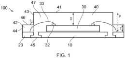
- the QFN packaged semiconductor device 100 comprises: a die pad 10, a plurality of leads 20, a die 30, which is typically rectangular or square and may also be referred to as a semiconductor die, and molding compound 40.
- the leads 20 typically comprise copper or a copper alloy.
- the die 30 is mounted on the die pad 10, which may also be referred to as a die paddle, typically by means of a conductive epoxy or other means known to the skilled person.
- the die pad 10 is typically rectangular and may be square and is generally larger than the die 30.
- the die pad 10 is generally centrally located, and a lower face of the die pad forms part of the bottom surface of the QFN packaged semiconductor device 100, that is to say it is away from the periphery of the QFN packaged semiconductor device 100.
- the leads 20 surround the die 30, typically on all four sides of the die 30 and die pad 10, and are spaced apart therefrom, with molding compound 40 therebetween.
- the leads 30 and the die pad 10 are formed from a same lead frame, and are initially integral but are then separated during the assembly process.
- Bond wires 33 are shown connecting bond pads 32 on the top surface of die 30 to the leads 20.
- the structure is encapsulated in the molding compound 40 except on an underside, or lower-most surface of the die pad 10 and leads 20. As shown in the figure, the lower-most surface and the outermost ends of the leads 20 are exposed and are not encapsulated or covered by molding compound 40.
- the molding compound 40 has a central region 47 and a peripheral region 42.
- the central region 47 is a central region of the molding compound 40.
- the peripheral region 42 is a peripheral region of the molding compound 40.
- the central region 47 is generally centrally located above the die 30, that is to say it is away from the periphery of the QFN packaged semiconductor device 100.
- the peripheral region 42 is above the leads 20 around the periphery of the QFN packaged semiconductor device 100.
- the central region 47 has a thickness corresponding to the full thickness of the molding compound. This part may be described as having a full thickness and may be termed a full thickness part.
- the peripheral region 42 may be thinned during the assembly process, and thus may be described as a half-thickness area.
- Each central region 47 has a first top surface 41 and first side faces 43
- each peripheral region 42 has a second top surface 46 and second side faces 44, wherein each first side face 43 extends between the first top surface 41 and the second top 46 surface and is at an angle ⁇ to the second top surface 46, and each second side face 44 extends vertically between the second top surface 46 and the bottom surface 45.
- the first side face 43 may be a flat surface.
- the angle ⁇ may be a right angle.
- a thickness T of the peripheral region 42 may typically be within a range 0.1-0.4mm.
- the distance D from the top surface 41 of the molding compound 40 to the top surface of the die 30 may typically be within a range 0.4-0.7mm.
- the thickness T may be one fifth to four fifths of the distance D.
- the thickness T is less than the thickness of molding compound above the leads of a conventional QFN package, shown as "P" in FIG. 1 .
- the molding compound is not substantially thicker, around the peripheral region, and in particular above the leads, than it is in the central region. This may reduce or even completely avoid the problems associated with a difference in coefficient of thermal expansion (CTE) between the moulding compound and other parts of the packaged semiconductor device, in particular the semiconductor die 30 and the die pad 10 and leads 20.
- CTE coefficient of thermal expansion
- the CTE difference can result in an increased stress and/or strain occurring around the peripheral region, leading to potential delamination or failure of solder joints.
- the moulding compound according to embodiments of the present disclosure more closely resembles a conformal coating or conformal covering of the die mounted on the lead frame (separated into electrically isolated die pad 10 and leads 20).
- Providing the moulding compound as a conformal coating or resembling or close to a conformal coating may, again, more equally distribute the stress and/or strain resulting from differences in CTE between the moulding compound 40 and either the die 30 or the die pad 10 and leads 20, thereby, again, reducing the likelihood of delamination or solder joint failure.
- the QFN packaged semiconductor device 200 comprises: a die pad 10, a plurality of leads 20, a die 30.
- Each central region 47 has a first top surface 41 and first side faces 43
- each peripheral region 42 has a second top surface 46 and second side faces 44, wherein each first side face 43 extends between the first top surface 41 and the second top 46 surface and is at an angle ⁇ to the second top surface 46, and each second side face 44 extends vertically between the second top surface 46 and the QFN bottom surface 45.
- the first side faces 43 may be flat surfaces.
- the angle ⁇ may be an obtuse angle. That is to say the top of central region 47 is smaller than the bottom.
- Providing sloping sidewalls may help to facilitate demoulding.
- removal, by vertical ejection of the packaged semiconductor device 200 from an injection molding tool which may be used to encapsulate the mounted semiconductor die with the molding compound is generally much easier in the case that there are no vertical surfaces of the molded device. This is because a vertical surface may "stick" against the vertical tool-wall during ejections.
- the thickness T of the peripheral region 42 may conveniently be 0.1-0.4mm.
- the distance D from the top surface 41 of the molding compound 40 to the top surface of the die 30 may conveniently be 0.4-0.7mm.
- the thickness T may typically be one fifth to four fifths of the distance D.
- the leads 20 are thinner than, and less rigid than, the combination of the die pad 10 and the mounted die 30, an equal bending force or stress applied to the leads, due to CTE differences may provide more deflection or strain of the leads 20 than of the die 30 mounted on the die pad 10. It may thus be desirable that the thickness T of the moulding compound above the leads 20 is less than the distance D which corresponds to the thickness of the molding compound above the die 30, in order to reduce the stress at the leads 20 relative to the stress at the die 1030.
- the QFN packaged semiconductor device 300 comprises: a die pad 10, a plurality of leads 20, a die 30.
- Each central region 47 has a first top surface 41 and first side faces 43
- each peripheral region 42 has a second top surface 46 and second side faces 44, wherein each first side face 43 extending between the first top surface 41 and the second top 46 surface, and each second side face 44 extending vertically between the second top surface 46 and the QFN bottom surface 45.
- the first side faces 43 may be curved surfaces.
- the approximate thickness of the peripheral region 42 is T, which may conveniently be 0.1-0.4mm.
- the distance from the first top surface 41 of the molding compound 40 to the top surface of the die 30 is D, and D may conveniently be 0.4-0.7mm.
- the thickness T may typically be one fifth to four fifths of the distance D.
- Providing a curved profile to the thinner region of the moulding compound, and in particular a convex shape such as that shown in figure 3 may be convenient to facilitate moulding in a shaped mould tool, as discussed above.
- the profile is provided by the shape of a mould tool, corners 48 between the shaped sidewalls or first side faces 43 and the top surface, and the corner 49 between the shaped sidewalls and the second faces 43, may conveniently be rounded (not shown) in order to simplify the injection moulding process, as will be familiar to the skilled person.
- the shaped profile may be provided by a partial cut through the package device by a saw blade; in this case, the corners need not be rounded, but may be sharp, as shown in figure 3 .
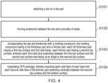
- FIG. 4 shows a flow chart illustrating a method of manufacturing a QFN packaged semiconductor device according to one or more embodiments of the present invention.
- the QFN packaged semiconductor has a bottom surface and comprises a die pad on the bottom surface, and a plurality of leads spaced apart from the die pad and around a peripheral region of the bottom surface.
- the method comprises: S101, attaching a die on a die pad; S102 ("forming wirebonds between the die and a plurality of leads"), forming wirebonds between the die and a plurality of leads; S103, ("encapsulating the die and wirebonds with a molding compound, the molding compound having a full thickness part and a thinner part, each full thickness part having a first top surface and first side faces, each thinner part having a second top surface, wherein each first side face extending between the first top surface and the second top surface and being at an angle to the second top surface”) encapsulating the die and wirebonds with a molding compound having a central region and a peripheral region, wherein the height of the peripheral region is lower than that of the central region; and S104 (“singulating QFN package, thereby exposing each side face of each lead and each second side face of the thinner part extending vertically between the second top surface and the bottom surface”), singulating the QFN package.
- each central region has a first top surface and first side faces, each peripheral region having a second top surface, wherein each first side face extending between the first top surface and the second top surface and being at an angle to the second top surface.
- the first method is to form the peripheral region of the molding compound that is above the leads initially at full thickness, and subsequently remove a top part or portion, for instance by making a partial cut with a saw or a cutting wheel;
- a second method is to use a shaped mold tool used during injection molding of the molding compound. This may be achieved, for example, by adding a convex part, to form a frame around the periphery of the upper half of the molding tool. Since the molding compound fills the space between the mold and the assembly of the die on the die-pad and the leads, adding a convex part to the mold, reduces the amount of molding compound which can be injection.
- the convex part corresponds to the inverse of the position and shape of the desired peripheral region and forms a peripheral region after demoulding.
- the cross section of the convex part can be a rectangle, so the cross section of the peripheral region has a corresponding rectangular depression.
- the cross section of the convex part can be a trapezoid, so that the cross section of the peripheral region has a corresponding trapezoidal depression.
- the cross section of the convex part can be part of a circle or ellipse, or other - generally smooth - curve, so that the cross section of the peripheral region has a corresponding depression of the part of the circle or curve.
- the mold tool itself may be made including the "convex part", instead of the convex part being a separate frame which is added to the mold.
- each side face of each lead and each second side face of the peripheral region extending vertically between the second top surface and the bottom surface are exposed.
- the method of manufacturing a QFN packaged semiconductor device comprises: a thickness of the peripheral region is one fifth to four fifths of the distance from the first top surface to the top surface of the die.
- the method of manufacturing a QFN packaged semiconductor device comprises: a thickness of the peripheral region is 0.1-0.4mm.
- method of manufacturing a QFN packaged semiconductor device comprises: the distance from the first top surface to the top surface of the die is 0.4-0.7 mm.
- the angle to the peripheral region's face is a right angle. In one or more embodiments, the angle to the peripheral region's face is an obtuse angle. In one or more embodiments, the first side face of the semiconductor device is a flat surface. In one or more embodiments, the first side face of the semiconductor device is a curved surface.
- connection refers to any manner known in the art or later developed in which energy is allowed to be transferred between two or more elements, and the interposition of one or more additional elements is contemplated, although not required. Conversely, the terms “directly coupled,” “directly connected,” etc., imply the absence of such additional elements.
- figure numbers and/or figure reference labels in the claims is intended to identify one or more possible embodiments of the claimed subject matter in order to facilitate the interpretation of the claims. Such use is not to be construed as necessarily limiting the scope of those claims to the embodiments shown in the corresponding figures.
Landscapes
- Structures Or Materials For Encapsulating Or Coating Semiconductor Devices Or Solid State Devices (AREA)
Applications Claiming Priority (1)
| Application Number | Priority Date | Filing Date | Title |
|---|---|---|---|
| CN202310785840.2A CN119230487A (zh) | 2023-06-29 | 2023-06-29 | Qfn封装半导体装置和其制造方法 |
Publications (1)
| Publication Number | Publication Date |
|---|---|
| EP4485525A1 true EP4485525A1 (de) | 2025-01-01 |
Family
ID=91582002
Family Applications (1)
| Application Number | Title | Priority Date | Filing Date |
|---|---|---|---|
| EP24182612.2A Withdrawn EP4485525A1 (de) | 2023-06-29 | 2024-06-17 | Qfn-verkapselte halbleiteranordnung und verfahren zu deren herstellung |
Country Status (3)
| Country | Link |
|---|---|
| US (1) | US20250006596A1 (de) |
| EP (1) | EP4485525A1 (de) |
| CN (1) | CN119230487A (de) |
Families Citing this family (1)
| Publication number | Priority date | Publication date | Assignee | Title |
|---|---|---|---|---|
| US20250079247A1 (en) * | 2023-08-31 | 2025-03-06 | Texas Instruments Incorporated | Mold compound trenches to facilitate package singulation |
Citations (3)
| Publication number | Priority date | Publication date | Assignee | Title |
|---|---|---|---|---|
| US20120074544A1 (en) * | 2010-09-28 | 2012-03-29 | Dai Nippon Printing Co., Ltd. | Semiconductor device and manufacturing method therefor |
| JP2018190861A (ja) * | 2017-05-09 | 2018-11-29 | ローム株式会社 | 光学装置 |
| US11328984B2 (en) * | 2017-12-29 | 2022-05-10 | Texas Instruments Incorporated | Multi-die integrated circuit packages and methods of manufacturing the same |
-
2023
- 2023-06-29 CN CN202310785840.2A patent/CN119230487A/zh active Pending
-
2024
- 2024-06-17 EP EP24182612.2A patent/EP4485525A1/de not_active Withdrawn
- 2024-06-24 US US18/751,746 patent/US20250006596A1/en active Pending
Patent Citations (3)
| Publication number | Priority date | Publication date | Assignee | Title |
|---|---|---|---|---|
| US20120074544A1 (en) * | 2010-09-28 | 2012-03-29 | Dai Nippon Printing Co., Ltd. | Semiconductor device and manufacturing method therefor |
| JP2018190861A (ja) * | 2017-05-09 | 2018-11-29 | ローム株式会社 | 光学装置 |
| US11328984B2 (en) * | 2017-12-29 | 2022-05-10 | Texas Instruments Incorporated | Multi-die integrated circuit packages and methods of manufacturing the same |
Also Published As
| Publication number | Publication date |
|---|---|
| CN119230487A (zh) | 2024-12-31 |
| US20250006596A1 (en) | 2025-01-02 |
Similar Documents
| Publication | Publication Date | Title |
|---|---|---|
| US7728412B2 (en) | Semiconductor device having plurality of leads | |
| EP1335428B1 (de) | Halbleiteranordnung aus vergossenem Kunststoff und Verfahren zu Ihrer Herstellung | |
| US6642609B1 (en) | Leadframe for a semiconductor device having leads with land electrodes | |
| US7410834B2 (en) | Method of manufacturing a semiconductor device | |
| US7042068B2 (en) | Leadframe and semiconductor package made using the leadframe | |
| EP3440697B1 (de) | Flaches no-leads-gehäuse mit verbesserten kontaktdrähten | |
| US20060255438A1 (en) | Lead frame and resin-encapsulated semiconductor device | |
| US20180122731A1 (en) | Plated ditch pre-mold lead frame, semiconductor package, and method of making same | |
| US9184118B2 (en) | Micro lead frame structure having reinforcing portions and method | |
| US20150371933A1 (en) | Micro lead frame structure having reinforcing portions and method | |
| US7301225B2 (en) | Multi-row lead frame | |
| EP4485525A1 (de) | Qfn-verkapselte halbleiteranordnung und verfahren zu deren herstellung | |
| US6476478B1 (en) | Cavity semiconductor package with exposed leads and die pad | |
| US20030025189A1 (en) | Semiconductor package with recessed leadframe and a recessed leadframe | |
| US11037866B2 (en) | Semiconductor device and method of manufacturing the same | |
| US11862540B2 (en) | Mold flow balancing for a matrix leadframe | |
| JP3688440B2 (ja) | 半導体装置 | |
| EP2183778A2 (de) | Systemträgerstruktur für elektronische kapselungen | |
| JP3229816B2 (ja) | 樹脂封止型半導体装置の製造方法 | |
| JP2003188332A (ja) | 半導体装置およびその製造方法 | |
| JP2002368184A (ja) | マルチチップ半導体装置 | |
| JP2002261225A (ja) | 樹脂封止型半導体装置 | |
| KR20030079170A (ko) | 리드프레임 및, 그것을 이용한 반도체 패키지 제조 방법 | |
| JP2007081232A (ja) | 半導体装置の製造方法 | |
| JPH07193179A (ja) | リードフレーム |
Legal Events
| Date | Code | Title | Description |
|---|---|---|---|
| PUAI | Public reference made under article 153(3) epc to a published international application that has entered the european phase |
Free format text: ORIGINAL CODE: 0009012 |
|
| STAA | Information on the status of an ep patent application or granted ep patent |
Free format text: STATUS: THE APPLICATION HAS BEEN PUBLISHED |
|
| AK | Designated contracting states |
Kind code of ref document: A1 Designated state(s): AL AT BE BG CH CY CZ DE DK EE ES FI FR GB GR HR HU IE IS IT LI LT LU LV MC ME MK MT NL NO PL PT RO RS SE SI SK SM TR |
|
| STAA | Information on the status of an ep patent application or granted ep patent |
Free format text: STATUS: THE APPLICATION IS DEEMED TO BE WITHDRAWN |
|
| 18D | Application deemed to be withdrawn |
Effective date: 20250702 |