EP4492416A2 - Condensateur, procédé de fabrication et utilisation - Google Patents
Condensateur, procédé de fabrication et utilisation Download PDFInfo
- Publication number
- EP4492416A2 EP4492416A2 EP24216065.3A EP24216065A EP4492416A2 EP 4492416 A2 EP4492416 A2 EP 4492416A2 EP 24216065 A EP24216065 A EP 24216065A EP 4492416 A2 EP4492416 A2 EP 4492416A2
- Authority
- EP
- European Patent Office
- Prior art keywords
- capacitor
- previous
- electrode
- capacitance element
- housing
- Prior art date
- Legal status (The legal status is an assumption and is not a legal conclusion. Google has not performed a legal analysis and makes no representation as to the accuracy of the status listed.)
- Pending
Links
Images




Classifications
-
- H—ELECTRICITY
- H01—ELECTRIC ELEMENTS
- H01G—CAPACITORS; CAPACITORS, RECTIFIERS, DETECTORS, SWITCHING DEVICES, LIGHT-SENSITIVE OR TEMPERATURE-SENSITIVE DEVICES OF THE ELECTROLYTIC TYPE
- H01G4/00—Fixed capacitors; Processes of their manufacture
- H01G4/002—Details
- H01G4/228—Terminals
- H01G4/236—Terminals leading through the housing, i.e. lead-through
-
- H—ELECTRICITY
- H01—ELECTRIC ELEMENTS
- H01G—CAPACITORS; CAPACITORS, RECTIFIERS, DETECTORS, SWITCHING DEVICES, LIGHT-SENSITIVE OR TEMPERATURE-SENSITIVE DEVICES OF THE ELECTROLYTIC TYPE
- H01G2/00—Details of capacitors not covered by a single one of groups H01G4/00-H01G11/00
- H01G2/02—Mountings
- H01G2/06—Mountings specially adapted for mounting on a printed-circuit support
- H01G2/065—Mountings specially adapted for mounting on a printed-circuit support for surface mounting, e.g. chip capacitors
-
- H—ELECTRICITY
- H01—ELECTRIC ELEMENTS
- H01G—CAPACITORS; CAPACITORS, RECTIFIERS, DETECTORS, SWITCHING DEVICES, LIGHT-SENSITIVE OR TEMPERATURE-SENSITIVE DEVICES OF THE ELECTROLYTIC TYPE
- H01G2/00—Details of capacitors not covered by a single one of groups H01G4/00-H01G11/00
- H01G2/08—Cooling arrangements; Heating arrangements; Ventilating arrangements
-
- H—ELECTRICITY
- H01—ELECTRIC ELEMENTS
- H01G—CAPACITORS; CAPACITORS, RECTIFIERS, DETECTORS, SWITCHING DEVICES, LIGHT-SENSITIVE OR TEMPERATURE-SENSITIVE DEVICES OF THE ELECTROLYTIC TYPE
- H01G2/00—Details of capacitors not covered by a single one of groups H01G4/00-H01G11/00
- H01G2/10—Housing; Encapsulation
- H01G2/106—Fixing the capacitor in a housing
-
- H—ELECTRICITY
- H01—ELECTRIC ELEMENTS
- H01G—CAPACITORS; CAPACITORS, RECTIFIERS, DETECTORS, SWITCHING DEVICES, LIGHT-SENSITIVE OR TEMPERATURE-SENSITIVE DEVICES OF THE ELECTROLYTIC TYPE
- H01G4/00—Fixed capacitors; Processes of their manufacture
- H01G4/002—Details
- H01G4/018—Dielectrics
- H01G4/06—Solid dielectrics
- H01G4/14—Organic dielectrics
-
- H—ELECTRICITY
- H01—ELECTRIC ELEMENTS
- H01G—CAPACITORS; CAPACITORS, RECTIFIERS, DETECTORS, SWITCHING DEVICES, LIGHT-SENSITIVE OR TEMPERATURE-SENSITIVE DEVICES OF THE ELECTROLYTIC TYPE
- H01G4/00—Fixed capacitors; Processes of their manufacture
- H01G4/002—Details
- H01G4/018—Dielectrics
- H01G4/06—Solid dielectrics
- H01G4/14—Organic dielectrics
- H01G4/18—Organic dielectrics of synthetic material, e.g. derivatives of cellulose
-
- H—ELECTRICITY
- H01—ELECTRIC ELEMENTS
- H01G—CAPACITORS; CAPACITORS, RECTIFIERS, DETECTORS, SWITCHING DEVICES, LIGHT-SENSITIVE OR TEMPERATURE-SENSITIVE DEVICES OF THE ELECTROLYTIC TYPE
- H01G4/00—Fixed capacitors; Processes of their manufacture
- H01G4/002—Details
- H01G4/224—Housing; Encapsulation
-
- H—ELECTRICITY
- H01—ELECTRIC ELEMENTS
- H01G—CAPACITORS; CAPACITORS, RECTIFIERS, DETECTORS, SWITCHING DEVICES, LIGHT-SENSITIVE OR TEMPERATURE-SENSITIVE DEVICES OF THE ELECTROLYTIC TYPE
- H01G4/00—Fixed capacitors; Processes of their manufacture
- H01G4/002—Details
- H01G4/228—Terminals
- H01G4/232—Terminals electrically connecting two or more layers of a stacked or rolled capacitor
-
- H—ELECTRICITY
- H01—ELECTRIC ELEMENTS
- H01G—CAPACITORS; CAPACITORS, RECTIFIERS, DETECTORS, SWITCHING DEVICES, LIGHT-SENSITIVE OR TEMPERATURE-SENSITIVE DEVICES OF THE ELECTROLYTIC TYPE
- H01G4/00—Fixed capacitors; Processes of their manufacture
- H01G4/32—Wound capacitors
-
- H—ELECTRICITY
- H01—ELECTRIC ELEMENTS
- H01G—CAPACITORS; CAPACITORS, RECTIFIERS, DETECTORS, SWITCHING DEVICES, LIGHT-SENSITIVE OR TEMPERATURE-SENSITIVE DEVICES OF THE ELECTROLYTIC TYPE
- H01G4/00—Fixed capacitors; Processes of their manufacture
- H01G4/40—Structural combinations of fixed capacitors with other electric elements, the structure mainly consisting of a capacitor, e.g. RC combinations
-
- H—ELECTRICITY
- H01—ELECTRIC ELEMENTS
- H01G—CAPACITORS; CAPACITORS, RECTIFIERS, DETECTORS, SWITCHING DEVICES, LIGHT-SENSITIVE OR TEMPERATURE-SENSITIVE DEVICES OF THE ELECTROLYTIC TYPE
- H01G2/00—Details of capacitors not covered by a single one of groups H01G4/00-H01G11/00
- H01G2/10—Housing; Encapsulation
-
- H—ELECTRICITY
- H01—ELECTRIC ELEMENTS
- H01G—CAPACITORS; CAPACITORS, RECTIFIERS, DETECTORS, SWITCHING DEVICES, LIGHT-SENSITIVE OR TEMPERATURE-SENSITIVE DEVICES OF THE ELECTROLYTIC TYPE
- H01G4/00—Fixed capacitors; Processes of their manufacture
- H01G4/002—Details
- H01G4/228—Terminals
- H01G4/232—Terminals electrically connecting two or more layers of a stacked or rolled capacitor
- H01G4/2325—Terminals electrically connecting two or more layers of a stacked or rolled capacitor characterised by the material of the terminals
Definitions
- the present application refers to capacitors with improved properties, to methods of manufacturing and to specific use scenarios of the capacitor.
- EMI reduction circuits use EMI Capacitors for such purpose with AC or DC electrical waveforms.
- An EMI capacitor is connected between an input and an output to reduce the EMI towards the systems at input or output.
- a DC-link capacitor electrically connects a switching device, e.g. of a vehicle, to its DC electric environment, e.g. a battery.
- the power converter can comprise inverters working with high power levels and in frequency ranges where unwanted frequencies should be avoided.
- Capacitors can be divided into two categories according to their construction. Capacitors can comprise a layer stack of conducting and dielectric layers stacked above one another. Another category of capacitors comprises a dielectric material between two electrodes where the material of the electrodes and the dielectric material are wound.
- the capacitor has a high capacitance, small spatial dimensions, complies with high voltage applications and high power applications and provides good performance and a good reliability.
- capacitors can be divided into categories according to their integration into external circuit environments.
- Capacitors can comprise terminals provided for THT (through hole technology) where the capacitor's terminals are arranged in holes and soldered to the external circuit environment.
- Another category of connection is obtained via SMT (surface mount technology) where terminals of an electric component are arranged onto a carrier and electrically and mechanically connected to contacts of the external circuit environment on the carrier surface.
- SMT surface mount technology
- the capacitor comprises a first electrode, a second electrode and a dielectric material.
- the dielectric material is arranged between the first electrode and the second electrode.
- the capacitor comprises a first terminal and a second terminal.
- the first terminal is electrically connected to the first electrode and the second terminal is electrically connected to the second electrode.
- the first electrode material, the second electrode material and the dielectric material establish a wound-type capacitance element.
- the first terminal and the second terminal are surface-mountable terminals.
- Such a capacitor belongs to the category of wound-type capacitors and to the category of SMT-compatible capacitors.
- the capacitor complies with reflow requirements. Specifically, it is possible that the capacitor is insensitive enough to the required temperatures and durations of a reflow process.
- SMT components are placed with their corresponding terminals onto connection pads of a carrier to be electrically and mechanically connected.
- the whole component is heated, e.g. in a reflow oven, to a temperature and for a duration such that reliable electrical and mechanical contacts between the terminals and the connection pads of the carrier are established.
- THT connections where, for soldering, high temperatures are only necessary at the location of the terminals, the corresponding high temperature is applied to the electrical component as a whole. Therefore, all elements and materials must be compliant with the reflow requirements.
- a capacitor as described above can comply with the reflow requirements. This allows the provision of capacitors, specifically with large capacities, that are wound-type capacitors and that can be processed with SMT processes.
- the capacitor has a capacitance of 1 ⁇ F or more. Specifically, it is possible that the capacitor has a capacitance of between 1.1 ⁇ F and 2.2 ⁇ F in a compact housing that can be processed with SMT processes.
- first terminal and the second terminal comprise a material selected from steel, copper, brass or aluminum.
- the terminals can comprise a coating layer of pure Tin or tin alloy to support the soldering process.
- the first terminal and the second terminal can comprise or consist of the same material. Specifically, materials providing a high electrical conductivity and a low thermal conductivity are preferred.
- the heat resistance of the capacitor can be further increased by providing a heat shield in the capacitor.
- the heat shield can be arranged below the capacitance element of the capacitor.
- “below the capacitance element” means that the heat shield is arranged between the capacitance element and the location of the connection side of the terminals that are to be electrically connected to an external circuit element.
- the heat shield can comprise a material that has a low thermal conductivity.
- the heat shield can be used to protect the sensitive capacitance element of the capacitor, specifically the heat sensitive dielectric material of the capacitance element from heat entering the capacitor, specifically via a path along the terminals when the terminals establish a heat bridge from the outside to the capacitance element.
- the heat shield can comprise small openings via which conductor elements of the terminals are conducted to electrically connect the capacitance element to the external circuit environment. However, further heat radiated by the lower portions of the terminals is blocked by the heat shield.
- the heat shield can comprise heat resistant materials such as ceramics or less sensitive plastic materials.
- the capacitor comprises a heat sink arranged below the capacitance element, e.g. arranged between the capacitance element and the connection side of the terminals.
- the heat sink can be used to concentrate heat that has entered into the capacitor such that the heat sink establishes a sacrificial element for heat protecting the more sensitive capacitance element.
- the heat sink comprises a phase change material having a phase change temperature below a degradation temperature of the dielectric material.
- first and second terminals have a length in the vertical direction of larger than or equal to 1 mm.
- a larger length is preferred because then the heat conductance of the terminals is reduced and the heat protection of the capacitance element in the capacitor is improved.
- the capacitor comprises a housing in which the wound capacitance element is arranged.
- the housing may comprise an inner wall and an outer wall, wherein the inner wall and the outer wall are separated by a gap. Accordingly, the housing may be a case with a double wall.
- each of the walls of the housing may be double walls, i.e. formed by an inner wall and an outer wall which are separated by a gap.
- the housing Due to the housing comprising an inner wall and an outer wall which are separated by a gap, the housing provides a high thermal insulation of the capacitance element arranged in the housing.
- the gap between the inner wall and the outer wall may act as a heat absorption element absorbing heat entering the housing from the outside and protecting the capacitance element at least temporarily for the duration of a reflow process from reaching critical temperatures.
- the gap is filled with air or with another thermally insulating material.
- the housing can comprise a plastic material that is less sensitive to heat. It is preferred that the housing material has a low thermal conductivity.
- the filler comprises or consists of an epoxy resin.
- the filler can be used to remove potential spaces where air and/or humidity can be stored in the capacitor.
- the capacitor is essentially free from air and/or humidity.
- Containing no, or essentially no, air or humidity improves the behaviour of the capacitor in response to heat, specifically during the SMT processes such as reflow heating and the like.
- the capacitor is usable with a pick-and-place machine.
- Such a pick-and-place machine can be used in an SMT process to locate the capacitor at the right position and the right orientation on a carrier of an external circuit environment.
- a DC-link component comprises one or several such capacitors.
- the DC-link component can be used to electrically and mechanically connect a switching device to a DC electrical supply, e.g. battery or rectified supply, from main supply.
- a DC electrical supply e.g. battery or rectified supply
- an EMI component comprises one or several such capacitors and connect AC input or output from or to main supply with the power converter.
- the capacitor can be used as part of an electromagnetic interference reduction circuit. Specifically, the capacitor can be used as a capacitance element in a resonant or in an anti-resonant circuit or in a filter.
- the capacitor can be provided and adapted to work with a working voltage in a range equal or above 600 V for DC or equal or above 100 VAC for AC.
- the housing of the capacitor can have a cuboid shape with a length, a width and a height.
- the length can be between 18 mm and 100 mm, e.g. 31.5 mm.
- the height of the housing can be between 10 and 100 mm, e.g. 40 mm.
- the vertical height of the terminals can be between 1 mm and 5 mm, e.g. 2 mm.
- the width of the housing can be between 20 mm and 100 mm, e.g. 28.5 mm.
- the length of a terminal in a horizontal direction (x,y) can be between 10 mm and 30 mm, e.g. 20 mm.
- the corresponding width of the connection surface of a terminal in the corresponding orthogonal horizontal direction can be between 5 mm and 8 mm, e.g. 6.5 mm.
- a method of manufacturing a capacitor as described above can comprise the steps of:
- the method can comprise annealing the capacitor.
- the annealing can lead to an increased heat resistance necessary to comply with SMT process requirements.
- the annealing can be used to prepare the dielectric material, e.g. to shrink the thickness of the dielectric material.
- the annealing can be used to augment removal of air and/or humidity within the capacitor's housing.
- the method can comprise filling the corresponding remaining volume in the housing - to expel air and humidity - with a filler to remove air and/or humidity.
- Such a capacitor can be used in an EMI reduction circuit, e.g. in a resonant circuit or an inter-resonant circuit or a filter.
- the capacitor can be used in DC-link circuit.
- capacitor for voltages up to 630 V or above and 100 Vac or above, specifically 100Vac.
- the capacitor C comprises a first terminal T1 and a second terminal T2.
- the capacitance element CE comprises wound sheet material of the electrodes electrically connected to the two terminals T1 and T2 and a dielectric material arranged between the two electrodes.
- the two terminals T1, T2 have a flat bottom side FBS. Via the flat bottom side the capacitor C is surface-mountable and thus usable with a pick-and-place machine and connectable - electrically and mechanically - to corresponding solder pads of a carrier of an external circuit environment, e.g. a DC-link component.
- Figure 2 illustrates the possibility of providing heat shield HSH arranged - in a vertical direction z - below the capacitance element CE.
- the heat shield HSH is arranged between the capacitance element CE and the flat bottom sides of the terminals.
- An additional heat shield can be placed surrounding the housing H and having an air gap of at least 1 mm, e.g. between 2 mm and 5 mm.
- Figure 3 shows the possibility of arranging a heat sink HSN in a vertical direction z below the capacitance element CE.
- the heat sink HSN can be thermally coupled to the terminals.
- the terminals - due to their electrically conducting nature - can establish an unwanted heat conduction path from the outside of the housing to the capacitance element CE although a low thermal conductivity of the terminals is wanted.
- the heat sink HSN can act as a heat absorption element absorbing heat entering the housing from the outside and protecting the capacitance element CE at least temporarily for the duration of the reflow process from reaching critical temperatures.
- Figure 4 illustrates the combined application of the heat shield HSH and the heat sink HSN.
- Figure 4 illustrates the possibility of filling a remaining volume of the housing H with a filler F in order to avoid or reduce the amount of air or humidity in the housing H.
- the capacitor C has compact dimensions.
- a volume not contributing to the capacitance of the capacitor C is as small as possible.
- the volume of the capacitance element CE and the volume of the space filled with the filler a corresponding optimized ratio should be obtained.
- the provision of the filler F can further thermally decouple the capacitance element CE from the outside of the capacitor C, enhancing the heat resistance - at least temporarily - of the capacitor C.
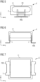
- Figure 5 illustrates a cross-section in a view parallel to the horizontal y direction of a capacitor C.
- the terminals T comprise two legs that are electrically and mechanically connected at a location within the housing H and that are electrically and mechanically connected at the bottom side, specifically at the flat bottom side FBS, making the capacitor C compliant with SMT processes.
- Figure 6 shows a cross-section parallel to a horizontal direction x.
- the terminals T1, T2 are L-shaped.
- Figure 5 and Figure 6 clearly show that the position of the capacitance element CE within the housing H is off-center. Specifically, the center of the capacitance element CE is arranged at a higher position compared to the center of the housing H of the capacitor C. Thus, the length of the terminals T is increased and thermal resistance to the flat bottom sides is also increased.
- Figure 6 shows a bottom view of the capacitor C. This means that the perspective is on the flat bottom sides FBS.
- the flat bottom sides FBS can be considered as comprising a rectangular shape and two added smaller rectangles attached at the distal ends of the main rectangular patch of the terminals T.
- Figure 8 shows a perspective view of a capacitor C.
- the width W in the horizontal direction x can be 28.5 mm.
- the length in the horizontal direction y can be 31.5 mm.
- the vertical height of the housing H can be 13 mm.
- the overall height of the capacitor C including the vertical dimensions of the terminals H can be 15 mm.
- the distance between the two terminals P can be 27.5 mm.
- FIG 9 shows a perspective view of the housing H of the capacitor.
- the housing H is a double wall case.
- the housing H comprises an inner wall IW and an outer wall OW.
- the inner wall IW faces towards a cavity which is enclosed by the housing H and in which the capacitor element CE is arranged.
- the outer wall OW faces away from the cavity which is enclosed by the housing H.
- the inner wall IW and the outer wall OW do not abut each other. Instead, the inner wall IW and the outer wall OW are separated by a gap G.
- the gap G may be filled with air or with another thermally insulating material.
- the housing H is a double wall case, it provides a very high thermal insulation of the capacitor element CE from the environment of the housing H.
- the capacitor and the methods and uses are not limited to the properties described above.
- the capacitor can comprise further elements such as temperature sensors, heat shields, mechanical or electrical protection elements, e.g. for protecting the capacitor against over-voltages.
- the terminals specifically the flat bottom sides of the terminals, can comprise additional materials, e.g. solder, for enhancing the solder process. Uses other than EMI reduction or in a DC-link component are also possible. Specifically, it is possible to use the capacitor as a short-term energy storage.
- the capacitor can be used with corresponding capacitors to establish a capacitor array for increased capacitance or for increased voltage resistance. Then, the capacitors can be arranged in a series connection or in a parallel connection or both.
Landscapes
- Engineering & Computer Science (AREA)
- Power Engineering (AREA)
- Microelectronics & Electronic Packaging (AREA)
- Manufacturing & Machinery (AREA)
- Fixed Capacitors And Capacitor Manufacturing Machines (AREA)
Applications Claiming Priority (3)
| Application Number | Priority Date | Filing Date | Title |
|---|---|---|---|
| DE102022103760.6A DE102022103760A1 (de) | 2022-02-17 | 2022-02-17 | Kondensator, Verfahren zur Herstellung und Verwendung |
| PCT/EP2023/053922 WO2023156540A1 (fr) | 2022-02-17 | 2023-02-16 | Condensateur, son procédé de fabrication et son utilisation |
| EP23707655.9A EP4479991A1 (fr) | 2022-02-17 | 2023-02-16 | Condensateur, son procédé de fabrication et son utilisation |
Related Parent Applications (1)
| Application Number | Title | Priority Date | Filing Date |
|---|---|---|---|
| EP23707655.9A Division EP4479991A1 (fr) | 2022-02-17 | 2023-02-16 | Condensateur, son procédé de fabrication et son utilisation |
Publications (2)
| Publication Number | Publication Date |
|---|---|
| EP4492416A2 true EP4492416A2 (fr) | 2025-01-15 |
| EP4492416A3 EP4492416A3 (fr) | 2026-02-11 |
Family
ID=85384281
Family Applications (2)
| Application Number | Title | Priority Date | Filing Date |
|---|---|---|---|
| EP24216065.3A Pending EP4492416A3 (fr) | 2022-02-17 | 2023-02-16 | Condensateur, procédé de fabrication et utilisation |
| EP23707655.9A Pending EP4479991A1 (fr) | 2022-02-17 | 2023-02-16 | Condensateur, son procédé de fabrication et son utilisation |
Family Applications After (1)
| Application Number | Title | Priority Date | Filing Date |
|---|---|---|---|
| EP23707655.9A Pending EP4479991A1 (fr) | 2022-02-17 | 2023-02-16 | Condensateur, son procédé de fabrication et son utilisation |
Country Status (5)
| Country | Link |
|---|---|
| US (1) | US20250157740A1 (fr) |
| EP (2) | EP4492416A3 (fr) |
| JP (2) | JP2025506529A (fr) |
| DE (1) | DE102022103760A1 (fr) |
| WO (1) | WO2023156540A1 (fr) |
Family Cites Families (30)
| Publication number | Priority date | Publication date | Assignee | Title |
|---|---|---|---|---|
| US3034198A (en) * | 1957-09-24 | 1962-05-15 | Illinois Tool Works | Electronic assembly |
| DE3466121D1 (en) * | 1983-06-03 | 1987-10-15 | Wolfgang Westermann | Plastic foil-wound capacitor |
| JPH02113512A (ja) * | 1988-10-21 | 1990-04-25 | Matsushita Electric Ind Co Ltd | フィルムコンデンサ |
| JPH03293709A (ja) | 1990-04-11 | 1991-12-25 | Nippon Chemicon Corp | チップ型フィルムコンデンサ |
| JPH06104140A (ja) * | 1992-08-05 | 1994-04-15 | Rubikon Denshi Kk | チップ型フィルムコンデンサおよびその製造方法 |
| JP2000323352A (ja) * | 1999-05-06 | 2000-11-24 | Nichicon Corp | 電子部品 |
| US6356431B1 (en) * | 2001-03-26 | 2002-03-12 | Ming Chang Lin | Connection pins of a capacitor |
| AU2002326844A1 (en) * | 2001-09-07 | 2003-03-24 | Dearborn Electronics Inc | Film capacitor for high temperature applications |
| JP4201623B2 (ja) | 2002-11-19 | 2008-12-24 | 三洋電機株式会社 | 固体電解コンデンサ |
| JP4747560B2 (ja) * | 2004-11-17 | 2011-08-17 | パナソニック株式会社 | フィルムコンデンサおよびその製造方法 |
| WO2008108089A1 (fr) * | 2007-03-08 | 2008-09-12 | Panasonic Corporation | Condensateur à boîtier moulé et son procédé d'utilisation |
| US20080232026A1 (en) * | 2007-03-20 | 2008-09-25 | Ward Terence G | Thin film capacitor and methods of making same |
| US7864506B2 (en) * | 2007-11-30 | 2011-01-04 | Hamilton Sundstrand Corporation | System and method of film capacitor cooling |
| US8018712B2 (en) * | 2008-03-13 | 2011-09-13 | Nuintek Co., Ltd. | Bus-bar for jointing capacitor |
| KR101034063B1 (ko) * | 2008-11-24 | 2011-05-12 | 현대자동차주식회사 | 필름커패시터 |
| KR20120097753A (ko) * | 2011-02-25 | 2012-09-05 | 주식회사 뉴인텍 | 커패시터용 함침탱크 |
| JP6122641B2 (ja) * | 2013-01-08 | 2017-04-26 | 岡谷電機産業株式会社 | ケース外装型コンデンサ |
| JP6393026B2 (ja) * | 2013-08-09 | 2018-09-19 | 日立エーアイシー株式会社 | 金属化フィルムコンデンサ |
| US9960698B2 (en) * | 2014-12-22 | 2018-05-01 | Flex Power Control, Inc. | Reliable AC-DC power converter with high voltage DC link |
| EP3089179B1 (fr) * | 2015-04-29 | 2020-10-21 | General Electric Technology GmbH | Boîtier d'équipement électrique comprenant une paroi double usage pour la réduction de bruit |
| WO2018100852A1 (fr) * | 2016-11-29 | 2018-06-07 | パナソニックIpマネジメント株式会社 | Condensateur |
| DE102018119216B4 (de) * | 2018-08-07 | 2020-07-23 | Tdk Electronics Ag | Gehäuse für eine elektronische Komponente mit einem Innenbehälter und einer Außenumhüllung |
| JP2020035786A (ja) * | 2018-08-27 | 2020-03-05 | トヨタ自動車株式会社 | コンデンサ装置の製造方法 |
| CN113196427B (zh) * | 2018-12-25 | 2023-10-13 | 松下知识产权经营株式会社 | 电容器 |
| US11282640B2 (en) * | 2019-04-12 | 2022-03-22 | Karma Automotive Llc | DC link capacitor cooling system |
| JP6867432B2 (ja) * | 2019-05-09 | 2021-04-28 | 三菱電機株式会社 | 電力変換装置 |
| CN213340098U (zh) * | 2020-10-10 | 2021-06-01 | 南通百正电子新材料股份有限公司 | 一种易散热的聚丙烯薄膜电容器 |
| CN213716723U (zh) * | 2020-11-18 | 2021-07-16 | 东莞市普隆电子有限公司 | 一种直流吸收保护电容器 |
| WO2022212640A1 (fr) * | 2021-03-31 | 2022-10-06 | Kemet Electronics Corporation | Composant électronique ayant une résistance à la chaleur améliorée |
| CN215578214U (zh) * | 2021-05-11 | 2022-01-18 | 许昌市国源电气有限公司 | 一种防爆电容器 |
-
2022
- 2022-02-17 DE DE102022103760.6A patent/DE102022103760A1/de active Pending
-
2023
- 2023-02-16 US US18/838,524 patent/US20250157740A1/en active Pending
- 2023-02-16 EP EP24216065.3A patent/EP4492416A3/fr active Pending
- 2023-02-16 WO PCT/EP2023/053922 patent/WO2023156540A1/fr not_active Ceased
- 2023-02-16 EP EP23707655.9A patent/EP4479991A1/fr active Pending
- 2023-02-16 JP JP2024548558A patent/JP2025506529A/ja active Pending
-
2025
- 2025-09-16 JP JP2025152973A patent/JP2025179848A/ja active Pending
Also Published As
| Publication number | Publication date |
|---|---|
| JP2025179848A (ja) | 2025-12-10 |
| DE102022103760A1 (de) | 2023-08-17 |
| JP2025506529A (ja) | 2025-03-11 |
| US20250157740A1 (en) | 2025-05-15 |
| WO2023156540A1 (fr) | 2023-08-24 |
| EP4479991A1 (fr) | 2024-12-25 |
| EP4492416A3 (fr) | 2026-02-11 |
Similar Documents
| Publication | Publication Date | Title |
|---|---|---|
| CN1714415B (zh) | 金属化膜电容器 | |
| US7031141B2 (en) | Solid electrolytic capacitor and electric circuit | |
| US7911765B2 (en) | Metalized film capacitor, case mold type capacitor using the same, inverter circuit, and vehicle drive motor drive circuit | |
| JP5953246B2 (ja) | 電力変換装置 | |
| US10692655B2 (en) | Filter component for filtering an interference signal | |
| WO2010111575A2 (fr) | Condensateur en céramique multicouche à grille de connexion avec esl et esr réduits | |
| JP5239989B2 (ja) | ケースモールド型コンデンサ | |
| KR20140007497A (ko) | 커패시터 | |
| JP6305731B2 (ja) | ケースモールド型コンデンサおよびその製造方法 | |
| US9679701B2 (en) | Tantalum capacitor | |
| EP4492416A2 (fr) | Condensateur, procédé de fabrication et utilisation | |
| CN117321714A (zh) | 耐热性改进的电子元件 | |
| CN116612986A (zh) | 电容器、制造方法和用途 | |
| CN118633135A (zh) | 电容器 | |
| JP2009277827A (ja) | コンデンサ | |
| JP4803749B2 (ja) | 金属化フィルムコンデンサ | |
| CN212676110U (zh) | 低电感电容器和电容器组 | |
| KR102809010B1 (ko) | 필름 커패시터 모듈 | |
| US12387860B2 (en) | Electrical component comprising an electrical resistor | |
| Kerrigan et al. | Film capacitor thermal strategies increase power density | |
| WO2017150151A1 (fr) | Condensateur à film | |
| JPH06333789A (ja) | 低インピーダンス四端子型固体電解コンデンサ | |
| JPS6158227A (ja) | チツプ形電解コンデンサ | |
| Kaiser | Capacitors-various dielectrics and their applications | |
| CN115172047A (zh) | 电容器芯子、电容器及制造方法、使用电容器的设备 |
Legal Events
| Date | Code | Title | Description |
|---|---|---|---|
| PUAI | Public reference made under article 153(3) epc to a published international application that has entered the european phase |
Free format text: ORIGINAL CODE: 0009012 |
|
| STAA | Information on the status of an ep patent application or granted ep patent |
Free format text: STATUS: REQUEST FOR EXAMINATION WAS MADE |
|
| 17P | Request for examination filed |
Effective date: 20241128 |
|
| AC | Divisional application: reference to earlier application |
Ref document number: 4479991 Country of ref document: EP Kind code of ref document: P |
|
| AK | Designated contracting states |
Kind code of ref document: A2 Designated state(s): AL AT BE BG CH CY CZ DE DK EE ES FI FR GB GR HR HU IE IS IT LI LT LU LV MC ME MK MT NL NO PL PT RO RS SE SI SK SM TR |
|
| REG | Reference to a national code |
Ref country code: DE Ref legal event code: R079 Free format text: PREVIOUS MAIN CLASS: H01G0002100000 Ipc: H01G0002060000 |
|
| RIC1 | Information provided on ipc code assigned before grant |
Ipc: H01G 2/06 20060101AFI20250820BHEP Ipc: H01G 4/32 20060101ALI20250820BHEP Ipc: H01G 2/08 20060101ALI20250820BHEP Ipc: H01G 4/224 20060101ALI20250820BHEP Ipc: H01G 4/232 20060101ALI20250820BHEP Ipc: H01G 4/18 20060101ALI20250820BHEP Ipc: H01G 4/40 20060101ALI20250820BHEP Ipc: H01G 2/10 20060101ALN20250820BHEP |
|
| PUAL | Search report despatched |
Free format text: ORIGINAL CODE: 0009013 |
|
| AK | Designated contracting states |
Kind code of ref document: A3 Designated state(s): AL AT BE BG CH CY CZ DE DK EE ES FI FR GB GR HR HU IE IS IT LI LT LU LV MC ME MK MT NL NO PL PT RO RS SE SI SK SM TR |
|
| RIC1 | Information provided on ipc code assigned before grant |
Ipc: H01G 2/06 20060101AFI20260108BHEP Ipc: H01G 4/32 20060101ALI20260108BHEP Ipc: H01G 2/08 20060101ALI20260108BHEP Ipc: H01G 4/224 20060101ALI20260108BHEP Ipc: H01G 4/232 20060101ALI20260108BHEP Ipc: H01G 4/18 20060101ALI20260108BHEP Ipc: H01G 4/40 20060101ALI20260108BHEP Ipc: H01G 2/10 20060101ALN20260108BHEP |