EP4492570A1 - Agencement de guide d'ondes et dispositif de rayonnement et/ou de réception d'ondes - Google Patents
Agencement de guide d'ondes et dispositif de rayonnement et/ou de réception d'ondes Download PDFInfo
- Publication number
- EP4492570A1 EP4492570A1 EP23184492.9A EP23184492A EP4492570A1 EP 4492570 A1 EP4492570 A1 EP 4492570A1 EP 23184492 A EP23184492 A EP 23184492A EP 4492570 A1 EP4492570 A1 EP 4492570A1
- Authority
- EP
- European Patent Office
- Prior art keywords
- metallic layer
- dielectric substrate
- top surface
- magnetic conducting
- conducting structures
- Prior art date
- Legal status (The legal status is an assumption and is not a legal conclusion. Google has not performed a legal analysis and makes no representation as to the accuracy of the status listed.)
- Pending
Links
Images



Classifications
-
- H—ELECTRICITY
- H01—ELECTRIC ELEMENTS
- H01Q—ANTENNAS, i.e. RADIO AERIALS
- H01Q1/00—Details of, or arrangements associated with, antennas
- H01Q1/27—Adaptation for use in or on movable bodies
- H01Q1/32—Adaptation for use in or on road or rail vehicles
- H01Q1/3208—Adaptation for use in or on road or rail vehicles characterised by the application wherein the antenna is used
- H01Q1/3233—Adaptation for use in or on road or rail vehicles characterised by the application wherein the antenna is used particular used as part of a sensor or in a security system, e.g. for automotive radar, navigation systems
-
- H—ELECTRICITY
- H01—ELECTRIC ELEMENTS
- H01P—WAVEGUIDES; RESONATORS, LINES, OR OTHER DEVICES OF THE WAVEGUIDE TYPE
- H01P1/00—Auxiliary devices
- H01P1/20—Frequency-selective devices, e.g. filters
- H01P1/213—Frequency-selective devices, e.g. filters combining or separating two or more different frequencies
- H01P1/2135—Frequency-selective devices, e.g. filters combining or separating two or more different frequencies using strip line filters
-
- H—ELECTRICITY
- H01—ELECTRIC ELEMENTS
- H01P—WAVEGUIDES; RESONATORS, LINES, OR OTHER DEVICES OF THE WAVEGUIDE TYPE
- H01P3/00—Waveguides; Transmission lines of the waveguide type
- H01P3/02—Waveguides; Transmission lines of the waveguide type with two longitudinal conductors
- H01P3/08—Microstrips; Strip lines
- H01P3/085—Triplate lines
- H01P3/087—Suspended triplate lines
-
- H—ELECTRICITY
- H01—ELECTRIC ELEMENTS
- H01P—WAVEGUIDES; RESONATORS, LINES, OR OTHER DEVICES OF THE WAVEGUIDE TYPE
- H01P5/00—Coupling devices of the waveguide type
- H01P5/02—Coupling devices of the waveguide type with invariable factor of coupling
- H01P5/022—Transitions between lines of the same kind and shape, but with different dimensions
- H01P5/028—Transitions between lines of the same kind and shape, but with different dimensions between strip lines
-
- H—ELECTRICITY
- H01—ELECTRIC ELEMENTS
- H01Q—ANTENNAS, i.e. RADIO AERIALS
- H01Q21/00—Antenna arrays or systems
- H01Q21/0006—Particular feeding systems
- H01Q21/0037—Particular feeding systems linear waveguide fed arrays
- H01Q21/0043—Slotted waveguides
-
- H—ELECTRICITY
- H01—ELECTRIC ELEMENTS
- H01Q—ANTENNAS, i.e. RADIO AERIALS
- H01Q21/00—Antenna arrays or systems
- H01Q21/0006—Particular feeding systems
- H01Q21/0037—Particular feeding systems linear waveguide fed arrays
- H01Q21/0043—Slotted waveguides
- H01Q21/005—Slotted waveguides arrays
-
- H—ELECTRICITY
- H01—ELECTRIC ELEMENTS
- H01Q—ANTENNAS, i.e. RADIO AERIALS
- H01Q21/00—Antenna arrays or systems
- H01Q21/0006—Particular feeding systems
- H01Q21/0075—Stripline fed arrays
- H01Q21/0081—Stripline fed arrays using suspended striplines
Definitions
- the present invention relates to a waveguide arrangement and to a wave radiating and/or receiving device.
- patch antennas were considered as the most suitable radiating elements due to small bandwidth requirement.
- Known patch antennas are related to narrow bands, wherein an increase of the bandwidth may require increasing the substrate thickness or introducing parasitic elements.
- Automotive radar sensors of the next generation can face spatial resolution requirements that translate to operational bandwidths of 4 GHz to 5 GHz and therefore a consideration of the limitations associated with the planar patch antennas to achieving high RF performance requirements for the next generation radars.
- waveguide antennas have lower loss and better overall efficiency and waveguides are known and common to carry electromagnetic waves from one point to the other point through a guided medium without undesired leakage.
- the guiding medium can be air or free space for a classical hollow waveguide.
- the metallic walls of typical hollow waveguides can prevent the electromagnetic wave from spreading and bound it to travel in a specified direction thereby reducing the transmission losses.
- Generally known waveguides can be categorized into rectangular and circular waveguides and can have slots on their surface for radiating the electromagnetic waves.
- the electromagnetic wave can be fed through an excitation source from the transmission side and exit towards the receiving side with a similar excitation source, which can be referred to as a waveguide launcher. It is possible to emit the electromagnetic waves from the waveguide in several ways, wherein a most common way is to provide slots in the wall of the waveguide.
- Several antennas can be arranged to achieve an antenna array for radar sensor devices, wherein such an arrangement would also require a feed network to transfer the electromagnetic wave from the source to the antenna element, which can be deployed in an underlying layer arrangement to reach a smaller antenna aperture, by avoiding intersections of the routing lines, and gain antenna design freedom.
- a top layer can have a radiating unit cell and a bottom layer can have a feed network.
- a waveguide antenna Since one of the major constraints of a waveguide antenna can be its size the application of such an antenna as a large antenna array required in for example an imaging radar, the antenna may become bulky and thicker resulting in the increase of the sensor size and weight. As a consequence it is desirable to provide a multilayer waveguide arrangement with metasurfaces proposed to counteract the above mentioned drawbacks.
- This multilayer waveguide arrangement can, for example, be based on gap waveguide technology.
- Such a waveguide can use a coaxial line mode of propagation and artificial magnetic conductor (AMC) structures to trap the electromagnetic waves inside a predefined region, wherein an inner conductor for feeding electromagnetic waves in the predefined region can be realized by support structures to hold the conductor.
- AMC artificial magnetic conductor
- US 2011/0181373 A1 describes waveguides and transmission lines in gap waveguide structures between parallel conducting surfaces for microwave devices.
- the present invention pertains to a waveguide arrangement according to claim 1 and to a wave radiating and/or receiving device according to claim 10.
- the waveguide arrangement comprises a dielectric substrate having a flat top surface and a flat bottom surface opposite the top surface; at least one stripline having an electrically conductive material, wherein the stripline is arranged on the flat top surface and/or on the flat bottom surface in a predefined region for guiding an electromagnetic wave along; a first metallic layer having a flat bottom surface and magnetic conducting structures which are arranged in a first predefined pattern on the flat bottom surface, wherein the first metallic layer is arranged such above the dielectric substrate that the magnetic conducting structures are directed towards the dielectric substrate and its flat top surface; a second metallic layer having a flat top surface and magnetic conducting structures which are arranged in a second predefined pattern on the flat top surface, wherein the second metallic layer is arranged such below the dielectric substrate that the magnetic conducting structures are directed towards the dielectric substrate and its flat bottom surface, wherein in a projection perpendicular on the flat top surface and/or on the flat bottom surface of the dielectric substrate the magnetic conducting structures are arranged laterally beside the at least one stripline.
- the waveguide arrangement according to the invention it is possible to omit further construction elements or minimize their application and/or number such as holders for supporting a conductor element for the electromagnetic waves (for example the stripline) which can usually be distributed periodically over long transmission lines (geometry of the stripline) and which usually may cause undesirable relatively high reflection coefficients and reduce the operating frequency bandwidth.
- the waveguide arrangement according to the invention can provide straight stripline geometries which have less sensitivity to assembly tolerances especially for curved transmission lines with unevenly distributed supporting holders.
- the first and/or second metallic layers can be solid metallic layers or non-metallic layers covered with a metallic coating.
- Examples of applicable metals include brass, copper or aluminum.
- the dielectric substrate can represent an inner layer in a sandwiched waveguide arrangement (for example of a multilayer waveguide MLWG) and can be designed using a dielectric material with a stripline acting as an inner conductor for electromagnetic waves inside the sandwiched component and which does not require any holders because the stripline is fixed by the substrate.
- a sandwiched waveguide arrangement for example of a multilayer waveguide MLWG
- the stripline has a top part being arranged on the flat top surface of the dielectric substrate and a bottom part being arranged on the flat bottom surface of the dielectric substrate, wherein in a projection perpendicular on the flat top surface the top part and the bottom part overlap each other fully or partly.
- the waveguide arrangement at least one via in the dielectric substrate electrically connects the top stripline with the bottom stripline. Further vias can be placed at specific locations to avoid any conductive imbalances between the top and bottom stripline (the top part and bottom part of the stripline).
- a predefined gap is defined between the magnetic conducting structures by the thickness of the dielectric substrate or any kind of further metallization or any kind of additional air gaps.
- a further predefined gap remains between the magnetic conducting structures and the dielectric substrate.
- the magnetic conducting structures may be arranged in contact with the dielectric substrate layer or may be arranged to form an air gap.
- the antenna/waveguide arrangement may be manufactured with the intent of having all magnetic conducting structures to contact the dielectric substrate, manufacturing tolerances may result in one or more, or even all, of the magnetic conducting structures being arranged with an air gap that results in no electrical contact.
- the first predefined pattern and the second predefined pattern can be identical.
- the magnetic conducting structures are arranged in a predefined periodicity with predefined distances between each other and with predefined distances to the stripline in dependence on the wavelength of the electromagnetic wave to be guided by the stripline and wherein the magnetic conducting structures have a predefined height.
- the predefined dimensions can be scaled for different wavelengths, for example if particular dimensions for a predefined wavelength are known then the resulting dimensions can be scaled for another wavelength based on the factor of difference between the two wavelengths.
- the first metallic layer and/or the second metallic layer has at least one opening for entering or exiting a radiation to or from an interior of the waveguide arrangement, wherein the interior is formed between the first metallic layer and/or the second metallic layer and the dielectric substate.
- the interior is further formed between the magnetic conducting structures and the stripline can be located within the interior which can be hollow or filled by a gaseous or solid material.
- the wave radiating and/or receiving device comprises at least one waveguide arrangement according to the invention; and an antenna block which is placed on the first metallic layer, for example on a top side, or on the second metallic layer, for example on a bottom side, and on an opening for entering or exiting a radiation to or from an interior of the waveguide arrangement to or from the antenna block.
- the antenna block comprises a dielectric substrate having a flat top surface and a flat bottom surface opposite the top surface; at least one stripline having an electrically conductive material, wherein the stripline is arranged on the flat top surface and/or on the flat bottom surface in a predefined region for guiding an electromagnetic wave along; a first metallic layer having a flat bottom surface and magnetic conducting structures which are arranged in a predefined pattern on the flat bottom surface, wherein the first metallic layer is arranged such above the dielectric substrate that the magnetic conducting structures are directed towards the dielectric substrate and its flat top surface; a second metallic layer having a flat top surface and magnetic conducting structures which are arranged in a predefined pattern on the flat top surface, wherein the second metallic layer is arranged such below the dielectric substrate that the magnetic conducting structures are directed towards the dielectric substrate and its flat bottom surface, wherein in a projection perpendicular on the flat top surface and/or on the flat bottom surface of the dielectric substrate the magnetic conducting structures are arranged laterally
- the antenna block comprises a bottom opening for exiting or entering the electromagnetic wave to the waveguide arrangement and which is placed on an opening of the first metallic layer or of the second metallic layer of the waveguide arrangement exiting or entering the electromagnetic wave from the waveguide arrangement.
- the first metallic layer of the antenna block has at least one radiation opening for exiting or entering the electromagnetic wave from the exterior to the interior of the antenna block or vice versa.
- the antenna block has several radiation openings arranged in a predefined pattern.
- the pattern of magnetic conducting structures laterally fully surrounds the stripline.
- the antenna block and the waveguide arrangement are each provided as unit cells.
- the wave radiating and/or receiving device it comprises at least a first array of antenna blocks and waveguide arrangements and a feed distribution on a circuit board which is arranged between the waveguide arrangements and a radar chip device.
- the magnetic conducting structures of the first and/or second metallic layer form a textured surface with thicker and thiner sections in height.
- the magnetic conductive structure can be realized by a textured surface (of the metallic layer(s) or of the magnetic conductive structure itself).
- a difference in height between the thicker and thiner sections of the textured surface is less than ⁇ /5, preferably less than ⁇ /9 and most preferably less than ⁇ /12.
- ⁇ is the operating free space wavelength.
- the wave radiating and/or receiving device is a radar or part of a radar device or which is used by a radar, for example in or for a vehicle, or by any radio emitting device.
- the mentioned wave radiating and/or receiving device can be used for radiating and/or receiving of electromagnetic radiation and represents a subwavelength thin multi-layer gap waveguide with a sandwiched conducting stripline.
- the wave radiating and/or receiving device can also be specified by the features and advantages of the waveguide arrangement and vice versa.
- the feedlines can be included/integrated in the upper three layers consisting of the radiator slots 21.
- the total number of layers is thereby reduced to three metallic layers, which results in reduced component costs.
- Fig. 1 shows a multilayer waveguide arrangement according to the prior art.
- the multilayer waveguide 1a has a top metallic layer A, a bottom metallic layer B and an inner metallic layer IN which is sandwiched between the top metallic layer A and the bottom metallic layer B with a predefined height between both metallic layers.
- artificial magnetic conductors AMCs for example as high impedance structures are arranged at a bottom face of the top metallic layer A and at a top face of the bottom metallic layer B and which are connected to the corresponding layer. Further, the artificial magnetic conductors AMCs can extend towards the inner metallic layer IN.
- a hollow is provided in a central region of the sandwiched arrangement 1a and of the inner metallic layer IN a hollow is provided and a conductor C for electromagnetic waves placed in this hollow and holders H are arranged between the conductor C and the inner metallic layer IN at predefined distances between the holders such that the conductor C can be held at a further predefined distance towards the inner metallic layer IN.
- a field of the electromagnetic wave can be trapped inside the arrangement of AMCs and in the hollow region.
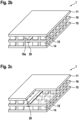
- Figures 2a , 2b and 2c show different views of a waveguide arrangement according to an embodiment of the invention.
- Fig. 2a shows a cross sectional view to the longitudinal extent of the stripline 20 and Fig. 2b shows a perspective view on an exterior of the sandwiched waveguide arrangement 1.
- the waveguide arrangement 1 comprises a dielectric substrate 19 having a flat top surface 19a and a flat bottom surface 19b opposite the top surface 19a, as shown in Fig. 2b .
- a stripline 20 having an electrically conductive material is arranged on the flat top surface 19a and on the flat bottom surface 19b in a predefined region for guiding an electromagnetic wave along, in particular at a hollow central region, namely the interior 18.
- a first metallic layer 11 has a flat bottom surface 11b and magnetic conducting structures 12, in particular artificial magnetic conductors, which are arranged in a predefined pattern on the flat bottom surface 11b, wherein the first metallic layer 11 is arranged such above the dielectric substrate 19 that the magnetic conducting structures 12 are directed towards the dielectric substrate 19 and its flat top surface 19a.
- a second metallic layer 15 has a flat top surface 15a and magnetic conducting structures 14 which are arranged in a predefined pattern on the flat top surface 15a, wherein the second metallic layer 15 is arranged such below the dielectric substrate 19 that the magnetic conducting structures 14 are directed towards the dielectric substrate 19 and its flat bottom surface 19b, wherein in a projection perpendicular on the flat top surface 19a and/or on the flat bottom surface 19b of the dielectric substrate 19 the magnetic conducting structures (12, 14) are arranged laterally beside the at least one stripline 20.
- the stripline 20 has a top part 20a being arranged on the flat top surface 19a of the dielectric substrate 19 and a bottom part 20b being arranged on the flat bottom surface 19b of the dielectric substrate 19, wherein in a projection perpendicular on the flat top surface 19a the top part 20a and the bottom part 20b overlap each other fully or partly.
- a predefined gap GP remains between the magnetic conducting structures (12, 14) and the dielectric substrate 19.
- the stripline 20 can represent a conductor along which the electromagnetic wave can propagate.
- the wave conducting element in particular the stripline 20
- the waveguide arrangement 1 can represent a multilayered waveguide with a stripline line 20 on the dielectric substrate 19 such that it is sandwiched between the metallic layers 11 and 15, wherein magnetic conducting structures, for example as pins, can be arranged between the dielectric substrate and the metallic layers respectively and in a predefined pattern around the interior (hollow) region 18 in order to trap the electromagnetic fields therein and guide the electromagnetic wave along the longitudinal direction of the stripline 20.
- the pins height and the periodicity of the AMCs (12, 14) can be operating wavelength dependent.
- the pins (12, 14) can function as a barrier or fence to prevent the electromagnetic wave from propagating in the directions other than the desired one.
- the dielectric substrate 19 allows the conductor 20 to float without holding structures and the thickness of the substrate can be lowered when compared to the prior art allowing the fields to be more concentrated in the hollow (interior) region, for example the substrate 19 can be in the range between 35 to 128 ⁇ m.
- the thickness of the whole multilayer element is mainly limited due to the pin height (height of the magnetic conducting structures (pins) in direction between the dielectric substrate and the first or second metallic layer), which is typically, i.e., ⁇ 0 /10 (where ⁇ 0 is the operating free space wavelength).
- a waveguide usually has three layers stacked in such a way that the top and bottom metallic layers are symmetric around the inner dielectric layer.
- the pin height can be less than ⁇ /5, ⁇ /7, ⁇ /9 or preferable less than ⁇ /12.
- Fig. 2c shows a view similar to Fig. 2b with a cut through the first metallic layer 11 in order to show the periodic arrangement of the magnetic conducting structures 12 along the stripline 20, wherein the magnetic conducting structures 12 and 14 can be arranged with a predefined periodicity what means in a repeating number or pattern along a width and length of the metallic layers 11 and 15 with predefined distances between each other and towards the stripline and/or towards the edges of the particular metallic layer (11, 15).
- two parallel rows of magnetic conducting structures 12 can be arranged on each lateral side of the stripline 20 in order to provide a predefined fence function for the fields of the electromagnetic wave in lateral directions.
- the magnetic conducting structures 12 and 14 can laterally surround the stripline on each lateral side with a predefined pattern and hold the electromagnetic fields of the electromagnetic wave trapped inside the interior region 18 ( Fig. 2a ).
- the predefined periodicity with corresponding distances depends on the wavelength which is guided by the stripline.
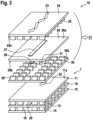
- Fig. 3 shows a wave radiating and/or receiving device in an exploded view according to an embodiment of the invention.
- the waveguide arrangement 1 as mentioned, for example, in Figures 2a - 2c is shown in a sandwiched form in the bottom region of Fig. 3 .
- a slot 32 is shown for exiting the electromagnetic wave from the waveguide arrangement 1 through the slot opening 32 at this predefined location.
- an antenna block 21 is shown in exploded view such that the layers and elements can be seen in separated positions but in real the antenna block 21 is provided in compact form as shown in Fig. 4 .
- the antenna block 21 comprises a (further) dielectric substrate 26 having a flat top surface 26a and a flat bottom surface 26b opposite the top surface 26a; at least one (further) stripline 27 having an electrically conductive material, wherein the stripline 27 is arranged on the flat top surface 26a and/or on the flat bottom surface 26b in a predefined region for guiding an electromagnetic wave along; a (further) first metallic layer 24 having a flat bottom surface 24b and magnetic conducting structures 25 which are arranged in a predefined pattern on the flat bottom surface 24b, wherein the first metallic layer 24 is arranged such above the dielectric substrate 26 that the magnetic conducting structures 25 are directed towards the dielectric substrate 26 and its flat top surface 26a; a (further) second metallic layer 30 having a flat top surface 30a and magnetic conducting structures 29 which are arranged in a predefined pattern on the flat top surface 30a, wherein the second metallic layer 30 is arranged such below the dielectric substrate 26 that the magnetic conducting structures 29 are directed towards the dielectric substrate 26 and its
- the sandwiched structure of the antenna block 21 can mostly correpond to the sandwiched structure of the waveguide arrangement 1, for example with regard to sizes of components and arrangements of magnetic conducting structures like numbers and distances between them for influencing the same wavelength range as the waveguide arrangement 1.
- the electromagnetic wave can exit the waveguide arrangement 1 from the slot 32 and enter the antenna block 21 through another slot 31 in the second metallic layer 30 and can be propagated through the antenna block 21 along the further stripline 27 which is arranged in a hollow interior of the antenna block 21.
- the further stripline 27 can extend along a predefined path on one or both sides of the dielectric substrate 26 to guide the electromagnetic wave and be surrounded from lateral and longitudinal sides by magnetic conducting structures 25 (and/or 29).
- the further stripline 27 does in this example not reach the edge of the dielectric substrate 26 as this can be the case for the stripline of the waveguide arrangement 1 but is rather faced with further magnetic conducting structures 25 (and/or 29) in this longitudinal direction in order to keep the electromagnetic wave trapped inside the interior of the antanna block 21 also along this longitudinal direction.
- the stripline can have a top part 27 facing a radiating side of the substrate 26 and a bottom part 28 facing a non-radiating side of the substrate 26, wherein in perspective a top view both bottom and top parts 27 and 28 can overlap each other.
- the magnetic conducting structures 25 (and/or 29) can comprise metal.
- the first metallic layer 24 of the antenna block 21 can have at least one radiation opening 23 (or several as shown in Fig. 3 ) for exiting or entering the electromagnetic wave from the exterior to the interior of the antenna block 21 or vice versa.
- the several radiation openings 23 can be arranged in a predefined pattern for achieving a predefined radiation pattern. The radiation can be radiated through the slots 23 in a desired direction and/or received through the same slots and also radiated through the slot 31 and 32 to the waveguide arrangement 1.
- Fig. 4 shows the wave radiating and/or receiving device from Fig. 3 in a compact view.
- the antenna block 21 can be placed on the first metallic layer 11 and the antenna block 21 can be designed with the slots 23 to radiate an electromagnetic wave in a particular direction to achieve a desired field of view.
- the waveguide arrangement 1 can be designed to transmit an electromagnetic wave through the stripline(s) as feedlines from the launcher/excitation source to a radiator (not shown).
- six layers of the antenna block and of the waveguide arrangement 1 together can form a unit cell radiator, that can be used in several configurations to achieve a desired radiation pattern.
- the shape and dimension of the slot 23 can be adapted to the desired radiating and receiving properties.
- Fig. 5 shows a wave radiating and/or receiving device according to another embodiment of the invention.
- the wave radiating and/or receiving device 10 is shown in a top view on a printed circuit board PCB having two arrays of antenna blocks A1 and A2, wherein for each array an imprint 36 of connections and of circuits (IC) 37 can be provided on the circuit board PCB, for example imprints for the circuits on the underlying RF substrate layer of the PCB.
- a metallized feedline layer 34 can be provided on the top side of the PCB 35 .
- Feed lines 34 guide the electromagnetic waves to the antenna blocks 21 and the electromagnetic wave can be radiated through the pattern of slots 33.
- the slots 33 may be incorporated in a common top antenna layer.
- a communication line 38 can be provided between the two imprint regions (36, 37) of the arrays.
- the wave radiating and/or receiving device 10 can be used, for example, for an imaging radar and/or driverless applications but also other radiation and receiving applications are possible.
- Fig. 6 shows a view of a waveguide arrangement according to a further embodiment of the invention.
- Fig. 6 shows a side view to the sandwiched arrangement of the waveguide arrangement 1 with vias VA at predefined positions and distances in the stripline 20.
- the waveguide arrangement 1 comprises a dielectric substrate 19 having a flat top surface and a flat bottom surface opposite the top surface and the vias VA in the dielectric substrate 19 electrically connect the top part 20a and the bottom part 20b of the stripline 20.
Landscapes
- Engineering & Computer Science (AREA)
- Computer Security & Cryptography (AREA)
- Radar, Positioning & Navigation (AREA)
- Remote Sensing (AREA)
- Waveguide Aerials (AREA)
Priority Applications (3)
| Application Number | Priority Date | Filing Date | Title |
|---|---|---|---|
| EP23184492.9A EP4492570A1 (fr) | 2023-07-10 | 2023-07-10 | Agencement de guide d'ondes et dispositif de rayonnement et/ou de réception d'ondes |
| PCT/EP2024/063767 WO2025011806A1 (fr) | 2023-07-10 | 2024-05-17 | Agencement de guide d'ondes et dispositif d'émission et/ou de réception d'ondes |
| CN202480043762.1A CN121488362A (zh) | 2023-07-10 | 2024-05-17 | 波导装置和波辐射和/或接收设备 |
Applications Claiming Priority (1)
| Application Number | Priority Date | Filing Date | Title |
|---|---|---|---|
| EP23184492.9A EP4492570A1 (fr) | 2023-07-10 | 2023-07-10 | Agencement de guide d'ondes et dispositif de rayonnement et/ou de réception d'ondes |
Publications (1)
| Publication Number | Publication Date |
|---|---|
| EP4492570A1 true EP4492570A1 (fr) | 2025-01-15 |
Family
ID=87202168
Family Applications (1)
| Application Number | Title | Priority Date | Filing Date |
|---|---|---|---|
| EP23184492.9A Pending EP4492570A1 (fr) | 2023-07-10 | 2023-07-10 | Agencement de guide d'ondes et dispositif de rayonnement et/ou de réception d'ondes |
Country Status (3)
| Country | Link |
|---|---|
| EP (1) | EP4492570A1 (fr) |
| CN (1) | CN121488362A (fr) |
| WO (1) | WO2025011806A1 (fr) |
Citations (3)
| Publication number | Priority date | Publication date | Assignee | Title |
|---|---|---|---|---|
| US20110181373A1 (en) | 2008-07-07 | 2011-07-28 | Per-Simon Kildal | Waveguides and transmission lines in gaps between parallel conducting surfaces |
| US20180375183A1 (en) * | 2016-02-05 | 2018-12-27 | Mitsubishi Electric Corporation | Antenna device |
| EP3460908B1 (fr) * | 2017-09-25 | 2021-07-07 | Gapwaves AB | Antenne de réseau en phase |
-
2023
- 2023-07-10 EP EP23184492.9A patent/EP4492570A1/fr active Pending
-
2024
- 2024-05-17 WO PCT/EP2024/063767 patent/WO2025011806A1/fr not_active Ceased
- 2024-05-17 CN CN202480043762.1A patent/CN121488362A/zh active Pending
Patent Citations (3)
| Publication number | Priority date | Publication date | Assignee | Title |
|---|---|---|---|---|
| US20110181373A1 (en) | 2008-07-07 | 2011-07-28 | Per-Simon Kildal | Waveguides and transmission lines in gaps between parallel conducting surfaces |
| US20180375183A1 (en) * | 2016-02-05 | 2018-12-27 | Mitsubishi Electric Corporation | Antenna device |
| EP3460908B1 (fr) * | 2017-09-25 | 2021-07-07 | Gapwaves AB | Antenne de réseau en phase |
Non-Patent Citations (3)
| Title |
|---|
| SIFAT SYED M ET AL: "Ka-Band Integrated Multilayer Pyramidal Horn Antenna Excited by Substrate-Integrated Gap Waveguide", IEEE TRANSACTIONS ON ANTENNAS AND PROPAGATION, IEEE, USA, vol. 70, no. 6, 30 December 2021 (2021-12-30), pages 4842 - 4847, XP011911182, ISSN: 0018-926X, [retrieved on 20211231], DOI: 10.1109/TAP.2021.3137483 * |
| ZAMAN ASHRAF UZ ET AL: "Different gap waveguide slot array configurations for mmwave fixed beam antenna application", 2016 10TH EUROPEAN CONFERENCE ON ANTENNAS AND PROPAGATION (EUCAP), EUROPEAN ASSOCIATION OF ANTENNAS AND PROPAGATION, 10 April 2016 (2016-04-10), pages 1 - 4, XP032906497, DOI: 10.1109/EUCAP.2016.7481541 * |
| ZHAO XIAO-FEI ET AL: "Novel Suspended-Line Gap Waveguide Packaged With Stacked-Mushroom EBG Structures", IEEE TRANSACTIONS ON MICROWAVE THEORY AND TECHNIQUES, IEEE, USA, vol. 69, no. 5, 29 March 2021 (2021-03-29), pages 2447 - 2457, XP011852486, ISSN: 0018-9480, [retrieved on 20210505], DOI: 10.1109/TMTT.2021.3068260 * |
Also Published As
| Publication number | Publication date |
|---|---|
| WO2025011806A1 (fr) | 2025-01-16 |
| CN121488362A (zh) | 2026-02-06 |
Similar Documents
| Publication | Publication Date | Title |
|---|---|---|
| Manzillo et al. | A multilayer LTCC solution for integrating 5G access point antenna modules | |
| EP1787356B1 (fr) | Structure de radome | |
| US7808439B2 (en) | Substrate integrated waveguide antenna array | |
| CN114784489B (zh) | 波导天线组件、雷达、终端和波导天线组件的制备方法 | |
| EP4097796B1 (fr) | Agencement d'antenne modulaire à échelle variable | |
| US20210210865A1 (en) | Slotted substrate integrated air waveguide antenna array | |
| JPH0671171B2 (ja) | 広帯域アンテナ | |
| KR20230048359A (ko) | 안테나 어레이 | |
| JP2023531043A (ja) | インラインスロット付き導波路アンテナ | |
| JP2004516734A (ja) | アンテナ装置 | |
| JP5420654B2 (ja) | バラン非実装の単純な給電素子を用いた広帯域の長スロットアレイアンテナ | |
| US10680332B1 (en) | Hybrid multi-band antenna array | |
| CN114284738B (zh) | 天线结构和天线封装 | |
| CN111262025A (zh) | 集成基片间隙波导波束扫描漏波天线 | |
| KR20190010991A (ko) | 안테나 | |
| US12062863B2 (en) | Antenna device | |
| US20200259268A1 (en) | System and method for feeding a patch antenna array | |
| US20230142297A1 (en) | Phased circular array of planar omnidirectional radiating elements | |
| US7839349B1 (en) | Tunable substrate phase scanned reflector antenna | |
| EP4492570A1 (fr) | Agencement de guide d'ondes et dispositif de rayonnement et/ou de réception d'ondes | |
| CN211670320U (zh) | 一种isgw波束扫描漏波天线 | |
| WO2024185682A1 (fr) | Dispositif d'antenne | |
| CN117543190A (zh) | 一种siw单脉冲缝隙阵列和微带贴片结构的共享天线 | |
| CN115799818A (zh) | 宽带圆极化端射天线 | |
| EP4252320A1 (fr) | Antenne à fente conique à rayonnement longitudinal |
Legal Events
| Date | Code | Title | Description |
|---|---|---|---|
| PUAI | Public reference made under article 153(3) epc to a published international application that has entered the european phase |
Free format text: ORIGINAL CODE: 0009012 |
|
| STAA | Information on the status of an ep patent application or granted ep patent |
Free format text: STATUS: REQUEST FOR EXAMINATION WAS MADE |
|
| 17P | Request for examination filed |
Effective date: 20230710 |
|
| AK | Designated contracting states |
Kind code of ref document: A1 Designated state(s): AL AT BE BG CH CY CZ DE DK EE ES FI FR GB GR HR HU IE IS IT LI LT LU LV MC ME MK MT NL NO PL PT RO RS SE SI SK SM TR |