EP4495280A1 - Kupfer-/keramikgebundenes substrat und herstellungsverfahren dafür - Google Patents
Kupfer-/keramikgebundenes substrat und herstellungsverfahren dafür Download PDFInfo
- Publication number
- EP4495280A1 EP4495280A1 EP22932308.4A EP22932308A EP4495280A1 EP 4495280 A1 EP4495280 A1 EP 4495280A1 EP 22932308 A EP22932308 A EP 22932308A EP 4495280 A1 EP4495280 A1 EP 4495280A1
- Authority
- EP
- European Patent Office
- Prior art keywords
- copper
- ppm
- copper sheet
- ceramic
- bonded substrate
- Prior art date
- Legal status (The legal status is an assumption and is not a legal conclusion. Google has not performed a legal analysis and makes no representation as to the accuracy of the status listed.)
- Pending
Links
Images

Classifications
-
- C—CHEMISTRY; METALLURGY
- C04—CEMENTS; CONCRETE; ARTIFICIAL STONE; CERAMICS; REFRACTORIES
- C04B—LIME, MAGNESIA; SLAG; CEMENTS; COMPOSITIONS THEREOF, e.g. MORTARS, CONCRETE OR LIKE BUILDING MATERIALS; ARTIFICIAL STONE; CERAMICS; REFRACTORIES; TREATMENT OF NATURAL STONE
- C04B37/00—Joining burned ceramic articles with other burned ceramic articles or other articles by heating
- C04B37/02—Joining burned ceramic articles with other burned ceramic articles or other articles by heating with metallic articles
- C04B37/023—Joining burned ceramic articles with other burned ceramic articles or other articles by heating with metallic articles characterised by the interlayer used
- C04B37/026—Joining burned ceramic articles with other burned ceramic articles or other articles by heating with metallic articles characterised by the interlayer used consisting of metals or metal salts
-
- B—PERFORMING OPERATIONS; TRANSPORTING
- B23—MACHINE TOOLS; METAL-WORKING NOT OTHERWISE PROVIDED FOR
- B23K—SOLDERING OR UNSOLDERING; WELDING; CLADDING OR PLATING BY SOLDERING OR WELDING; CUTTING BY APPLYING HEAT LOCALLY, e.g. FLAME CUTTING; WORKING BY LASER BEAM
- B23K35/00—Rods, electrodes, materials, or media, for use in soldering, welding, or cutting
- B23K35/22—Rods, electrodes, materials, or media, for use in soldering, welding, or cutting characterised by the composition or nature of the material
- B23K35/24—Selection of soldering or welding materials proper
- B23K35/30—Selection of soldering or welding materials proper with the principal constituent melting at less than 1550°C
-
- B—PERFORMING OPERATIONS; TRANSPORTING
- B32—LAYERED PRODUCTS
- B32B—LAYERED PRODUCTS, i.e. PRODUCTS BUILT-UP OF STRATA OF FLAT OR NON-FLAT, e.g. CELLULAR OR HONEYCOMB, FORM
- B32B37/00—Methods or apparatus for laminating, e.g. by curing or by ultrasonic bonding
- B32B37/04—Methods or apparatus for laminating, e.g. by curing or by ultrasonic bonding characterised by the partial melting of at least one layer
-
- B—PERFORMING OPERATIONS; TRANSPORTING
- B32—LAYERED PRODUCTS
- B32B—LAYERED PRODUCTS, i.e. PRODUCTS BUILT-UP OF STRATA OF FLAT OR NON-FLAT, e.g. CELLULAR OR HONEYCOMB, FORM
- B32B37/00—Methods or apparatus for laminating, e.g. by curing or by ultrasonic bonding
- B32B37/10—Methods or apparatus for laminating, e.g. by curing or by ultrasonic bonding characterised by the pressing technique, e.g. using action of vacuum or fluid pressure
-
- B—PERFORMING OPERATIONS; TRANSPORTING
- B32—LAYERED PRODUCTS
- B32B—LAYERED PRODUCTS, i.e. PRODUCTS BUILT-UP OF STRATA OF FLAT OR NON-FLAT, e.g. CELLULAR OR HONEYCOMB, FORM
- B32B9/00—Layered products comprising a layer of a particular substance not covered by groups B32B11/00 - B32B29/00
- B32B9/005—Layered products comprising a layer of a particular substance not covered by groups B32B11/00 - B32B29/00 comprising one layer of ceramic material, e.g. porcelain, ceramic tile
-
- B—PERFORMING OPERATIONS; TRANSPORTING
- B32—LAYERED PRODUCTS
- B32B—LAYERED PRODUCTS, i.e. PRODUCTS BUILT-UP OF STRATA OF FLAT OR NON-FLAT, e.g. CELLULAR OR HONEYCOMB, FORM
- B32B9/00—Layered products comprising a layer of a particular substance not covered by groups B32B11/00 - B32B29/00
- B32B9/04—Layered products comprising a layer of a particular substance not covered by groups B32B11/00 - B32B29/00 comprising such particular substance as the main or only constituent of a layer, which is next to another layer of the same or of a different material
- B32B9/041—Layered products comprising a layer of a particular substance not covered by groups B32B11/00 - B32B29/00 comprising such particular substance as the main or only constituent of a layer, which is next to another layer of the same or of a different material of metal
-
- C—CHEMISTRY; METALLURGY
- C04—CEMENTS; CONCRETE; ARTIFICIAL STONE; CERAMICS; REFRACTORIES
- C04B—LIME, MAGNESIA; SLAG; CEMENTS; COMPOSITIONS THEREOF, e.g. MORTARS, CONCRETE OR LIKE BUILDING MATERIALS; ARTIFICIAL STONE; CERAMICS; REFRACTORIES; TREATMENT OF NATURAL STONE
- C04B35/00—Shaped ceramic products characterised by their composition; Ceramics compositions; Processing powders of inorganic compounds preparatory to the manufacturing of ceramic products
- C04B35/622—Forming processes; Processing powders of inorganic compounds preparatory to the manufacturing of ceramic products
- C04B35/64—Burning or sintering processes
- C04B35/645—Pressure sintering
-
- C—CHEMISTRY; METALLURGY
- C04—CEMENTS; CONCRETE; ARTIFICIAL STONE; CERAMICS; REFRACTORIES
- C04B—LIME, MAGNESIA; SLAG; CEMENTS; COMPOSITIONS THEREOF, e.g. MORTARS, CONCRETE OR LIKE BUILDING MATERIALS; ARTIFICIAL STONE; CERAMICS; REFRACTORIES; TREATMENT OF NATURAL STONE
- C04B37/00—Joining burned ceramic articles with other burned ceramic articles or other articles by heating
- C04B37/02—Joining burned ceramic articles with other burned ceramic articles or other articles by heating with metallic articles
-
- C—CHEMISTRY; METALLURGY
- C04—CEMENTS; CONCRETE; ARTIFICIAL STONE; CERAMICS; REFRACTORIES
- C04B—LIME, MAGNESIA; SLAG; CEMENTS; COMPOSITIONS THEREOF, e.g. MORTARS, CONCRETE OR LIKE BUILDING MATERIALS; ARTIFICIAL STONE; CERAMICS; REFRACTORIES; TREATMENT OF NATURAL STONE
- C04B37/00—Joining burned ceramic articles with other burned ceramic articles or other articles by heating
- C04B37/02—Joining burned ceramic articles with other burned ceramic articles or other articles by heating with metallic articles
- C04B37/021—Joining burned ceramic articles with other burned ceramic articles or other articles by heating with metallic articles in a direct manner, e.g. direct copper bonding [DCB]
-
- C—CHEMISTRY; METALLURGY
- C22—METALLURGY; FERROUS OR NON-FERROUS ALLOYS; TREATMENT OF ALLOYS OR NON-FERROUS METALS
- C22C—ALLOYS
- C22C9/00—Alloys based on copper
-
- H—ELECTRICITY
- H05—ELECTRIC TECHNIQUES NOT OTHERWISE PROVIDED FOR
- H05K—PRINTED CIRCUITS; CASINGS OR CONSTRUCTIONAL DETAILS OF ELECTRIC APPARATUS; MANUFACTURE OF ASSEMBLAGES OF ELECTRICAL COMPONENTS
- H05K1/00—Printed circuits
- H05K1/02—Details
- H05K1/03—Use of materials for the substrate
- H05K1/0306—Inorganic insulating substrates, e.g. ceramic, glass
-
- H—ELECTRICITY
- H05—ELECTRIC TECHNIQUES NOT OTHERWISE PROVIDED FOR
- H05K—PRINTED CIRCUITS; CASINGS OR CONSTRUCTIONAL DETAILS OF ELECTRIC APPARATUS; MANUFACTURE OF ASSEMBLAGES OF ELECTRICAL COMPONENTS
- H05K3/00—Apparatus or processes for manufacturing printed circuits
- H05K3/38—Improvement of the adhesion between the insulating substrate and the metal
-
- H—ELECTRICITY
- H10—SEMICONDUCTOR DEVICES; ELECTRIC SOLID-STATE DEVICES NOT OTHERWISE PROVIDED FOR
- H10W—GENERIC PACKAGES, INTERCONNECTIONS, CONNECTORS OR OTHER CONSTRUCTIONAL DETAILS OF DEVICES COVERED BY CLASS H10
- H10W40/00—Arrangements for thermal protection or thermal control
- H10W40/20—Arrangements for cooling
- H10W40/25—Arrangements for cooling characterised by their materials
-
- B—PERFORMING OPERATIONS; TRANSPORTING
- B32—LAYERED PRODUCTS
- B32B—LAYERED PRODUCTS, i.e. PRODUCTS BUILT-UP OF STRATA OF FLAT OR NON-FLAT, e.g. CELLULAR OR HONEYCOMB, FORM
- B32B2250/00—Layers arrangement
- B32B2250/02—2 layers
-
- B—PERFORMING OPERATIONS; TRANSPORTING
- B32—LAYERED PRODUCTS
- B32B—LAYERED PRODUCTS, i.e. PRODUCTS BUILT-UP OF STRATA OF FLAT OR NON-FLAT, e.g. CELLULAR OR HONEYCOMB, FORM
- B32B2307/00—Properties of the layers or laminate
- B32B2307/70—Other properties
- B32B2307/72—Density
-
- B—PERFORMING OPERATIONS; TRANSPORTING
- B32—LAYERED PRODUCTS
- B32B—LAYERED PRODUCTS, i.e. PRODUCTS BUILT-UP OF STRATA OF FLAT OR NON-FLAT, e.g. CELLULAR OR HONEYCOMB, FORM
- B32B2311/00—Metals, their alloys or their compounds
- B32B2311/12—Copper
-
- B—PERFORMING OPERATIONS; TRANSPORTING
- B32—LAYERED PRODUCTS
- B32B—LAYERED PRODUCTS, i.e. PRODUCTS BUILT-UP OF STRATA OF FLAT OR NON-FLAT, e.g. CELLULAR OR HONEYCOMB, FORM
- B32B2315/00—Other materials containing non-metallic inorganic compounds not provided for in groups B32B2311/00 - B32B2313/04
- B32B2315/02—Ceramics
-
- C—CHEMISTRY; METALLURGY
- C04—CEMENTS; CONCRETE; ARTIFICIAL STONE; CERAMICS; REFRACTORIES
- C04B—LIME, MAGNESIA; SLAG; CEMENTS; COMPOSITIONS THEREOF, e.g. MORTARS, CONCRETE OR LIKE BUILDING MATERIALS; ARTIFICIAL STONE; CERAMICS; REFRACTORIES; TREATMENT OF NATURAL STONE
- C04B2235/00—Aspects relating to ceramic starting mixtures or sintered ceramic products
- C04B2235/65—Aspects relating to heat treatments of ceramic bodies such as green ceramics or pre-sintered ceramics, e.g. burning, sintering or melting processes
- C04B2235/656—Aspects relating to heat treatments of ceramic bodies such as green ceramics or pre-sintered ceramics, e.g. burning, sintering or melting processes characterised by specific heating conditions during heat treatment
- C04B2235/6567—Treatment time
-
- C—CHEMISTRY; METALLURGY
- C04—CEMENTS; CONCRETE; ARTIFICIAL STONE; CERAMICS; REFRACTORIES
- C04B—LIME, MAGNESIA; SLAG; CEMENTS; COMPOSITIONS THEREOF, e.g. MORTARS, CONCRETE OR LIKE BUILDING MATERIALS; ARTIFICIAL STONE; CERAMICS; REFRACTORIES; TREATMENT OF NATURAL STONE
- C04B2237/00—Aspects relating to ceramic laminates or to joining of ceramic articles with other articles by heating
- C04B2237/02—Aspects relating to interlayers, e.g. used to join ceramic articles with other articles by heating
- C04B2237/12—Metallic interlayers
- C04B2237/124—Metallic interlayers based on copper
-
- C—CHEMISTRY; METALLURGY
- C04—CEMENTS; CONCRETE; ARTIFICIAL STONE; CERAMICS; REFRACTORIES
- C04B—LIME, MAGNESIA; SLAG; CEMENTS; COMPOSITIONS THEREOF, e.g. MORTARS, CONCRETE OR LIKE BUILDING MATERIALS; ARTIFICIAL STONE; CERAMICS; REFRACTORIES; TREATMENT OF NATURAL STONE
- C04B2237/00—Aspects relating to ceramic laminates or to joining of ceramic articles with other articles by heating
- C04B2237/02—Aspects relating to interlayers, e.g. used to join ceramic articles with other articles by heating
- C04B2237/12—Metallic interlayers
- C04B2237/125—Metallic interlayers based on noble metals, e.g. silver
-
- C—CHEMISTRY; METALLURGY
- C04—CEMENTS; CONCRETE; ARTIFICIAL STONE; CERAMICS; REFRACTORIES
- C04B—LIME, MAGNESIA; SLAG; CEMENTS; COMPOSITIONS THEREOF, e.g. MORTARS, CONCRETE OR LIKE BUILDING MATERIALS; ARTIFICIAL STONE; CERAMICS; REFRACTORIES; TREATMENT OF NATURAL STONE
- C04B2237/00—Aspects relating to ceramic laminates or to joining of ceramic articles with other articles by heating
- C04B2237/02—Aspects relating to interlayers, e.g. used to join ceramic articles with other articles by heating
- C04B2237/12—Metallic interlayers
- C04B2237/126—Metallic interlayers wherein the active component for bonding is not the largest fraction of the interlayer
- C04B2237/127—The active component for bonding being a refractory metal
-
- C—CHEMISTRY; METALLURGY
- C04—CEMENTS; CONCRETE; ARTIFICIAL STONE; CERAMICS; REFRACTORIES
- C04B—LIME, MAGNESIA; SLAG; CEMENTS; COMPOSITIONS THEREOF, e.g. MORTARS, CONCRETE OR LIKE BUILDING MATERIALS; ARTIFICIAL STONE; CERAMICS; REFRACTORIES; TREATMENT OF NATURAL STONE
- C04B2237/00—Aspects relating to ceramic laminates or to joining of ceramic articles with other articles by heating
- C04B2237/30—Composition of layers of ceramic laminates or of ceramic or metallic articles to be joined by heating, e.g. Si substrates
- C04B2237/32—Ceramic
-
- C—CHEMISTRY; METALLURGY
- C04—CEMENTS; CONCRETE; ARTIFICIAL STONE; CERAMICS; REFRACTORIES
- C04B—LIME, MAGNESIA; SLAG; CEMENTS; COMPOSITIONS THEREOF, e.g. MORTARS, CONCRETE OR LIKE BUILDING MATERIALS; ARTIFICIAL STONE; CERAMICS; REFRACTORIES; TREATMENT OF NATURAL STONE
- C04B2237/00—Aspects relating to ceramic laminates or to joining of ceramic articles with other articles by heating
- C04B2237/30—Composition of layers of ceramic laminates or of ceramic or metallic articles to be joined by heating, e.g. Si substrates
- C04B2237/32—Ceramic
- C04B2237/36—Non-oxidic
- C04B2237/366—Aluminium nitride
-
- C—CHEMISTRY; METALLURGY
- C04—CEMENTS; CONCRETE; ARTIFICIAL STONE; CERAMICS; REFRACTORIES
- C04B—LIME, MAGNESIA; SLAG; CEMENTS; COMPOSITIONS THEREOF, e.g. MORTARS, CONCRETE OR LIKE BUILDING MATERIALS; ARTIFICIAL STONE; CERAMICS; REFRACTORIES; TREATMENT OF NATURAL STONE
- C04B2237/00—Aspects relating to ceramic laminates or to joining of ceramic articles with other articles by heating
- C04B2237/30—Composition of layers of ceramic laminates or of ceramic or metallic articles to be joined by heating, e.g. Si substrates
- C04B2237/40—Metallic
- C04B2237/407—Copper
-
- C—CHEMISTRY; METALLURGY
- C04—CEMENTS; CONCRETE; ARTIFICIAL STONE; CERAMICS; REFRACTORIES
- C04B—LIME, MAGNESIA; SLAG; CEMENTS; COMPOSITIONS THEREOF, e.g. MORTARS, CONCRETE OR LIKE BUILDING MATERIALS; ARTIFICIAL STONE; CERAMICS; REFRACTORIES; TREATMENT OF NATURAL STONE
- C04B2237/00—Aspects relating to ceramic laminates or to joining of ceramic articles with other articles by heating
- C04B2237/50—Processing aspects relating to ceramic laminates or to the joining of ceramic articles with other articles by heating
- C04B2237/70—Forming laminates or joined articles comprising layers of a specific, unusual thickness
- C04B2237/708—Forming laminates or joined articles comprising layers of a specific, unusual thickness of one or more of the interlayers
-
- H—ELECTRICITY
- H10—SEMICONDUCTOR DEVICES; ELECTRIC SOLID-STATE DEVICES NOT OTHERWISE PROVIDED FOR
- H10W—GENERIC PACKAGES, INTERCONNECTIONS, CONNECTORS OR OTHER CONSTRUCTIONAL DETAILS OF DEVICES COVERED BY CLASS H10
- H10W40/00—Arrangements for thermal protection or thermal control
- H10W40/20—Arrangements for cooling
- H10W40/25—Arrangements for cooling characterised by their materials
- H10W40/255—Arrangements for cooling characterised by their materials having a laminate or multilayered structure, e.g. direct bond copper [DBC] ceramic substrates
Definitions
- the present invention relates to a copper-ceramic bonded substrate and a method for manufacturing the same.
- Power modules are used to control large amounts of power in electric vehicles, trains, machine tools, etc., and as an electric circuit board for such a power module, a metal-ceramic bonded substrate in which a metal circuit board such as Cu or Al is bonded to the surface of a ceramic plate is used.
- This metal-ceramic bonded substrate has a ceramic substrate having a circuit pattern metal sheet formed on one surface thereof, and a heat dissipating metal sheet formed on the other surface thereof.
- Metal-ceramic bonded substrates for power modules are subjected to repeated heat loads during the assembly process of the power module and in the environment in which the power module is actually used.
- a power semiconductor element is mounted on a circuit pattern metal sheet by a bonding method such as a solder bonding method or a fine particle metal sintering method, and a base plate composed of Cu, Al, an Al-SiC composite material, etc., is bonded to the heat dissipating metal sheet by a similar bonding method.
- a bonding method such as a solder bonding method or a fine particle metal sintering method
- a base plate composed of Cu, Al, an Al-SiC composite material, etc.
- power semiconductor elements generate heat during a switching operation, and are cooled when the power module stops operating, and therefore the power module is subjected to heat load due to heat cycles.
- Cu or Al is used for the circuit board of the metal-ceramic bonded substrate.
- heat loads such as furnace processing and heat cycles are applied, and a thermal stress caused by a difference in thermal expansion between the ceramic substrate and the metal circuit board can be alleviated by a plastic deformation of the aluminum, but an Al metal circuit board is inferior to a Cu metal circuit board in terms of electrical conductivity and heat dissipation.
- Cu is used as the metal circuit board, there is a problem that the reliability is inferior when a heat load is applied compared to when Al is used.
- the copper-ceramic bonded substrate is required to have good heat cycle properties that prevent the ceramic substrate from being damaged even when subjected to such a heat load.
- Patent Document 2 As a method for alleviating the thermal stress in ceramic caused by heat load, a method of providing a stepped shape in a cross-sectional shape of a metal sheet bonded to a ceramic (see, for example, Patent Document 2), and a method of forming dimples on an outer periphery of a metal sheet bonded to a ceramic (for example, see Patent Document 3), are proposed.
- Patent Documents 2 and 3 a mounting area for electronic components mounted on the surface of the metal sheet is reduced, which makes it necessary to increase an external size (area) of the copper-ceramic bonded substrate, resulting in an increase in the size of the power module.
- an object of the present invention is to provide a technique for realizing good heat cycle properties without changing an outer size of a copper-ceramic bonded substrate.
- a copper-ceramic bonded substrate including:
- the copper-ceramic bonded substrate of the first aspect wherein the copper sheet has an arsenic content of 0.005 ppm to 1.5 ppm and an antimony content of 0.005 ppm to 0.5 ppm.
- the copper-ceramic bonded substrate of the first or second aspect wherein the copper sheet has a sulfur content of 0.1 ppm to 7 ppm and a phosphorus content of 0.05 to 2 ppm.
- the copper-ceramic bonded substrate of any one of the first to third aspects wherein a zinc content in the copper sheet is 0.005 ppm to 0.08 ppm.
- the copper-ceramic bonded substrate of any one of the first to fourth aspects wherein a silver content in the copper sheet is 0.1 ppm to 20 ppm.
- the copper-ceramic bonded substrate of any one of the first to fifth aspects wherein a total amount of impurity elements in the copper sheet, excluding sulfur, phosphorus, arsenic, antimony, zinc and silver, is 0.01 ppm to 15 ppm.
- a material of the copper sheet is an oxygen-free copper or a tough pitch copper.
- the copper-ceramic bonded substrate of any one of the first to seventh aspects wherein a brazing bonded layer is provided between the ceramic substrate and the copper sheet, and the copper sheet is bonded to the ceramic substrate interposing the brazing bonded layer.
- a method for manufacturing a copper-ceramic bonded substrate including:
- the method of the nineth aspect wherein in the bonding, the copper sheet is placed on the ceramic substrate, and the ceramic substrate and the copper sheet are heated while being temporarily pressed against each other.
- the method of the nineth or tenth aspect wherein the copper sheet has a sulfur content of 0.1 ppm to 7 ppm and a phosphorus content of 0.05 to 2 ppm.
- a zinc content in the copper sheet is 0.005 ppm to 0.08 ppm.
- a silver content in the copper sheet is 0.1 ppm to 20 ppm.
- a fourteenth aspect of the present invention there is provided the method of any one of the nineth to thirteenth aspects, wherein a total amount of impurity elements, excluding sulfur, phosphorus, arsenic, antimony, zinc and silver, in the copper sheet is 0.01 to 15 ppm.
- a material of the copper sheet is oxygen-free copper or tough pitch copper.
- the method of any one of the nineth to fifteenth aspects wherein the copper sheet is placed on the ceramic substrate interposing a brazing material, and then heated to bond them together.
- heating is performed by maintaining a temperature in a range of 500°C or higher for 6 hours or more.
- the method of any one of the nineth to seventeenth aspects wherein in the bonding, heating is performed by maintaining the temperature in a range of 700°C or higher for 2 hours or more.
- a load pressure of the temporary press in the bonding is 0.5 kPa to 5 kPa.
- a copper sheet used in a copper-ceramic bonded substrate (hereinafter also simply referred to as a bonded substrate) is generally composed of a plate material of pure copper with a copper purity of 99.9 mass % or more, such as oxygen-free copper (C1020) or tough pitch copper (C1100).
- C1020 oxygen-free copper
- C1100 tough pitch copper
- the amount of trace impurities that affect a dislocation accumulation state of the copper sheet before bonding and the annealing process differs depending on the manufacturer and the manufacturing conditions of the copper cake, and the states of recovery, recrystallization, and grain growth of copper crystals during the bonding of the bonded substrate also differ, and this is presumably related to the heat cycle properties of the final bonded substrate.
- the present inventors quantitatively evaluated the accumulation state of strain in the copper sheet by the dislocation density using the modified Williamson-Hall/Warren-Averbach method, and further perform investigation into a relationship between the dislocation density, the amount of impurity elements in the copper sheet, and the heat cycle properties of the bonded substrate.
- a method for manufacturing such a copper-ceramic bonded substrate that can control the dislocation density in the copper sheet of the bonded substrate to a small value, by placing the copper sheet on at least one surface of a ceramic substrate and heated, and then adjusting the dislocation density of the bonded copper sheet to a predetermined value or less, and further, by using a copper sheet with the content of specific impurities controlled within a certain range,.
- the dislocation density of the copper sheet is large, it is considered that when the copper-ceramic bonded substrate is subjected to a heat cycle, dislocations that accumulate in the copper sheet inhibit a slip motion of copper crystals, making the copper sheet more susceptible to work hardening. Therefore, it is presumed that during the heat cycle, thermal stress applied to the ceramic substrate of the copper-ceramic bonded substrate increases, causing a decrease in a heat cycle resistance. In this regard, it is found that by controlling the content of impurity elements in the copper sheet so that the dislocation density in the copper sheet of the copper-ceramic bonded substrate falls within a predetermined range, high heat cycle properties in the bonded substrate is realized.
- the present invention is made based on the above finding.
- FIG. 1 is a cross-sectional view that illustrates an example of a copper-ceramic bonded substrate according to one embodiment of the present invention.
- the present invention is not limited to these examples, but is defined by the claims, and is intended to include all modifications within the meaning and scope of the claims.
- a numerical range expressed using "to” means a range that includes the numerical values before and after "to", as lower and upper limits.
- copper-ceramic bonded substrate refers to both a substrate before a circuit pattern is formed on a copper sheet, and a circuit board after a circuit pattern is formed on a copper sheet.
- the "copper-ceramic bonded substrate” may be simply referred to as a "bonded substrate.
- a copper-ceramic bonded substrate 1 (bonded substrate 1) of the present embodiment is configured to include, for example, a ceramic substrate 10, a brazing bonded layer 11, and a copper sheet 12.
- the bonded substrate 1 is processed into a copper-ceramic circuit board (hereinafter also referred to as a circuit board) by forming a predetermined pattern on the copper sheet 12.
- the ceramic substrate 10 serves to support and fix the copper sheet 12, and further serves to provide insulation between circuits and between front and back sides when used as a circuit board.
- the ceramic substrate 10 for example, an oxide-based ceramic substrate containing alumina, etc., as a main component, or a non-oxide-based ceramic substrate containing aluminum nitride, silicon nitride, silicon carbide, etc., as a main component can be used.
- the size of the ceramic substrate 10 is preferably 5 mm to 200 mm in length, 5 mm to 200 mm in width, and 0.2 mm to 3.0 mm in thickness, and more preferably, a substantially rectangular substrate having a length of 10 mm to 100 mm, a width of 10 mm to 100 mm, and a thickness of 0.25 mm to 2.0 mm.
- a brazing bonded layer 11 is provided on both sides of the ceramic substrate 10.
- the brazing bonded layer 11 is interposed between the ceramic substrate 10 and the copper sheet 12 to bond them together.
- the brazing bonded layer 11 is formed from a brazing material that contains, for example, silver or copper as a metal component and further contains an active metal component (active metal-containing brazing material).
- the brazing bonded layer 11 is a layer formed by reaction between the components of the ceramic substrate 10, the brazing material, and the copper sheet 12 in a bonding described below.
- the thickness of the brazing bonded layer 11 is not particularly limited, but from the viewpoint of ensuring a thermal shock resistance and bondability of the circuit board produced from the bonded substrate 1, it is preferably 3 ⁇ m to 50 ⁇ m, and more preferably 5 to 20 ⁇ m.
- a silver content in the brazing material is not particularly limited, but from the viewpoint of improving the reliability of the bonding strength of the brazing bonded layer 11, it is preferably, for example, 30 to 95 mass %, more preferably 50 to 90 mass %, and even more preferably 65 to 90 mass %.
- the silver content in the brazing material indicates a mass ratio to a total mass of metal components contained in the brazing material.
- the contents of metal components other than silver are also expressed as a ratio to a total mass of the metal components contained in the brazing material.
- An active metal component preferably contains at least one active metal selected from, for example, titanium or zirconium.
- the content of the active metal component in the brazing material is, for example, preferably 1.0 to 7.0 mass %, and more preferably 1.5 to 6.5 mass %. This makes it possible to improve and ensure the bonding between the ceramic substrate and the copper sheet.
- the active metal-containing brazing material is a silver-copper type, (remainder of) the metal components other than the above-described silver and active metal components is a copper content.
- the brazing material may further contain tin as a metal component from the viewpoint of reducing a bond defect and suppressing migration.
- the tin content is preferably, for example, 10 mass % or less based on a total amount of metal elements. Tin can improve the bond between the ceramic substrate and the copper sheet. That is, in the case of silver-copper based active metal-containing brazing material, for example, as described above, the brazing material preferably has a silver content of 30 to 95 mass%, an active metal content of 1.0 to 7.0 mass%, a tin content of 10 mass% or less (preferably 1 to 8 mass%), with a remainder being copper.
- Copper sheets 12 are bonded to both sides of the ceramic substrate 10 interposing brazing bonded layers 11.
- the copper sheet 12 is a plate-shaped member composed of pure copper containing copper and impurity elements.
- a copper sheet 12a bonded to one surface is used to form a predetermined circuit pattern.
- a copper sheet 12b bonded to the other surface is to form a heat sink pattern for releasing heat generated from chip components such as semiconductor elements mounted on the circuit pattern.
- the copper sheet 12 has a copper (Cu) content of 99.9 mass% or more, and is preferably pure copper with a Cu content of 99.96 mass% or more. Further, the copper sheet 12 contains impurity elements such as silver (Ag), iron (Fe), zinc (Zn), phosphorus (P), sulfur (S), arsenic (As), and antimony (Sb).
- impurity elements such as silver (Ag), iron (Fe), zinc (Zn), phosphorus (P), sulfur (S), arsenic (As), and antimony (Sb).
- S, P, As, Sb and Zn are considered to be elements that have a particularly large effect on the movement and disappearance of Cu dislocations.
- S tends to be unevenly distributed in the crystal grain boundaries of Cu, and tends to hinder the movement and disappearance of dislocations when Cu is heated.
- the S content in the copper sheet 12 it is preferable to control the S content in the copper sheet 12 to 0.1 ppm to 7 ppm, the P content to 0.05 ppm to 2 ppm, the As content to 0.005 ppm to 1.5 ppm, the Sb content to 0.005 ppm to 0.5 ppm, and the Zn content to 0.005 ppm to 0.08 ppm, and it is found that by controlling the contents of these elements, it is possible to suppress the impediment to the movement or disappearance of the Cu dislocations (or the increase in the recrystallization temperature). It is considered that the copper sheet 12 having such a composition can easily reduce dislocations that accumulate inside when heated, and can suppress work hardening due to heat cycles.
- the heat cycle properties of the copper-ceramic bonded substrate 1 can be further improved.
- the percentage of impurities is expressed in "ppm by mass”, but for convenience it is expressed as "ppm”. Further, the impurity contents are values measured by glow discharge mass spectrometry (GDMS) as shown in the examples described later.
- GDMS glow discharge mass spectrometry
- the S content is preferably 0.1 ppm to 7 ppm, and from the viewpoint of improving the heat cycle properties of the bonded substrate 1, it is more preferably 1 ppm to 6 ppm, and further preferably 4.5 ppm or less.
- P like S
- the P content may be 0.05 ppm to 2 ppm, or may be 0.1 to 1.5 ppm.
- the As content is preferably 0.005 ppm to 1.5 ppm, more preferably 0.05 ppm to 0.5 ppm, and may be 0.3 ppm or less.
- the Sb content is preferably 0.01 ppm to 0.5 ppm, and more preferably 0.02 ppm to 0.2 ppm.
- the Zn content is preferably 0.005 ppm to 0.08 ppm, and more preferably 0.01 ppm to 0.04 ppm.
- the copper sheet 12 may contain Ag in addition to the above-described S, P, As, Sb, and Zn. It is considered that the effect of Ag on the movement or disappearance of Cu dislocations (or on the increase in recrystallization temperature) when the copper sheet is heated, can be neglected. Accordingly, the copper sheet 12 may contain 20 ppm or less of Ag, preferably 0.1 ppm to 15 ppm, more preferably 1 to 10 ppm.
- the content of impurity elements other than those described above is not particularly limited, but a total content of impurity elements is preferably 0.01 ppm to 15 ppm, more preferably 0.1 ppm to 8 ppm, and most preferably 0.5 ppm to 6 ppm. Further, a total content of impurity elements may be 3 ppm or less.
- the copper sheet 12 having the above-described composition bonded to the ceramic substrate is configured so that the dislocation density determined by the modified Williamson-Hall/Warren-Averbach method (hereinafter also referred to as the mWH/WA method) is 1.5 ⁇ 10 13 m -2 or less.
- the dislocation density is 1.0 ⁇ 10 13 m -2 or less.
- the lower limit of the dislocation density may be 1.0 ⁇ 10 11 m -2 or 1.0 ⁇ 10 12 m -2 .
- the mWH/WA method is one kind of X-ray diffraction line profile method.
- the X-ray diffraction line profile method is a technique for quantitatively evaluating factors causing shape changes in an X-ray line profile (diffraction intensity curve), such as crystallite size, lattice strain, and dislocation density, by inverse analysis of a line profile shape.
- the mWH/WA method makes it possible to quantitatively evaluate the dislocation density with higher accuracy by taking into account an effect of an anisotropic lattice distortion dependent on crystal orientation by introducing a correction term called a contrast factor.
- the copper sheet by controlling the content of specific impurity elements contained in the copper sheet 12 within a predetermined range, the copper sheet has fewer dislocations when heated, and the dislocation density of the copper sheet 12 bonded to the ceramic substrate 10, as determined by the mWH/WA method, is 1.5 ⁇ 10 13 m -2 or less.
- the copper sheet 12 is recrystallized by heating during bonding, so an average crystal grain size of Cu becomes larger than that before bonding.
- the contents of P, S, As, Sb, and Zn are controlled within a predetermined range, so that dislocations are easily reduced by heating, and this makes it possible to increase the average crystal grain size of Cu after heating.
- the average crystal grain size of Cu is not particularly limited, but from the viewpoint of further improving the heat cycle properties, it is preferably 0.05 to 0.5 mm, and more preferably 0.08 to 0.4 mm.
- the two copper sheets 12 used in the bonded substrate 1 may have the same composition or different compositions, but from the viewpoint of production efficiency, it is preferable that they have the same composition.
- the ceramic substrate 10, a raw copper sheet, and a brazing material are prepared.
- an oxygen-free copper sheet can be used, and it is advisable to appropriately select one having P, S, As, Sb and Zn contents within the above-described ranges.
- the dislocation density of the raw copper sheet is not particularly limited, and is preferably within a range of 5.0 ⁇ 10 15 m -2 or less, for example, and may be within a range of 1.0 ⁇ 10 14 m -2 to 2.5 ⁇ 10 15 m -2 .
- the active metal-containing brazing material may be in the form of a paste or foil.
- the paste-like brazing material can be produced by a known method of kneading a metal powder composed of a metal component with a vehicle containing a binder and a solvent.
- the brazing material contains, for example, silver and copper as metal components, and preferably contains at least one active metal selected from titanium or zirconium, and may contain at least one metal component selected from tin or indium.
- a brazing material in a paste form for example, is applied to both sides of the ceramic substrate 10. Then, the applied brazing material is dried in the air or in an inert atmosphere to form a brazing material layer.
- the brazing material can be applied by a conventional method such as screen printing, spraying, or using a roll coater.
- the brazing material layer may be formed by placing the brazing material foil in contact with the surface of the ceramic substrate.
- a raw copper sheet is placed in contact with the brazing material layer, and a temporary pressure is applied to the raw copper sheet to prevent misalignment of the raw copper sheet, and then the stack is heated in a vacuum or a non-oxidizing atmosphere.
- the brazing material layer melts and bonds the raw copper sheet and the ceramic substrate 10 to form a brazing bonded layer 11, and the raw copper sheet is bonded to the ceramic substrate 10 interposing the brazing bonded layer 11.
- the raw copper sheets are annealed by heating, and Cu is recrystallized to reduce dislocations remaining inside, thereby forming the copper sheet 12 having a predetermined dislocation density.
- the dislocation density determined by the mWH/WA method can be set to 1.5 ⁇ 10 13 m -2 or less.
- the term "placing the raw copper sheet in contact with the brazing material layer” refers to stacking the ceramic substrate 10 and the raw copper sheet with the brazing material layer interposed therebetween.
- temporary pressurizing the raw copper sheet refers to placing a weight on the raw copper sheet in this stack interposing a spacer such as a ceramic substrate, or applying pressure using a jig that clamps the stack, to prevent the raw copper sheet from misaligning, etc.
- temporary pressing refers to a low pressing load that can suppress the misalignment of the raw copper sheets and does not excessively increase the dislocation density of the copper sheet 12 obtained by bonding.
- the pressure load during bonding is excessively high, the copper sheet 12 may be deformed by the bonding load during a cooling step after bonding, resulting in an increase in the dislocation density. Therefore, from the viewpoint of keeping the dislocation density of the copper sheet 12 after bonding within the above range, it is preferable to apply temporary pressure with a low pressure load.
- the pressure load is preferably 0.5 kPa to 5 kPa.
- a temperature profile may be appropriately adjusted so that the dislocation density in the copper sheets 12 after bonding, as determined by the mWH/WA method, is 1.5 ⁇ 10 13 m -2 or less. That is, the time for which the temperature is held at or above a softening temperature of Cu (about 200°C) may be appropriately adjusted so that the dislocation density falls within a predetermined range. From the viewpoint of shortening the heating time and improving the manufacturing efficiency, it is preferable to heat the stack so that the holding time in a temperature range of 500°C or higher (at least twice the softening temperature of Cu) is 6 hours or longer, or it is more preferable to heat the stack so that the holding time in a temperature range of 700°C or higher is 2 hours or longer.
- the bonding temperature at which the brazing material melts and bonds the raw copper sheet and the ceramic substrate 10 is generally 750°C or higher, preferably 770°C or higher, and it is preferable to control the temperature profile so as to satisfy the above-described temperature range and holding time.
- the bonded substrate 1 is obtained in which the copper sheet 12 is bonded to the surface of a ceramic substrate 10 interposing the brazing bonded layer 11.
- a resist film for etching having a predetermined circuit pattern is formed on the surface of the copper sheet 12a of the bonded substrate 1. Further, a resist film for etching having a predetermined heat sink pattern is formed on the surface of the copper sheet 12b.
- These resist films may be formed on the surfaces of the copper sheets 12a and 12b by forming a resist by a known method such as screen printing, laminating, or photomasking, and then curing it.
- a known etching solution such as cupric chloride, ferric chloride, hydrofluoric acid, or a chelating agent, is used to remove areas of the copper sheet 12 and the brazing bonded layer 11 (a layer formed by reaction of the brazing material with the copper sheet and the ceramic substrate in the copper sheet bonding) that are not covered with the resist film, thereby forming a predetermined circuit pattern and heat sink pattern.
- the circuit pattern and the heat sink pattern may be subjected to a plating process.
- a plating step for example, electroless Ni-P plating or electric Ni plating can be used.
- the bonded substrate 1 of the present embodiment includes the copper sheet 12 having a content of impurity elements S, P, As, Sb, and Zn within a predetermined range and a dislocation density determined by the mWH/WA method of 1.5 ⁇ 10 13 m -2 or less.
- a copper sheet 12 has few dislocations, so that Cu crystals can easily take a slip motion when heated, and work hardening due to thermal deformation can be suppressed. Therefore, for example, when a power module is manufactured by mounting a semiconductor chip on a circuit board obtained from the bonded substrate 1, work hardening of the circuit pattern and the like due to heat load such as furnace processing during a manufacturing process can be suppressed.
- the bonded substrate 1 of the present embodiment because of its high heat cycle resistance, it is possible to omit providing a stepped or dimpled shape in a metal portion in order to relieve the thermal stress applied to the ceramic substrate of the circuit board. Therefore, it is possible to avoid an increase in an external size of the bonded substrate 1 while ensuring a mounting area for mounting a semiconductor chip on the surface of the circuit board. Further, the manufacturing steps of forming a stepped shape or a dimple shape can be omitted, in which case a manufacturing cost can be reduced.
- An average crystal grain size of copper in the copper sheet 12 of the bonded substrate 1 is preferably 0.05 mm to 0.5 mm.
- the raw copper sheet having contents of S, P, As, Sb and Zn within predetermined ranges is used.
- the contents of S, P, As, Sb and Zn, which increase the recrystallization temperature of copper are set within predetermined ranges, thereby suppressing the increase in the recrystallization temperature of copper. Therefore, by heating during bonding, copper can be efficiently recrystallized in the copper sheet 12, and dislocations in the copper sheet 12 can be reduced, making the dislocation density 1.5 ⁇ 10 13 m -2 or less.
- the ceramic substrate 10 and the raw copper sheet are bonded (brazed) interposing the brazing bonded layer 11.
- the heating temperature during bonding can be lowered compared to when the ceramic substrate 10 and the raw copper sheet are directly bonded to each other, and the bonding reliability of the copper sheet 12 with the ceramic substrate 10 can be maintained at a high level.
- the heating temperature during bonding is relatively high, and the dislocation density tends to be reduced more easily through recrystallization.
- the raw copper sheet contains a small amount of impurities, recrystallization is easy and the dislocation density can be reduced even when brazing is performed at a relatively low heating temperature. That is, in the bonded substrate 1 of the present embodiment, the dislocation density of the copper sheet 12 can be reduced while increasing the bonding reliability of the copper sheet 12.
- the ceramic substrate 10 and the raw copper sheet are bonded in an arranged state or in a state where they are temporarily pressed after being arranged.
- a bonding load applied to the copper sheet 12 can be reduced. This makes it possible to suppress deformation of the copper sheet 12 due to the bonding load, and to suppress an increase in the dislocation density caused by the deformation.
- the above-described embodiment shows the case where the copper sheets 12 are bonded to both surfaces (upper and lower surfaces) of the ceramic substrate 10, but in the copper-ceramic bonded substrate 1, it is sufficient that the copper sheet 12 is bonded to at least one surface of the ceramic substrate 10.
- a stepped shape may be provided in the cross-sectional shape of the copper sheet of the circuit board, or a dimple shape may be provided on the outer periphery of the metal portion.
- the above-described embodiment shows the case where the ceramic substrate 10 and the copper sheet 12 are bonded interposing the brazing material, but the present invention is not limited thereto.
- the ceramic substrate 10 and the copper sheet 12 may be directly bonded to each other.
- the ceramic substrate 10 and the copper sheet 12 may be placed in contact with each other without interposing the brazing material, and then heated in an inert gas atmosphere to bond them together.
- the heating temperature at this time may be, for example, 1065°C or higher and 1083°C or lower. Further, the heating time is not particularly limited as long as the bonding reliability between the ceramic substrate 10 and the copper sheet 12 can be ensured.
- a ceramic substrate, a raw copper sheet, and a brazing material were prepared.
- the AlN substrate has dimensions of 68 mm length ⁇ 68 mm width ⁇ 0.64 mm thickness, and is provided with dividing lines so that it can be divided into four individual pieces each having dimensions of 34 mm length ⁇ 34 mm width ⁇ 0.64 mm thickness.
- an oxygen-free copper sheet (size 68 mm ⁇ 68 mm ⁇ 0.25 mm) having a copper purity of 99.96 mass % or more and an alloy number and quality classification of C1020-1/2H was prepared.
- Table 1 six types of oxygen-free copper sheets, copper sheet A to copper sheet F, were prepared.
- Table 1 the content of impurity elements in each of the copper sheets A to F was measured by glow discharge mass spectrometry (GDMS). Specifically, first, a sample piece of about 25 mm square was cut out from each raw copper sheet. Next, the sample piece was washed with nitric acid to remove surface contamination. The content of impurity elements in the cleaned sample piece was measured using a GDMS measuring device (VG9000 manufactured by VG Elemental). In Table 1, “Total amount of other impurity elements" indicates a total amount including elements other than those listed in the table.
- Measurement conditions for the GDMS method were set as follows. A flat cell for a planar sample was used as a discharge cell (ion source), and the discharge cell was cooled with liquid nitrogen during analysis. As a discharge gas, 6N grade high purity Ar gas was used, a glow discharge was in a constant current control mode of 3 mA, and a discharge voltage was controlled to 1 kV by an amount of the discharge gas to be introduced. For detection and measurement of an ion current, a Faraday detector was used for a matrix element Cu, and a Daly detector was used for the other impurity elements. The integration time of the detector was 160 ms acquisition time x 1 acquisition number for the Faraday detector, and 200 ms acquisition time x 3 to 5 times for the Daly detector.
- a mass resolution (m/ ⁇ m: 5% peak height) was adjusted to about 4000 or more.
- a built-in value was used for a relative sensitivity factor (RSF) for converting an ion current intensity ratio into a concentration.
- RSF relative sensitivity factor
- the brazing material was prepared as follows. 100 parts by mass of powder consisting of 10% by mass of copper powder, 1.7% by mass of titanium powder, 0.5% by mass of titanium oxide powder (titanium(IV) oxide rutile type), with a remainder being silver powder, was weighed, and to 100 parts by mass of these powders, 13.8 parts by mass of a vehicle consisting of an acrylic binder and a solvent was added, and a mixture was kneaded using a mortar and a three-roll mill to produce a paste-like brazing material.
- a paste-like brazing material was applied to both sides of an AlN ceramic substrate.
- the paste-like brazing material was screen-printed to a thickness of about 20 ⁇ m over substantially an entire surface of each of the four sections separated by parting lines.
- the AlN ceramic substrate to which the brazing material was applied was dried in the air to form a brazing material coated layer.
- copper sheets A to F are stacked on both sides of the AlN ceramic substrate by contacting them with each other interposing the brazing material coated layer, and a weight was placed on the stack interposing a ceramic substrate (alumina substrate) spacer to apply a pressure of 1 kPa to the stack, and in this state, the stack was then introduced into a vacuum furnace.
- the stack was heated in the vacuum furnace at a bonding temperature (maximum temperature) of 835°C for 40 minutes and then cooled.
- the temperature range of 500°C or higher continued for 7.5 hours.
- the temperature range of 700° C. or higher continued for 2.5 hours.
- copper sheets A to F were bonded to the AlN ceramic substrate, and copper-ceramic bonded substrates were produced as samples 1 to 6.
- an etching mask having a circuit pattern shape was formed on the surface of the copper sheet on one side of the bonded substrate of samples 1 to 6, and an etching mask having a heat sink pattern shape was formed on the surface of the copper sheet on the other side by applying an ultraviolet-curable alkali-peelable resist ink by a screen printing method and curing it with ultraviolet light. Thereafter, unnecessary parts of the copper sheet and the brazing bonded layer (parts not covered with the etching mask) were removed with a chemical solution, and then the etching mask was removed with an alkaline chemical solution. Then, the stack on which the circuit pattern and the heat sink pattern were formed was divided into four pieces along dividing lines provided on the AlN ceramic substrate.
- FIG. 2 is a schematic view for explaining the shape of a circuit pattern formed on one surface of the bonded substrate of an example.
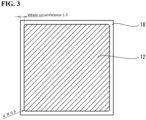
- FIG. 3 is a schematic view for explaining the shape of a heat sink pattern formed on the other surface of the bonded substrate of an example.
- an average crystal grain size and dislocation density in the copper sheet, a peel (bonding) strength between the copper sheet and the ceramic substrate, a flexural strength of the circuit board, and a furnace pass durability were measured and evaluated.
- the peel strength and flexural strength are indicators related to a damage accumulated in the ceramic substrate during the manufacturing step of the bonded substrate (abundance ratio of microcracks in ceramics), and the higher these strengths are, the less damage accumulates in the ceramic substrate of a finally obtained bonded substrate, and the higher the heat cycle resistance of the bonded substrate is.
- the furnace pass durability is an acceleration test of heat treatment (heat cycle properties) that evaluates the effect of heating when assembling a power module using a circuit board, simulating the case where the circuit board is passed through a furnace during assembly.
- heat cycle properties heat cycle properties
- the crystal grain size of the copper sheet was evaluated by an intercept method described in JIS H 0501. Specifically, the evaluation is as follows. First, a copper sheet surface of the bonded substrate was corroded with an etching solution for observing a copper structure to make the crystal grains easier to see, and then an optical microscope image (magnification 100x, field of view size 3.5 mm x 2.6 mm) was taken. A line segment (length 3.5 mm) for evaluation of the intercept method was drawn in the center of the obtained image, and the number of crystals cut by the line segment was counted and divided by the cutting length of 3.5 mm, to thereby calculate a particle size in that field. This operation was performed for arbitrary five visual fields, and an average value was taken as an average crystal grain size of the bonded substrate.
- the dislocation density of the copper sheet was measured by X-ray diffraction line profile method (mWH/WA method) for the circuit board (stack) obtained by dividing and before applying electroless Ni-P plating. Specifically, first, in order to remove any surface defects that may have occurred during handling, the divided stacks were subjected to chemical polishing by immersing them for 5 minutes in a chemical polishing solution (45°C) consisting of 14% by mass of sulfuric acid, 3.2% by mass of hydrogen peroxide, with a remainder being water. Thereby, the surface defect layer formed on the surface of the copper sheet was removed. Then, the dislocation density of the copper sheet was measured for the chemically polished stack by the X-ray diffraction line profile method (mWH/WA method), with a central portion of the copper sheet surface of the heat sink pattern as a measurement point.
- mWH/WA method X-ray diffraction line profile method
- the dislocation density was measured using an X-ray diffraction measurement device ("SmartLab” manufactured by Rigaku Corporation).
- An X-ray source was a Cu tube (tube voltage 45 kV, tube current 200 mA), and X-ray was monochromatized to CuK ⁇ rays by an incident-side multilayer mirror.
- An optical system (arrangement of the X-ray source and detector) was based on a symmetric reflection method (focusing method).
- the peel strength of the circuit board was measured by a 90° peeling method (based on JIS C 5016, crosshead speed 50 mm/min) using a portion of the circuit pattern with a pattern width of 3 mm (a top pattern in FIG. 2 ). In this example, five pieces of circuit boards were evaluated, and an average value of the measurements at five points was taken as a peel strength.
- a flexural strength was measured by a three-point bending strength measurement (based on JIS C2141, distance between lower supports 30 mm, with a circuit pattern surface placed downward and load applied from above). In this example, five pieces of circuit boards were evaluated, and an average value was taken as a flexural strength.
- a furnace pass durability was evaluated using a batch furnace equipped with an internal carbon hot plate and a water-cooled cooling plate on the underside facing the hot plate that can be raised and lowered to switch between contact and noncontact.
- the circuit board was placed on a top surface of the hot plate of the batch furnace, and was subjected to a heat load by repeatedly passing through the furnace.
- the temperature profile for one heat load in the furnace is as follows: the hot plate was heated to a maximum temperature of 380°C at an average heating rate of approximately 1.0°C/s, with the cooling plate not in contact with the hot plate, and then held at a maximum temperature of 380°C for 10 minutes.
- the cooling plate was then brought into contact with the hot plate to rapidly cool to room temperature (an average cooling rate from 380°C to 100°C is approximately 2.5°C/s, and an average cooling rate from 100°C to 40°C is approximately 0.5°C/s). This process was counted as one cycle.
- the circuit board is repeatedly subjected to a furnace heat load, and the ceramic substrate of the circuit board is inspected with a microscope every three furnace heat loads, and the number of times when a crack was first found on the ceramic substrate was recorded as a furnace pass durability value of that piece.
- This furnace pass durability test was performed to 10 pieces of circuit boards, and a Weibull plot analysis was performed to the furnace pass durability test results to estimate the Weibull distribution of the furnace pass durability. An expected value of the Weibull distribution was calculated from the estimated Weibull distribution, and the result was obtained as an expected furnace pass durability value.
- the circuit board Since the circuit board has an electroless Ni-P plating film, it is more likely to induce cracks in the ceramic substrate due to heat load than a state without plating, and the evaluation can be completed with fewer furnace heat load cycles compared to a state without plating.
- samples 1 to 5 copper sheets A to E containing P, S, As, Sb and Zn within a predetermined range were used, and it was confirmed that the dislocation density in the copper sheets could be adjusted to 1.5 ⁇ 10 13 m -2 or less when bonding with a ceramic substrate to create a bonded substrate. Further, the circuit boards produced from the bonded substrates of samples 1 to 5 had peel strengths of 300 N/cm or more and flexural strengths of 400 MPa or more. Therefore, it was confirmed that damage to the ceramic substrate (the occurrence of microcracks) caused by the heat load during the circuit board production process can be suppressed.
- sample 6 since copper sheet F containing more than the prescribed amounts of S, As, Sb, and Zn was used, it was confirmed that the dislocation density in the copper sheet of the bonded substrate was as large as 2.2 ⁇ 10 13 m -2 . This is presumably because there are many S, As, Sb, and Zn, which increase the recrystallization temperature, and little P, which suppresses the increase in recrystallization temperature due to S, so Cu cannot be efficiently recrystallized during bonding and dislocations cannot be reduced. Further, it was confirmed that Sample 6 had smaller peel strength and flexural strength than Samples 1 to 5.
- the copper sheet became work-hardened during the production process of the circuit board, which increased the heat stress applied to the ceramic substrate, causing damage to the ceramic substrate. It was also confirmed that the ceramic substrate had a low furnace pass durability and was easily damaged by repeated heat loads being applied to the circuit board.
- the dislocation density in the copper sheet can be reduced by heating when bonding to the ceramic substrate, and high heat cycle performance can be achieved.
Landscapes
- Engineering & Computer Science (AREA)
- Chemical & Material Sciences (AREA)
- Ceramic Engineering (AREA)
- Materials Engineering (AREA)
- Organic Chemistry (AREA)
- Structural Engineering (AREA)
- Mechanical Engineering (AREA)
- Manufacturing & Machinery (AREA)
- Metallurgy (AREA)
- Microelectronics & Electronic Packaging (AREA)
- Inorganic Chemistry (AREA)
- Physics & Mathematics (AREA)
- Fluid Mechanics (AREA)
- Ceramic Products (AREA)
Applications Claiming Priority (2)
| Application Number | Priority Date | Filing Date | Title |
|---|---|---|---|
| JP2022039743A JP2023134291A (ja) | 2022-03-14 | 2022-03-14 | 銅-セラミックス接合基板およびその製造方法 |
| PCT/JP2022/043042 WO2023176045A1 (ja) | 2022-03-14 | 2022-11-21 | 銅-セラミックス接合基板およびその製造方法 |
Publications (1)
| Publication Number | Publication Date |
|---|---|
| EP4495280A1 true EP4495280A1 (de) | 2025-01-22 |
Family
ID=88023229
Family Applications (1)
| Application Number | Title | Priority Date | Filing Date |
|---|---|---|---|
| EP22932308.4A Pending EP4495280A1 (de) | 2022-03-14 | 2022-11-21 | Kupfer-/keramikgebundenes substrat und herstellungsverfahren dafür |
Country Status (6)
| Country | Link |
|---|---|
| US (1) | US20250171369A1 (de) |
| EP (1) | EP4495280A1 (de) |
| JP (1) | JP2023134291A (de) |
| KR (1) | KR20240116765A (de) |
| CN (1) | CN118742527A (de) |
| WO (1) | WO2023176045A1 (de) |
Family Cites Families (12)
| Publication number | Priority date | Publication date | Assignee | Title |
|---|---|---|---|---|
| JPS63231802A (ja) * | 1987-03-19 | 1988-09-27 | 古河電気工業株式会社 | 信号伝送用導体 |
| JPH0897554A (ja) | 1994-09-22 | 1996-04-12 | Dowa Mining Co Ltd | セラミックス配線基板の製造法 |
| JP3512977B2 (ja) | 1996-08-27 | 2004-03-31 | 同和鉱業株式会社 | 高信頼性半導体用基板 |
| JP2012114203A (ja) | 2010-11-24 | 2012-06-14 | Mitsubishi Electric Corp | 絶縁基板とその製造方法および電力半導体装置 |
| JP2012136378A (ja) * | 2010-12-25 | 2012-07-19 | Kyocera Corp | 回路基板およびこれを用いた電子装置 |
| KR20140025607A (ko) * | 2011-08-04 | 2014-03-04 | 가부시키가이샤 고베 세이코쇼 | 구리 합금 |
| WO2014196563A1 (ja) * | 2013-06-04 | 2014-12-11 | 日本碍子株式会社 | 銅合金の製造方法および銅合金 |
| JP7380550B2 (ja) * | 2018-12-13 | 2023-11-15 | 三菱マテリアル株式会社 | 純銅板 |
| TWI870562B (zh) * | 2020-03-06 | 2025-01-21 | 日商三菱綜合材料股份有限公司 | 純銅板 |
| JP7537900B2 (ja) * | 2020-03-31 | 2024-08-21 | Dowaメタルテック株式会社 | ろう材およびその製造方法並びに金属-セラミックス接合基板の製造方法 |
| JP7078070B2 (ja) * | 2020-06-30 | 2022-05-31 | 三菱マテリアル株式会社 | 銅合金、銅合金塑性加工材、電子・電気機器用部品、端子、バスバー、リードフレーム |
| EP4174199B1 (de) * | 2020-06-30 | 2025-12-03 | Mitsubishi Materials Corporation | Kupferlegierung, kupferlegierungskunststoffarbeitsmaterial, komponente für elektronische/elektrische vorrichtungen, klemme, sammelschiene, leiterrahmen und wärmeableitsubstrat |
-
2022
- 2022-03-14 JP JP2022039743A patent/JP2023134291A/ja active Pending
- 2022-11-21 KR KR1020247021264A patent/KR20240116765A/ko active Pending
- 2022-11-21 CN CN202280092342.3A patent/CN118742527A/zh active Pending
- 2022-11-21 WO PCT/JP2022/043042 patent/WO2023176045A1/ja not_active Ceased
- 2022-11-21 US US18/842,569 patent/US20250171369A1/en active Pending
- 2022-11-21 EP EP22932308.4A patent/EP4495280A1/de active Pending
Also Published As
| Publication number | Publication date |
|---|---|
| WO2023176045A1 (ja) | 2023-09-21 |
| JP2023134291A (ja) | 2023-09-27 |
| KR20240116765A (ko) | 2024-07-30 |
| CN118742527A (zh) | 2024-10-01 |
| US20250171369A1 (en) | 2025-05-29 |
Similar Documents
| Publication | Publication Date | Title |
|---|---|---|
| EP3632879B1 (de) | Keramische leiterplatte und sein herstellungsverfahren | |
| EP3471517B1 (de) | Keramisches schaltungssubstrat und verfahren zur herstellung eines keramischen schaltungssubstrats | |
| EP2911192B1 (de) | Substrat für ein strommodul mit einem kühlkörper, strommodul mit einem kühlkörper und verfahren zur herstellung des substrats für das strommodul mit einem kühlkörper | |
| CN113632217B (zh) | 氮化硅基板、氮化硅-金属复合体、氮化硅电路基板及半导体封装件 | |
| EP0999589B2 (de) | Schaltungssubstrat aus Siliziumnitrid | |
| EP2492958B1 (de) | Substrat für ein strommodul, substrat mit kühlkörper für ein strommodul, strommodul, verfahren zur herstellung des substrats für ein strommodul sowie verfahren zur herstellung des substrats mit kühlkörper für ein strommodul | |
| EP2833400B1 (de) | Leistungsmodulsubstrat mit kühlkörper und verfahren zur herstellung des leistungsmodulsubstrats mit dem kühlkörper | |
| EP1420445B1 (de) | Wärmeableitplatte und leistungshalbleitermodul | |
| EP3632880B1 (de) | Keramikleiterplatte und verfahren zur herstellung davon | |
| JPH09157054A (ja) | 回路基板 | |
| EP0766307B1 (de) | Schaltungssubstrat aus siliziumnitrid | |
| EP4378913A1 (de) | Kupfer/keramik verbundkörper und isolierte leiterplatte | |
| EP4495280A1 (de) | Kupfer-/keramikgebundenes substrat und herstellungsverfahren dafür | |
| EP1142849B1 (de) | Substrat auf der basis eines siliziumnitridkomposits | |
| JP2007059178A (ja) | ヒータユニットおよびそれを備えた装置 | |
| US20250087576A1 (en) | Bonded body, ceramic circuit board, semiconductor device, and method for manufacturing bonded body | |
| EP4495087A1 (de) | Kupfer-/keramikgebundenes substrat und herstellungsverfahren dafür | |
| EP4585581A1 (de) | Kupfer/keramik verbundkörper und isolierte leiterplatte | |
| EP4503115A1 (de) | Keramisches schaltungssubstrat und halbleiteranordnung damit | |
| EP2933831A1 (de) | Verfahren zur herstellung eines substrats für leistungsmodule | |
| EP3961694B1 (de) | Elektronisches komponentenmodul und schaltsubstrat aus siliziumnitrid | |
| EP3951854A1 (de) | Leiterplatte aus siliziumnitrid und elektronisches komponentenmodul | |
| EP4378914A1 (de) | Kupfer/keramik verbundkörper und isolierte leiterplatte | |
| US20230260868A1 (en) | Bonded body, ceramic-copper circuit board, and semiconductor device | |
| EP4328208A1 (de) | Kupfer/keramik verbundkörper und isolierte leiterplatte |
Legal Events
| Date | Code | Title | Description |
|---|---|---|---|
| STAA | Information on the status of an ep patent application or granted ep patent |
Free format text: STATUS: THE INTERNATIONAL PUBLICATION HAS BEEN MADE |
|
| PUAI | Public reference made under article 153(3) epc to a published international application that has entered the european phase |
Free format text: ORIGINAL CODE: 0009012 |
|
| STAA | Information on the status of an ep patent application or granted ep patent |
Free format text: STATUS: REQUEST FOR EXAMINATION WAS MADE |
|
| 17P | Request for examination filed |
Effective date: 20240926 |
|
| AK | Designated contracting states |
Kind code of ref document: A1 Designated state(s): AL AT BE BG CH CY CZ DE DK EE ES FI FR GB GR HR HU IE IS IT LI LT LU LV MC ME MK MT NL NO PL PT RO RS SE SI SK SM TR |
|
| DAV | Request for validation of the european patent (deleted) | ||
| DAX | Request for extension of the european patent (deleted) |