EP4503336A1 - Élément de contact pour la mise en contact électrique d'au moins deux éléments de contact électriques, agencement et procédé de mise en contact d'éléments de contact électriques au moyen d'un soudage laser - Google Patents
Élément de contact pour la mise en contact électrique d'au moins deux éléments de contact électriques, agencement et procédé de mise en contact d'éléments de contact électriques au moyen d'un soudage laser Download PDFInfo
- Publication number
- EP4503336A1 EP4503336A1 EP23189779.4A EP23189779A EP4503336A1 EP 4503336 A1 EP4503336 A1 EP 4503336A1 EP 23189779 A EP23189779 A EP 23189779A EP 4503336 A1 EP4503336 A1 EP 4503336A1
- Authority
- EP
- European Patent Office
- Prior art keywords
- contacting
- support
- contact element
- electrical contact
- support region
- Prior art date
- Legal status (The legal status is an assumption and is not a legal conclusion. Google has not performed a legal analysis and makes no representation as to the accuracy of the status listed.)
- Withdrawn
Links
Images


Classifications
-
- H—ELECTRICITY
- H01—ELECTRIC ELEMENTS
- H01R—ELECTRICALLY-CONDUCTIVE CONNECTIONS; STRUCTURAL ASSOCIATIONS OF A PLURALITY OF MUTUALLY-INSULATED ELECTRICAL CONNECTING ELEMENTS; COUPLING DEVICES; CURRENT COLLECTORS
- H01R4/00—Electrically-conductive connections between two or more conductive members in direct contact, i.e. touching one another; Means for effecting or maintaining such contact; Electrically-conductive connections having two or more spaced connecting locations for conductors and using contact members penetrating insulation
- H01R4/02—Soldered or welded connections
- H01R4/029—Welded connections
-
- B—PERFORMING OPERATIONS; TRANSPORTING
- B23—MACHINE TOOLS; METAL-WORKING NOT OTHERWISE PROVIDED FOR
- B23K—SOLDERING OR UNSOLDERING; WELDING; CLADDING OR PLATING BY SOLDERING OR WELDING; CUTTING BY APPLYING HEAT LOCALLY, e.g. FLAME CUTTING; WORKING BY LASER BEAM
- B23K26/00—Working by laser beam, e.g. welding, cutting or boring
- B23K26/20—Bonding
- B23K26/21—Bonding by welding
- B23K26/22—Spot welding
-
- B—PERFORMING OPERATIONS; TRANSPORTING
- B23—MACHINE TOOLS; METAL-WORKING NOT OTHERWISE PROVIDED FOR
- B23K—SOLDERING OR UNSOLDERING; WELDING; CLADDING OR PLATING BY SOLDERING OR WELDING; CUTTING BY APPLYING HEAT LOCALLY, e.g. FLAME CUTTING; WORKING BY LASER BEAM
- B23K26/00—Working by laser beam, e.g. welding, cutting or boring
- B23K26/20—Bonding
- B23K26/21—Bonding by welding
- B23K26/24—Seam welding
- B23K26/244—Overlap seam welding
-
- H—ELECTRICITY
- H01—ELECTRIC ELEMENTS
- H01R—ELECTRICALLY-CONDUCTIVE CONNECTIONS; STRUCTURAL ASSOCIATIONS OF A PLURALITY OF MUTUALLY-INSULATED ELECTRICAL CONNECTING ELEMENTS; COUPLING DEVICES; CURRENT COLLECTORS
- H01R43/00—Apparatus or processes specially adapted for manufacturing, assembling, maintaining, or repairing of line connectors or current collectors or for joining electric conductors
- H01R43/02—Apparatus or processes specially adapted for manufacturing, assembling, maintaining, or repairing of line connectors or current collectors or for joining electric conductors for soldered or welded connections
- H01R43/0221—Laser welding
-
- B—PERFORMING OPERATIONS; TRANSPORTING
- B23—MACHINE TOOLS; METAL-WORKING NOT OTHERWISE PROVIDED FOR
- B23K—SOLDERING OR UNSOLDERING; WELDING; CLADDING OR PLATING BY SOLDERING OR WELDING; CUTTING BY APPLYING HEAT LOCALLY, e.g. FLAME CUTTING; WORKING BY LASER BEAM
- B23K2101/00—Articles made by soldering, welding or cutting
- B23K2101/36—Electric or electronic devices
- B23K2101/38—Conductors
-
- B—PERFORMING OPERATIONS; TRANSPORTING
- B23—MACHINE TOOLS; METAL-WORKING NOT OTHERWISE PROVIDED FOR
- B23K—SOLDERING OR UNSOLDERING; WELDING; CLADDING OR PLATING BY SOLDERING OR WELDING; CUTTING BY APPLYING HEAT LOCALLY, e.g. FLAME CUTTING; WORKING BY LASER BEAM
- B23K2103/00—Materials to be soldered, welded or cut
- B23K2103/08—Non-ferrous metals or alloys
- B23K2103/12—Copper or alloys thereof
Definitions
- the invention relates to a contacting element for electrically contacting at least two electrical contact elements. Furthermore, the invention relates to an arrangement with a first and a second electrical contact element, wherein the two electrical contact elements are contacted by means of a corresponding contacting element. The invention also relates to a method for contacting at least two electrical contact elements by means of a laser beam welding method.
- the coupling of the laser beam into the material must first be ensured.
- the wavelength of the laser radiation must be adapted to the material in order to achieve the highest possible light absorption.
- the coupling can be improved at a wavelength of 1.06 um by applying a thin, less reflective layer or by changing the surface, for example by tinning or nickel plating.
- This increases the effort and is also technically demanding.
- the roughness of the surface or oxide layers also influence the reflection-absorption behavior of the material.
- the reflectivity decreases with increasing temperature. As soon as the copper surface melts, a multiple of the laser power is absorbed compared to a bare copper surface at room temperature. If a sufficiently high laser power or laser power density is used, the material is first heated, which is accompanied by absorption. With increased coupling of the laser beam, a vapor capillary is formed in the melt, a so-called keyhole. This is followed by multiple reflections on the keyhole wall, i.e. the laser beam is completely absorbed. As soon as a keyhole has formed, the entire laser power is suddenly coupled into the workpiece.
- An object of the present invention is to improve contacting of electrical contacts by means of a laser beam welding process.
- the contacting element according to the invention can advantageously be used for contacting electrical contacts by means of laser beam welding or a laser beam welding process. At least two different electrical contact elements or electrical contacts arranged or positioned at a distance from one another can be electrically contacted, coupled or contacted by means of the contacting element.
- the contacting element can be designed as a contact bridge, contact plate, busbar or another connecting element for current transmission.
- the contacting element can be used in a production process or in the manufacture of power electronics parts and/or electronic components.
- the two electrical contact elements or electrical contacts can be contacts of electronic components or electrical components such as semiconductors, coils or capacitors.
- the electrical contact elements can be located within a printed circuit board or an integrated circuit or any other electronic component.
- the two electrical contacts or electrical contact elements can each be a positive pole or a negative pole, so that an electrical connection can be established between the two contact elements by means of the contacting element.
- the contacting element Since such electronic components are very sensitive, a low energy input is advantageous when making contact using laser beam welding in order to avoid causing damage.
- the respective substance or material should melt slightly. This is achieved in particular by the contacting element resting on the electrical contact elements and in particular on their surface by means of the support areas, in particular at specific points. In other words, the contacting element rests on the contact elements exclusively by means of the support areas.
- a laser beam or laser radiation from a laser beam welding process is introduced or acted on in particular these support areas.
- these predetermined or specially designed support areas provide a precise, in particular exact support of the elements to be fused or connected.
- the contacting element lies directly on the contact elements using the support areas, so that in particular the support areas lie directly on the surface or on the surface of the contact elements or contacts. This means that a point-based and precise contact can be made without melting too large a volume of material and reducing or setting a zero gap between two elements or components to be contacted.
- the support areas are designed in such a way that they protrude towards the respective surface of the contact elements or protrude outwards.
- the contacting element thus rests on these point-based or predetermined support areas.
- the contacting element can be designed as a copper plate or as another metallic, electrically conductive plate or sheet or wire.
- the contacting element according to the invention zero gaps can be easily achieved for laser contacting of sensitive components.
- low volume melting can be achieved when using laser beam welding, so that less thermomechanical stress occurs in electronic components.
- an upper contact partner (“lead frame”) can be produced simply and inexpensively.
- the first support area and the second support area are spherical, wherein the first support area during a contacting process to the first electrical contact element and the second support area during the contacting process to the second electrical contact element. Due to this curved or bulbous or spherical design of the support areas, the contacting element rests on these spherical designs of the support areas. In other words, a point-based support can be provided so that the welding points can be set in these support areas. In other words, the first and/or the second support area or further support areas can be designed as a bulge, recess, cutout or notch.
- the support areas are designed in such a way that they are curved towards the surfaces of the contact elements, i.e. outwards, during contacting, i.e. when the contacting element is applied or placed or plugged onto the contact elements.
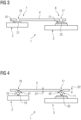
- first support area and the second support area are pyramid-shaped, with a tip of the pyramid-shaped first support area being directed towards the first electrical contact element during a contacting process and a tip of the pyramid-shaped second support area being directed towards the second electrical contact element during the contacting process.
- These pyramid-shaped, i.e. triangular, support areas can be used to create a point-like and thus direct support of the contacting element on the contact elements.
- the pyramid-shaped or triangular design of the support areas is designed such that during a contacting process and thus the attachment of the contacting element to or on the contact elements, the contacting element is connected to the contact elements, in particular exclusively, by means of the tips of the pyramid-shaped support areas. This creates a zero gap on the one hand and laser beam welding can then begin at the areas of the tips.
- the first support area and the second support area are designed in a plateau-shaped manner, with an outer side of the plateau-shaped first support area, which is parallel to the first contacting side, being directed towards the first electrical contact element during a contacting process, and an outer side of the plateau-shaped second support area, which is parallel to the second contacting side, being directed towards the second electrical contact element during a contacting process.
- the support areas are designed as an elevation or as a plateau, which is directed towards the surface of the contact elements when contact is made or when an electrical connection is established between the contact elements.
- the contacting element when the contacting element is in contact with the contact elements, the contacting element rests on the contact elements, in particular exclusively or only by means of the outer sides of the plateau-shaped support areas. This makes it possible to achieve a zero gap and only a small amount of material can be melted for the subsequent laser beam welding for the firm contact, namely the material in the area of the outer side of the support areas.
- the number of respective support areas can also depend on a type and/or type of contact element to be contacted. In this case, a dimension, in particular a size of the contact elements, is particularly crucial. The larger and in particular the larger the surface of the contact elements, the more support areas can be provided.
- the support areas are produced by means of a punching process, a pressing process, or a rolling process.
- an appropriate process can be selected.
- the contacting element can be manufactured together in one process. This means that, for example, the bending angle and the support areas can be manufactured or incorporated simultaneously in one processing step.
- a further aspect (second aspect) relates to an arrangement with a first and a second electrical contact element or electrical contact, wherein the two electrical contact elements are electrically contacted by means of a contacting element according to the previous aspect or an advantageous development thereof.
- the contacting element explained at the outset according to the first aspect can advantageously be used to electrically contact the electrical contact elements with one another.
- the contacting element can be used here as a busbar or contact bridge.
- several such contacting elements can be used to contact contact elements.
- the first contacting side of the contacting element is coupled to the first contact element by means of the first support region, which at least partially rests on the surface of the first contact element. Furthermore, the second contacting side of the contacting element is coupled to the second contact element by means of the second support region, which at least partially rests on the surface of the second contact element.
- This provides an electrical connection, in particular a fixed one, between the first and the second contact element. This can be achieved, for example, by means of a laser beam welding process.
- the contact element rests on or against the respective surface of a contact element according to the support regions or exclusively by means of the support regions.
- the arrangement provides, in particular, an electrical connection with essentially minimal losses and thus an electrical current transmission between the contact elements.
- the first support area is at least partially bonded to the first contact element by means of a laser beam welding process and the second support area is at least partially bonded to the second contact element by means of the laser beam welding process.
- the materials of the contacting element and the contact elements can be melted or fused on the support surfaces or support points, i.e. the support areas that lie on the surface of the contact elements.
- an electrical connection and thus a flow of current from the contact elements to one another is possible via a bonded connection with the contacting element.
- the contacting element is connected or coupled to the contact element via the support area. This means that current flows via the material connection between the contact element and the support area.
- the contacting element is contacted with the two contact elements at points or over a surface or evenly by means of the support areas.
- the arrangement has the advantage above all that the contact points between the contacting element, which can be a copper track, for example, and the contact element have no gap and thus a zero gap. This is achieved by making contact by fusing the material of the contact areas with the contact elements. This means that there is point contact, which cannot have a zero gap, since there is a material connection here, and that only a few points are melted using a laser beam welding process, namely the contact areas.
- the proposed method enables more efficient contacting of electrical contacts of electrical components.
- a laser beam welding method is advantageously used for this purpose. With the help of the laser beam welding method, an electrical connection between two components, in this case the contacting element with the contact elements, can be realized without contact using a laser beam.
- the process can be used in the manufacture of electronic components or power electronic components.
- positioning and melting can be carried out using an automated system or an automated device.
- a contacting system or a contacting device can be used as an automatic, electromechanical unit in order to be able to contact the electrical contact elements automatically.
- a laser unit is used to introduce energy into the area in which a respective support area rests on a respective surface of the contact elements in order to melt the material there.
- a material bond i.e. a melt bond
- a good electrical contact is ensured.
- an error message and/or a request to enter user feedback is issued and/or a default setting and/or a predetermined initial state is set.
- the invention also includes further developments of the arrangement according to the invention and of the method according to the invention, which have features as have already been described in connection with the further developments of the contacting element according to the invention. For this reason, the corresponding further developments of the arrangement according to the invention and of the method according to the invention are not described again here.
- the invention also includes combinations of the features of the described embodiments.
- the arrangement 1 comprises a first electrical contact element 2 (an electrical contact) and at least one further, in particular to the first contact element 2 different or separate, second electrical contact element 3.
- the contact elements 2, 3 are electrical contacts which can be referred to as current or voltage connections.
- FIG 1 an exemplary side view is shown.
- a contacting element 4 is provided according to the invention.
- This contacting element 4 can be an electrical connection for current transmission.
- the contacting element 4 can be a wire, a copper sheet, a metallic element or another electrically conductive element.
- the latter is specially designed, in particular pre-processed.
- the arrangement 1 can, for example, be part of an electronic component or a power electronic component.
- the contact element 3 can be multi-layered or multi-part, as in the FIG 1 shown as an example.
- the contact element 2 can in turn be formed in one piece.
- the contact element 3 can have a power supply 5 for an electronic component 6 located underneath, which is particularly sensitive.
- This component can in turn be arranged on a circuit board or an electrical device.
- the contacting element 4 is contacted with the contact elements 2, 3 by means of a selective or individual laser beam welding process.
- a selective or individual laser beam welding process For this purpose, at specially specified locations or Points or areas of the contacting element 4 can be subjected to an energy input for welding.
- the contacting element 4 has a first contacting side 7 and a second contacting side 8. Viewed in the x-direction, these can be the opposite end sides of the contacting element 4.
- the contact element 2 can be contacted or electrically connected or coupled by means of the first contacting side 7 and the second contacting element 3 can be contacted or electrically connected or coupled by means of the second contacting side 8.
- the contacting element 4 has at least two support areas 10, 11.
- the first support area 10 is part of the first contact side 7 and the second support area 11 is part of the second contact side 8.
- These support areas 10, 11 can be specially designed or formed sub-areas of the contact sides 7, 8.
- the support areas 10, 11 can be used to provide a point-by-point support of the contacting element 4 in relation to the contact elements 2, 3. This offers the advantage that, on the one hand, the support areas 10, 11, i.e. on support points or support surfaces, are in direct contact with the contact elements 2, 3 and thus there is no gap or only a small gap.
- support areas 10, 11 can be by means of a laser unit 12, melting of the material there can be realized or carried out.
- the first support area 10 rests on a surface 13 of the contact element 2 at least in some areas, in particular directly.
- the second support area 11 rests on or on a surface 14 of the second contact element 3, in particular directly.
- melting can be caused by means of a laser beam, for example, in order to realize a material-locking connection here.
- the support areas 10, 11 protrude outwards (in the negative z-direction) in relation to a respective main extension plane of the contacting sides 7, 8 or towards the contact element 2, 3. This provides a point-based support for the contacting element 4.
- the support areas 10, 11 can be referred to as tapering of a material thickness of the contacting element 4. This can reduce the melting volume, since melting takes place within these taperings using the laser unit 12.
- the taperings proposed for this purpose, i.e. the areas 10, 11, can be point-shaped or linear supports.
- the first contacting side can have a material thickness D1 and the second contacting side 8 a material thickness D2.
- the two material thicknesses D1, D2 can be the same.
- a material thickness d1 of the first support area 10 can be smaller than the material thickness D1.
- a material thickness d2 of the second support area 11 can in turn be smaller than the material thickness D2, or support surfaces 10, 11 can be produced using punching processes, pressing processes or rolling processes.
- the material thickness d1, d2 can have a material thickness of approximately 5 ⁇ m to 500 ⁇ m. This would be the case if sensitive Components are to be connected or welded, as a smaller melting volume should be used here.
- the thicknesses d1, d2 can also be greater than 500 ⁇ m.
- the contacting element 4 can, for example, be referred to as a molded part. This can have an increased bending tolerance and yet still have at least a zero gap 9.
- the contact elements 2, 3 are at different heights from one another.
- the contact elements 2, 3 have a height difference h in the z direction.
- the contacting element 4 can be adapted to suit the specific user or situation.
- the contacting element 4 can be bent, as shown here.
- the height difference h can be compensated for accordingly by taking a bending angle 15 into account.
- the bending angle 15 is essentially 90 degrees, so that there is a right-angled bend.
- the contacting sides 7, 8 are parallel and spaced apart from one another.
- the contact sides 7, 8 can have several support areas. This offers advantages when melting or when creating the material connection, since better electrical contact can be achieved and the required heat input and the required melting volume at specific points can be kept low. If several support areas or tapers are located next to one another, contact between all support areas and the respective contact element 2, 3 can be achieved with a much simpler bending device ("bending tool"), since the tapers can be easily deformed. The result can be a good connection to the workpiece or contacting element 4.
- the tapering of the material thickness can reduce the volume of metal to be melted, such as a volume of copper.
- a mutually flat or essentially flat arrangement or positioning of the contact elements 2, 3 can also be provided. This is, for example, in the FIG 2 shown.
- the support areas 10, 11 can be designed in a variety of ways.
- the support areas 10, 11 can be referred to as material tapers.
- any geometric design can be made here.
- other geometries are also conceivable, such as a double sphere, a triple sphere, a quadruple sphere or a pyramid geometry. The reason for this is that the tapering of the material thickness can then partially deform better upon contact and thus it can be ensured that a zero gap 9 is present.
- the laser unit 12 can be controlled accordingly so that the laser can couple into the corresponding position of the support areas 10, 11.
- the support areas 10, 11 have a spherical shape or a spherical geometry. In this case, they are shown in particular as hemispheres, in particular as hollow hemispheres.
- the first support area 10, 11 can be pyramid-shaped or triangular, as is the case, for example, in the FIG 4 can be seen.
- the areas 16, 17 are filled with air and do not have any material of the contacting element 4.
- a respective tip of these pyramid-shaped geometries (cf. FIG 4 ) is arranged in the direction of the contact elements 2, 3.
- the tips 19, 20 of the pyramid-shaped support areas 10, 11 point in the negative z-direction towards the contact elements 2, 3 to be contacted.
- the spherical support areas 10, 11 are curved in such a way that they are curved in the negative z-direction towards the contact elements 2, 3.
- the support areas 10, 11 can be designed as a support area directed towards the contact elements 2, 3.
- a respective outer side 21, 22 of the support areas 10, 11 can each lie parallel to the surfaces 13, 14 of the contact elements 2, 3.
- the contacting elements 4 can have a knob-like shape when viewed in the positive z-direction, i.e. viewed from below, since the support areas 10, 11 can represent knobs when viewed from this underside. These knobs in turn rest on or against the contact elements 2, 3.
- the contacting element 4 can be produced in one or more processing steps.
- a sheet metal can be cut or bent accordingly.
- the support areas 10, 11 can be incorporated into the material or into the sheet-like contacting element 4 by means of punching, rolling or pressing.
- the contacting element 4 can be placed or placed on the contact elements 2, 3, in particular from above.
- the contacting element 4 rests on the contact elements 2, 3 by means of the support areas 10, 11.
- the contacting element 4 can be adjusted accordingly depending on the application and in particular depending on the contacting process, so that, for example, the height difference h can be compensated.
- the contacting element 4 can be bent.
- the material can be melted in the area of the support areas 10, 11
- the laser unit 12 can provide a corresponding energy input by means of a laser beam.
- a material-locking connection can be realized or produced, so that the two contact elements 2, 3 are electrically connected via material-locking connections between the contacting element 4 and the contact elements 2, 3.
- the described embodiments can be used to perform geometry optimization for laser welding of thermal and electrically conductive connections.
Landscapes
- Physics & Mathematics (AREA)
- Optics & Photonics (AREA)
- Engineering & Computer Science (AREA)
- Plasma & Fusion (AREA)
- Mechanical Engineering (AREA)
- Manufacturing & Machinery (AREA)
- Manufacture Of Switches (AREA)
- Connections Effected By Soldering, Adhesion, Or Permanent Deformation (AREA)
Priority Applications (4)
| Application Number | Priority Date | Filing Date | Title |
|---|---|---|---|
| EP23189779.4A EP4503336A1 (fr) | 2023-08-04 | 2023-08-04 | Élément de contact pour la mise en contact électrique d'au moins deux éléments de contact électriques, agencement et procédé de mise en contact d'éléments de contact électriques au moyen d'un soudage laser |
| EP24754581.7A EP4736270A1 (fr) | 2023-08-04 | 2024-07-30 | Élément de contact pour la mise en contact électrique d'au moins deux éléments de contact électrique, agencement et procédé de mise en contact d'éléments de contact électrique au moyen d'un soudage par faisceau laser |
| PCT/EP2024/071515 WO2025031874A1 (fr) | 2023-08-04 | 2024-07-30 | Élément de contact pour la mise en contact électrique d'au moins deux éléments de contact électrique, agencement et procédé de mise en contact d'éléments de contact électrique au moyen d'un soudage par faisceau laser |
| CN202480062870.3A CN121942098A (zh) | 2023-08-04 | 2024-07-30 | 用于电接触至少两个电接触元件的接触件、装置以及用于借助于激光束焊接来接触电接触元件的方法 |
Applications Claiming Priority (1)
| Application Number | Priority Date | Filing Date | Title |
|---|---|---|---|
| EP23189779.4A EP4503336A1 (fr) | 2023-08-04 | 2023-08-04 | Élément de contact pour la mise en contact électrique d'au moins deux éléments de contact électriques, agencement et procédé de mise en contact d'éléments de contact électriques au moyen d'un soudage laser |
Publications (1)
| Publication Number | Publication Date |
|---|---|
| EP4503336A1 true EP4503336A1 (fr) | 2025-02-05 |
Family
ID=87557770
Family Applications (2)
| Application Number | Title | Priority Date | Filing Date |
|---|---|---|---|
| EP23189779.4A Withdrawn EP4503336A1 (fr) | 2023-08-04 | 2023-08-04 | Élément de contact pour la mise en contact électrique d'au moins deux éléments de contact électriques, agencement et procédé de mise en contact d'éléments de contact électriques au moyen d'un soudage laser |
| EP24754581.7A Pending EP4736270A1 (fr) | 2023-08-04 | 2024-07-30 | Élément de contact pour la mise en contact électrique d'au moins deux éléments de contact électrique, agencement et procédé de mise en contact d'éléments de contact électrique au moyen d'un soudage par faisceau laser |
Family Applications After (1)
| Application Number | Title | Priority Date | Filing Date |
|---|---|---|---|
| EP24754581.7A Pending EP4736270A1 (fr) | 2023-08-04 | 2024-07-30 | Élément de contact pour la mise en contact électrique d'au moins deux éléments de contact électrique, agencement et procédé de mise en contact d'éléments de contact électrique au moyen d'un soudage par faisceau laser |
Country Status (3)
| Country | Link |
|---|---|
| EP (2) | EP4503336A1 (fr) |
| CN (1) | CN121942098A (fr) |
| WO (1) | WO2025031874A1 (fr) |
Citations (4)
| Publication number | Priority date | Publication date | Assignee | Title |
|---|---|---|---|---|
| WO2008062951A1 (fr) * | 2006-11-20 | 2008-05-29 | Lg Chem, Ltd. | Procédé pour la connexion d'un élément conducteur à un dispositif |
| DE202016008092U1 (de) * | 2016-12-28 | 2017-03-03 | Few Fahrzeugelektrikwerk Gmbh & Co. Kg | Elektrisches Anschlusselement |
| DE102021207276A1 (de) * | 2021-07-09 | 2023-01-12 | Robert Bosch Gesellschaft mit beschränkter Haftung | Verbindungsanordnung, insbesondere zur Verwendung in Elektrofahrzeugen oder Hybridfahrzeugen |
| EP4131661A1 (fr) * | 2020-04-01 | 2023-02-08 | Jilin Zhong Ying High Technology Co., Ltd. | Nouvelle borne de raccordement de fil conducteur et joint de soudure |
Family Cites Families (3)
| Publication number | Priority date | Publication date | Assignee | Title |
|---|---|---|---|---|
| JP6631866B2 (ja) * | 2015-01-09 | 2020-01-15 | 株式会社Gsユアサ | 蓄電装置 |
| JP6635294B2 (ja) * | 2015-12-15 | 2020-01-22 | 株式会社オートネットワーク技術研究所 | バスバー及び蓄電モジュール |
| DE102019001893A1 (de) * | 2019-03-18 | 2019-11-14 | Daimler Ag | Verfahren zur Herstellung von elektrischen Verbindungen wenigstens zweier Batteriezellen für eine Batterie eines Kraftfahrzeugs, insbesondere eines Kraftwagens |
-
2023
- 2023-08-04 EP EP23189779.4A patent/EP4503336A1/fr not_active Withdrawn
-
2024
- 2024-07-30 EP EP24754581.7A patent/EP4736270A1/fr active Pending
- 2024-07-30 CN CN202480062870.3A patent/CN121942098A/zh active Pending
- 2024-07-30 WO PCT/EP2024/071515 patent/WO2025031874A1/fr active Pending
Patent Citations (4)
| Publication number | Priority date | Publication date | Assignee | Title |
|---|---|---|---|---|
| WO2008062951A1 (fr) * | 2006-11-20 | 2008-05-29 | Lg Chem, Ltd. | Procédé pour la connexion d'un élément conducteur à un dispositif |
| DE202016008092U1 (de) * | 2016-12-28 | 2017-03-03 | Few Fahrzeugelektrikwerk Gmbh & Co. Kg | Elektrisches Anschlusselement |
| EP4131661A1 (fr) * | 2020-04-01 | 2023-02-08 | Jilin Zhong Ying High Technology Co., Ltd. | Nouvelle borne de raccordement de fil conducteur et joint de soudure |
| DE102021207276A1 (de) * | 2021-07-09 | 2023-01-12 | Robert Bosch Gesellschaft mit beschränkter Haftung | Verbindungsanordnung, insbesondere zur Verwendung in Elektrofahrzeugen oder Hybridfahrzeugen |
Also Published As
| Publication number | Publication date |
|---|---|
| CN121942098A (zh) | 2026-04-28 |
| EP4736270A1 (fr) | 2026-05-06 |
| WO2025031874A1 (fr) | 2025-02-13 |
Similar Documents
| Publication | Publication Date | Title |
|---|---|---|
| DE10066446B4 (de) | Verfahren zur Herstellung eines elektronischen Bauteils mit zwei Abstrahlungsbauteilen | |
| DE19653499B4 (de) | Lotzuführgerät und Lotzuführverfahren | |
| DE69026188T2 (de) | Elektrischer Verbinder | |
| DE3423172C2 (de) | Verfahren zum Herstellen einer Solarbatterie | |
| DE69523409T2 (de) | Herstellung von Lötverbindungen zur Verwendung in der Verpackung von elektrischen Schaltungen | |
| EP3103138B1 (fr) | Procédé de montage d'un composant électrique en utilisant un capot | |
| DE2442159A1 (de) | Verfahren zum verbinden von flachseiten miteinander und durch das verfahren hergestellte bauteile | |
| DE102018203715B4 (de) | Verfahren zur Herstellung einer Leiterplatte unter Verwendung einer Form für Leiterelemente | |
| WO2019219536A1 (fr) | Système de contact, module électronique comportant le système de contact et procédé de création du système de contact | |
| DE19522338B4 (de) | Chipträgeranordnung mit einer Durchkontaktierung | |
| WO2020007583A1 (fr) | Procédé de fabrication d'un joint brasé sans plomb résistant aux températures élevées, et joint brasé sans plomb résistant aux températures élevées | |
| EP2709786B1 (fr) | Procédé pour relier des éléments par liaison de matière | |
| WO2007033829A2 (fr) | Module semi-conducteur de puissance et son procede de production | |
| WO1997042798A1 (fr) | Procede de realisation de connexions electroconductrices entre au moins deux structures de conducteurs | |
| DE10212742A1 (de) | Verfahren zum Löten von Kontaktstiften und Kontaktstifte dazu | |
| EP1480291B1 (fr) | Assemblage électronique | |
| DE102009016842B4 (de) | Leitungsgitter für Elektronikgehäuse und Herstellungsverfahren | |
| EP4736270A1 (fr) | Élément de contact pour la mise en contact électrique d'au moins deux éléments de contact électrique, agencement et procédé de mise en contact d'éléments de contact électrique au moyen d'un soudage par faisceau laser | |
| DE10252577B4 (de) | Verfahren zum Erzeugen einer Lotverbindung durch kapillaren Lotfluß | |
| WO2024126042A1 (fr) | Connexion par contact d'une feuille conductrice flexible à une carte de circuit imprimé rigide et procédé d'établissement d'une telle connexion par contact | |
| DE10007414B4 (de) | Verfahren zur Durchkontaktierung eines Substrats für Leistungshalbleitermodule durch Lot und mit dem Verfahren hergestelltes Substrat | |
| WO1997008925A1 (fr) | Procede pour etablir une connexion entre au moins deux conducteurs electriques dont l'un est monte sur un substrat de support | |
| DE10341186A1 (de) | Verfahren und Vorrichtung zum Kontaktieren von Halbleiterchips | |
| DE102019106394B4 (de) | Verfahren zum Herstellen einer kohäsiven Verbindung und Bondmaterialvorform dafür | |
| EP3955713A1 (fr) | Carte de circuit imprimé permettant de raccorder une carte de circuit imprimé de contact agencée en parallèle |
Legal Events
| Date | Code | Title | Description |
|---|---|---|---|
| PUAI | Public reference made under article 153(3) epc to a published international application that has entered the european phase |
Free format text: ORIGINAL CODE: 0009012 |
|
| STAA | Information on the status of an ep patent application or granted ep patent |
Free format text: STATUS: THE APPLICATION HAS BEEN PUBLISHED |
|
| AK | Designated contracting states |
Kind code of ref document: A1 Designated state(s): AL AT BE BG CH CY CZ DE DK EE ES FI FR GB GR HR HU IE IS IT LI LT LU LV MC ME MK MT NL NO PL PT RO RS SE SI SK SM TR |
|
| STAA | Information on the status of an ep patent application or granted ep patent |
Free format text: STATUS: THE APPLICATION IS DEEMED TO BE WITHDRAWN |
|
| 18D | Application deemed to be withdrawn |
Effective date: 20250806 |