EP4510023A1 - Datenverarbeitungskomponente und computerprozessor - Google Patents
Datenverarbeitungskomponente und computerprozessor Download PDFInfo
- Publication number
- EP4510023A1 EP4510023A1 EP23192017.4A EP23192017A EP4510023A1 EP 4510023 A1 EP4510023 A1 EP 4510023A1 EP 23192017 A EP23192017 A EP 23192017A EP 4510023 A1 EP4510023 A1 EP 4510023A1
- Authority
- EP
- European Patent Office
- Prior art keywords
- data processing
- layer
- processing element
- output
- operational
- Prior art date
- Legal status (The legal status is an assumption and is not a legal conclusion. Google has not performed a legal analysis and makes no representation as to the accuracy of the status listed.)
- Pending
Links
Images

Classifications
-
- G—PHYSICS
- G06—COMPUTING OR CALCULATING; COUNTING
- G06F—ELECTRIC DIGITAL DATA PROCESSING
- G06F21/00—Security arrangements for protecting computers, components thereof, programs or data against unauthorised activity
- G06F21/70—Protecting specific internal or peripheral components, in which the protection of a component leads to protection of the entire computer
- G06F21/71—Protecting specific internal or peripheral components, in which the protection of a component leads to protection of the entire computer to assure secure computing or processing of information
- G06F21/75—Protecting specific internal or peripheral components, in which the protection of a component leads to protection of the entire computer to assure secure computing or processing of information by inhibiting the analysis of circuitry or operation
-
- G—PHYSICS
- G06—COMPUTING OR CALCULATING; COUNTING
- G06F—ELECTRIC DIGITAL DATA PROCESSING
- G06F11/00—Error detection; Error correction; Monitoring
- G06F11/07—Responding to the occurrence of a fault, e.g. fault tolerance
- G06F11/16—Error detection or correction of the data by redundancy in hardware
- G06F11/1629—Error detection by comparing the output of redundant processing systems
-
- G—PHYSICS
- G06—COMPUTING OR CALCULATING; COUNTING
- G06F—ELECTRIC DIGITAL DATA PROCESSING
- G06F21/00—Security arrangements for protecting computers, components thereof, programs or data against unauthorised activity
- G06F21/50—Monitoring users, programs or devices to maintain the integrity of platforms, e.g. of processors, firmware or operating systems
- G06F21/52—Monitoring users, programs or devices to maintain the integrity of platforms, e.g. of processors, firmware or operating systems during program execution, e.g. stack integrity ; Preventing unwanted data erasure; Buffer overflow
-
- G—PHYSICS
- G06—COMPUTING OR CALCULATING; COUNTING
- G06F—ELECTRIC DIGITAL DATA PROCESSING
- G06F21/00—Security arrangements for protecting computers, components thereof, programs or data against unauthorised activity
- G06F21/50—Monitoring users, programs or devices to maintain the integrity of platforms, e.g. of processors, firmware or operating systems
- G06F21/55—Detecting local intrusion or implementing counter-measures
- G06F21/554—Detecting local intrusion or implementing counter-measures involving event detection and direct action
Definitions
- the present invention relates to a data processing component which comprises a fault attack detection and shielding arrangement, and a computer processor including the data processing component.
- Moore's Law is the observation that the number of transistors in an integrated circuit doubles approximately every two years. This arises as a result of advances in the semiconductor industry enabling the shrinkage of the technology utilized in integrated circuits.
- One development which has enabled this shrinking in integrated circuit components is the adoption of a 3D packaging approach.
- a vertical 3D die stack (e.g. a monolithic 3D chip) may employ hybrid bonding (wafer-to-wafer of wafer-to-die) and can offer a higher level of integration. This approach has been adopted by Intel ® with its announcement to target 1 trillion transistors for one chip before 2030.
- the present application is related to protection against fault attacks, specifically fault attacks which rely on the application of electromagnetic radiation (usually laser light) on a component of a chip, or other data processing component.
- electromagnetic radiation usually laser light
- electromagnetic radiation is directed towards the chip, or a specific component thereof, in order to disrupt the operation of that chip or component, thereby effecting a fault.
- the aim of such acts is to prevent the chip, or component thereof, from executing its desired function, or to induce an error in the processing performed by the chip or component.
- Known techniques for protecting a data processing component such as a chip from fault attacks generally rely on detecting the fault attack, and making downstream processing decisions based on the detection of the fault attack.
- the parts of a data processing component which are most vulnerable to fault attacks are those parts which perform sensitive or critical operations, such as components processing security critical information, or components which execute internal protection mechanisms. It is these components which are most desirably disrupted by malicious actors.
- known techniques for detection of fault attacks rely on redundancy, by providing more than one identical data processing element on the data processing component, each of which data processing element is configured to execute the critical operation on an identical input.
- the data processing component then comprises a comparator which is configured to compare the output of the two redundant data processing elements. Because the redundant data processing elements are executing the same operation on the same input, it is expected that the outputs are identical. Thus, if the comparator detects that the outputs are different, it can be inferred that one of the redundant data processing elements has fallen victim to a fault attack.
- Fig. 1 shows a data processing component 100, such as a chip, or the like.
- the data processing component 100 comprises a plurality of layers: a substrate 102, a logic layer 104, and a shield layer 106.
- the logic layer 104 may be a central processing unit (CPU) layer or an arithmetic logic unit (ALU) layer.
- the shield layer 106 may also serve as a power line.
- the logic layer 104 comprises a first redundant data processing element 108 and a second redundant data processing element 110.
- the first redundant data processing element 108 and the second redundant data processing element 110 are each configured to receive an identical input, and to execute an identical operation on at input. As a result, it is expected that they will generate identical outputs.
- the logic layer 104 further comprises a comparator 112 which is configured to receive the outputs of the first redundant data processing element 108 and the second redundant data processing element 110 via traces 109 and 111, respectively.
- the data processing component 100 is vulnerable to a fault attack via the substrate 102, which may be a thinned substrate 102. This is because the shield layer 106 protects the first redundant data processing element 108 and the second redundant data processing element 110 from such an attack, by acting as a physical shield.
- the substrate 102 may be thinned by the attached to improve the efficiency of the laser.
- Fig. 1 depicts a first type of fault attack to which the data processing component 100 is generally resistant.
- a beam of laser light L1 is directed towards the first redundant data processing element 108, which resides in the logic layer 104.
- the laser light L1 may induce a fault in the processing executed by the first redundant data processing element 108.
- This means that the output of the first redundant data processing element 108 will no longer be identical to the output of the second redundant data processing element 110.
- the comparator 112 on comparing the two outputs, will detect that they are different, and generate a signal indicating that a fault attack has been detected.
- Fig. 2 depicts a second type of fault attack, which is more sophisticated that the first type of fault attack depicted in Fig. 1 .
- the data processing component 100 of Fig. 2 is identical to the data processing component 100 shown in Fig. 1 , and identical reference numerals are used to denote identical features.
- two lasers are used in the fault attack shown in Fig. 2 . Specifically, a first beam of laser light L1 is directed towards the first redundant data processing element 108, and a second beam of laser light L2 is directed towards the second redundant data processing element 110. It is possible to control the beams of laser light L1, L2 such that they induce the same error in the first redundant data processing element 108 and the second redundant data processing element 110.
- the output of the first redundant data processing element 108 will be the same as the output of the second redundant data processing element 110, even though both outputs will contain an error.
- the two outputs will contain the same error. Because the outputs are the same, the comparator 112 will not detect the interference, and the fault attack will remain undetected.
- the present inventors have proposed a solution to this problem which leverages the vertical stacking approach which is used more commonly now to increase the processing capacity of an individual data processing element.
- the present invention aims to address the problems outlined in the previous section of this patent application by providing a data processing element comprising a fault attack shielding and detection arrangement.
- the data processing element comprises a first data processing element in a first layer and a second data processing element in a second layer.
- the first data processing element in the first layer may act as a shield to prevent electromagnetic radiation from being incident on the second data processing element in the second layer.
- An expected output of the first data processing element in the first layer may be compared with an actual output in order to detect interference in the form of a fault attack.
- a first aspect of the present invention provides a data processing component comprising a fault attack shielding and detection arrangement, the data processing component comprising: a first layer comprising: a first data processing element, the first data processing element configured to receive a control input and to execute a predetermined operation on the control input to generate a control output; and a first comparator configured to compare the control output with an expected control output, and to generate a fault status signal if the control output is different from the expected control output; and a second layer comprising: a second data processing element identical to the first data processing element, configured to receive a first operational input and to execute the same predetermined operation on the first operational input to generate a first operational output.
- the advantages provided by the data processing element of the first aspect of the invention are at least twofold. Firstly, it is possible to detect a fault attack based on the comparison of the control output with the expected control output. Secondly, the first layer and the first data processing element may act as a shield which either prevents transmission of, or significantly attenuates, electromagnetic radiation directed towards the second data processing element in the second layer, or vice versa. Data processing elements according to the first aspect of the invention are therefore more robust in their detection of fault attacks and defence against fault attacks.
- the term "data processing component” is used broadly to refer to any electronic component which has the capacity to execute logical operations on incoming data. Accordingly, the data processing component may comprise programming logic which is configured execute those logical operations on the incoming data.
- the data processing component may be a processor of a computer or computing device, or may be a component of a processor of a computer or computing device, such as a chip or other equivalent integrated circuit which forms a sub-module of a processor.
- the data processing component may be a sub-module of a processor which is responsible for executing a particular subset of operations.
- a "data processing element” is a smaller entity which is contained within the data processing component, and represents a subset of the data processing component which is configured to execute a particular operation or operations, specifically the predetermined operation. Accordingly, the data processing element may comprise a subset of the programming logic comprised by the data processing component.
- control input is an input which is generated solely for the purpose of testing the first data processing element.
- the expected control output, resulting from the execution of the predetermined operation on the control input is preferably either known or easily determined.
- the control input preferably bears no relevance to the "real" data which is processed by the data processing element.
- Such an input is used because, if a fault attack disrupts the operation of the first data processing element, it does not give rise to any issues, because it is control data, or dummy data, processing of which is not essential (and is, in fact, entirely irrelevant) for the "real" operation of the data processing component.
- an “operational input” refers to the real data which is being processed by the data processing component (specifically the second data processing element thereof).
- An “operational output” is the output produced as a result of the execution of the predetermined operation on an operational input.
- the term "comparator” is used to refer to an electronic component which is configured to receive two inputs, and to generate an output based on a comparison of the two inputs.
- the control output and operational output may comprise electronic signals having a voltage profile and/or current profile.
- the comparator may be configured to compare the voltages and/or currents of the inputs.
- a comparator may be configured to generate a fault status signal if it determines that the two inputs it receives are different.
- the term “fault status signal” is used to refer to any electronic signal which is indicative of the detection of a fault. Such a signal may alternatively be referred to as an alarm signal or a trigger signal.
- the comparator may be configured to generate a normal status signal if it is determined that the two inputs it receives are identical.
- the term "normal status signal” is used to refer to any electronic signal which is indicative that no fault has been detected.
- the first layer may be mounted on a substrate, which may be a planar substrate.
- a substrate is used to refer to any component having a mounting surface on which another component may be mounted.
- the substrate may be a passive component, i.e. it may not form e.g. a processing layer such as a logic layer.
- the thickness of the substrate, in a direction perpendicular to the plane of the substrate, is preferably constant, or substantially constant, and may be no less than 50 ⁇ m, no less than 75 ⁇ m, or no less than 100 ⁇ m.
- the thickness of the substrate may be no more than 200 ⁇ m, no more than 250 ⁇ m, no more than 300 ⁇ m, no more than 400 ⁇ m, or no more than 500 ⁇ m.
- the substrate may be made from silicon, or other materials such as diamond, or III-V or II-VI semiconductor materials.
- the second layer may be further away from the planar substrate than the first layer.
- the first layer may shield the second layer from electromagnetic radiation.
- the first layer of the data processing component comprises the first data processing element which receives a control input only, i.e. it is not involved in the processing of any real data. This means that the layer which processes real data is shielded by a layer which processes only dummy, or control, data. Another advantage becomes apparent when one adopts the viewpoint of the malicious actor.
- the first data processing element acts as a honeypot, enticing the malicious actor to perform the fault attack on it, thereby causing them to be detected, and appropriate action taken.
- the data processing elements may provide a shielding effect.
- the data processing elements may comprise metallic traces in which the logic is implemented, which acts to absorb, and therefore attenuate electromagnetic radiation.
- the first layer may be a first planar layer and the second layer may be a second planar layer.
- the first planar layer may be parallel or substantially parallel to the second planar layer.
- the first and second planar layers may also be parallel to the planar substrate.
- parallel is used to mean “parallel or substantially parallel”.
- the first data element when viewed in a direction perpendicular to the first planar layer, the second planar layer, or the planar substrate, the first data element may at least partially overlap with the second data processing element.
- the first data processing element may form at least a partial shield configured to reduce transmission of electromagnetic radiation through the first data processing element to the second data processing element.
- the second data processing element may form at least a partial shield configured to reduce transmission of electromagnetic radiation through the second data processing element to the first data processing element.
- the first data processing element when viewed in the direction perpendicular to the first planar layer, the second planar layer, or the planar substrate, the first data processing element may fully overlap with the second data processing element, to form a shield configured to prevent or reduce transmission of electromagnetic radiation through the first data processing element to the second data processing element.
- the second data processing element when viewed in the direction perpendicular to the first planar layer, the second planar layer, or the planar substrate, the second data processing element may fully overlap with the first data processing element, to form a shield configured to reduce or prevent transmission of electromagnetic radiation through the second data processing element to the first data processing element.
- one data processing element completely obscures the other so that when viewed in the direction perpendicular to the first planar layer, the second planar layer, or the planar substrate, it would not be possible to see the data processing element located on the other side of the data processing element which forms the shield, if all layers were transparent.
- the data processing component may further comprise a shield layer, which may be a planar shield layer.
- the shield layer may be configured to prevent the transmission of electromagnetic radiation, or significantly to attenuate the electromagnetic radiation to the extent that the electromagnetic radiation is unable to disrupt the operation of the data processing elements.
- the shield may be metallic, and more specifically may comprise a material which is configured to prevent or reduce transmisson of electromagnetic radiation from the green part of the visible spectrum to the infrared part of the electromagnetic spectrum.
- the shield may be configured to prevent or reduce transmission of electromagnetic radiation having a wavelength of 300 nm to 1500 nm, or from 440 nm to 1200 nm, or from 530 nm to 1100 nm.
- the shield layer In the direction perpendicular to the planar substrate, the shield layer may be further away from the planar substrate than the first layer and the second layer. In this manner, the first layer and the second layer may be sandwiched between the planar substrate and the shield layer.
- the second layer may further comprise a third data processing element which is identical to the first data processing element and the second data processing element. Accordingly, the third data processing element may be configured to receive a second operational input from which is identical to the first operational input, and to execute the same predetermined operation on the second operational input to generate a second operational output.
- the second layer may further comprise a second comparator which is configured to compare the first operational output and the second operational output, and to generate a fault status signal if the first operational input is different from the second operational output.
- the first data processing element may act as a shield, reducing transmission of the laser light to the second data processing element.
- the laser light has a different effect on the second data processing element and the third data processing element, meaning that the second comparator would register a difference in the second operational output and the third operational output.
- the incidence of the laser light on the first data processing element would induce an error in its processing of the control input, meaning that its output would differ from the expected control output.
- the first comparator would also register a difference.
- a fault status signal would be generated.
- the data processing component may form part of a computer processor, or the like. Accordingly, the data processing component comprises several layers which serve different functions.
- the first layer may be a logic layer, and/or the second layer may be a logic layer.
- the term "logic layer" is used to refer to a layer in a data processing component in which logical operations are executed in incoming data. The kinds of operations which may be executed are discussed later on in this patent application.
- the logic layer may comprise various logical components such as logic gates and the like.
- the data processing elements which are located in the logic layers may comprise a plurality of logical elements arranged in order to execute the predetermined operation.
- the logic layer may be a CPU logic layer or an ALU logic layer.
- the data processing component may comprise one or more intervening layers which are located between the first layer and the second layer.
- the intervening layers may also be logic layers like the first layer and the second layer. However, they may be other types of function layer.
- the one or more intervening layers may comprise one or more of a memory layer, a sensor layer (for example, an accelerometer, a temperature sensor, a pressure sensor, a magnetic sensor, a light sensor, a moisture sensor, a chemical sensor, or any other kind of suitable sensor, depending on the intended function of the data processing component), a power layer (which may include regulators or detectors, for example), or a tensor processing unit (which is an AI accelerator ASIC) for implementations in which the data processing component is used for the execute of machine-learning algorithms or models.
- a sensor layer for example, an accelerometer, a temperature sensor, a pressure sensor, a magnetic sensor, a light sensor, a moisture sensor, a chemical sensor, or any other kind of suitable sensor, depending on the intended function of the data processing component
- a power layer which may include regulators or detectors, for example
- a tensor processing unit which is an AI accelerator ASIC for implementations in which the data processing component is used for the execute of machine-learning algorithms or models.
- the predetermined operation is preferably a deterministic operation or algorithm.
- deterministic refers to an algorithm in which the same input will always produce the same output, with the underlying machine always passing through the same sequence of states.
- Hardware errors can cause the state of a machine (i.e. the data processing element) to change in an unexpected way, thereby inducing a fault. It is for this reason that data processing elements configured to execute deterministic predetermined operations are secure to fault attacks.
- Predetermined operations which are particularly desirable to protect include operations which implement security functions, cryptographic functions, validation functions, or verification functions of the data processing component, particularly those relying on data which is generally kept secret.
- the predetermined operation may be an encryption operation.
- the control input may then comprise a control message to be encrypted, and the operational input may comprise an operational message to be encrypted.
- the first operational output may be a first encrypted message, the control output may be a second encrypted message, and the expected control output may be an expected encrypted message.
- the predetermined operation may be a decryption operation.
- the control input may then comprise a control message to be decrypted, and the operational input may comprise an operational message to be decrypted.
- the first operational output may be a first decrypted message, the control output may be a second decrypted message, and the expected control output may be an expected decrypted message.
- the output of such an algorithm may be binary (i.e. "authenticated” or “not authenticated”, or equivalent), and may be referred to as an "authentication output".
- the execution of the authentication operation on an input gives rise to an authentication output.
- the control input may comprise a control input to be authenticated
- the operational input may comprise an operational input to be authenticated.
- the first operational output may be a first authentication output
- the control output may be a second authentication output
- the expected control output may be an expected authentication output.
- the input may be in the form of a password, a PIN, a biometric input (e.g. a fingerprint, a retinal scan, a face ID, a voice ID, and the like), or any other suitable authentication input.
- the data processing component may include a clock, where all processing stages take place at a frequency determined by that clock.
- the first data processing element, the second data processing element, and optionally the third data processing element may be synchronized with each other. More specifically, the first data processing element, the second data processing element, and optionally the third data processing element may be synchronized to the clock frequency. This ensures that the comparators are comparing "like for like", i.e. comparing the states of the data processing elements at the same stage of the predetermined operations. Alternatively, the comparators may compare only the outputs of the relevant data processing elements with each other.
- the purpose of the present invention is to detect a fault attack and limit the side channel attack. We now discuss what may happen in the event that an attack is detected. As outlined elsewhere, if either the first comparator or the second comparator detects a difference between its two inputs, a fault status signal is generated.
- the fault status signal indicates the presence of a fault, and may be referred to equivalently as an "alarm signal” or a "trigger signal".
- the first comparator and/or second comparator may be configured to transmit the fault status signal to a fault response module.
- the fault response module may form part of the first data processing element, second data processing element, third data processing element, the data processing component, or a larger processing component of which the data processing component itself is a sub-component.
- the term "module” is used to refer to a functional module which may be implemented in software (e.g. a section of code stored on the component) or hardware (e.g. a separate physical module).
- the fault response module may be configured to execute a shutdown operation.
- the severity of the shutdown operation depends on how critical the detection of the fault attack is.
- the shutdown operation may simply be a shutdown of the data processing component, or the larger component of which it is a sub-component.
- the shutdown operation may further comprise erasing some or all of the data stored on the data processing component or the larger component of which it is a sub-component.
- the shutdown operation may further comprise rendering the data processing component permanently inoperable.
- the shutdown operation may further comprise rendering the larger component of which the data processing component is a sub-component permanently inoperable.
- the first aspect of the invention relates to a data processing component.
- Such a larger component may be in the form of a computer processor.
- computer processor refers to a processor of any computing device, such as a desktop computer, laptop computer, smartphone, tablet, or any other computational device, including processors found in other devices/machinery.
- a second aspect of the invention provides a computer processor according to the first aspect of the invention.
- the computer processor may comprise a clock generator configured to generate a clock signal, wherein the first data processing element, the second data processing element and optionally, the third data processing element are each synchronized with the clock signal.
- the invention includes the combination of the aspects and preferred features described except where such a combination is clearly impermissible or expressly avoided.
- Figs. 1 and 2 show prior art data processing components 100 and have been described in detail in the "Background” section of this patent application. This section begins with a description of Fig. 3 .
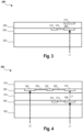
- Fig. 3 is a schematic illustration of a data processing component 200 (or part thereof) according to the first aspect of the present invention, in order to illustrate a high-level implementation of the invention.
- the data processing component comprises three layers: a substrate layer 202, a first logic layer 204, and a second logic layer 206.
- the substrate layer 202, first logic layer 204, and second logic layer are all planar, and parallel, but this need not be the case.
- the first logic layer 204 is formed on the substrate layer 202
- the second logic layer 206 is formed on the first logic layer 204.
- first logic layer 204 there may be intervening layers between the substrate layer 202 and the first logic layer 204, and/or between the first logic layer 204 and the second logic layer 206.
- the relative thicknesses of the substrate layer 202, first logic layer 204, and second logic layer 206 is also arbitrarily selected in Fig. 3 , and should in no way be construed as limiting.
- the first logic layer comprises a first data processing element 208, which is connected to a first comparator 210 via an electrical trace 212.
- the first data processing element 208 is configured to execute a predetermined operation on incoming data.
- the first data processing element is configured to execute the predetermined operation on a control input (not shown).
- the control input is a fixed input which is unrelated to the "real" data which is processed by the data processing component 200.
- the output of the predetermined operation on the control input is referred to herein as a first control output, which is transmitted to the first comparator 210 via the electrical trace 212.
- the first comparator 210 is then configured to compare the first control output with an expected control output, which is the expected output resulting from the execution of the predetermined operation on the control input.
- the first comparator 210 may retrieve the expected control output from a memory or other appropriate storage component, or may receive it from another component (not shown) within the first logic layer 204. If the first comparator 210 determines that the control output is different from the expected control output, the first comparator 210 is configured to output a fault status signal (e.g. in the form of a predetermined voltage signal). If there is no difference detected by the first comparator 210 between the control output and the expected control output, no fault status signal is generated. In some cases, a normal status signal may be generated and output.
- a fault status signal e.g. in the form of a predetermined voltage signal
- the second logic layer 206 includes a second data processing element 214.
- the second data processing element 214 is identical to the first data processing element 208, and crucially is configured to execute an identical predetermined operation.
- the second data processing element 214 is configured to receive a first operational input (not shown) and to execute the predetermined operation on it, to generate a first operational output.
- the first operational input differs from the control input in that it comprises real data, i.e. the second data processing element 214 is used to perform the real processing of data on the data processing component 200.
- the data processing component may optionally comprise power lines at a front side and a back side of a wafer.
- Fig. 3 shows a fault attack, in which electromagnetic radiation, for example in the form of laser light L1 of a selected wavelength is incident on the data processing component 200.
- the arrangement of data processing component 200 provides at least two means of defence against the fault attack:
- Fig. 4 illustrates schematic arrangement of components in a data processing component 300, which is able to offer effective protection against sophisticated fault attacks in which laser light is directed at the data processing component 300 in an attempt to induce the same fault in two identical data processing components, so that a comparator is not able to detect a difference in their outputs, and the fault goes undetected.
- the data processing component comprises five layers: a substrate layer 302, a first logic layer 304, an intervening layer 316, a second logic layer 306, and a shield layer 318.
- the substrate layer 302, first logic layer 304, intervening layer 316, second logic layer 306, and shield layer 318 are all planar, and parallel, but this need not be the case.
- the first logic layer 304 is formed on the substrate layer 302.
- the intervening layer 316 which may be a memory layer such as a RAM layer, is formed on the first logic layer 304.
- the second layer 306 is formed on the intervening layer 316.
- the shield layer 318 is formed on the second layer 306.
- the first logic layer 304 comprises a first data processing element 308.
- the first data processing element 308 is configured to execute a predetermined operation on incoming data.
- the first data processing element is configured to execute the predetermined operation on a control input (not shown).
- the control input is a fixed input which is unrelated to the "real" data which is processed by the data processing component 300.
- the output of the predetermined operation on the control input is referred to herein as a first control output, which is transmitted to the first comparator 310 via the electrical trace 312.
- the first comparator 310 is then configured to compare the first control output with an expected control output, which is the expected output resulting from the execution of the predetermined operation on the control input.
- the first comparator 310 may retrieve the expected control output from a memory or other appropriate storage component, or may receive it from another component (not shown) within the first logic layer 304. If the first comparator 310 determines that the control output is different from the expected control output, the first comparator 310 is configured to output a fault status signal (e.g. in the form of a predetermined voltage signal). If there is no difference detected by the first comparator 310 between the control output and the expected control output, no fault status signal is generated. In some cases, a normal status signal may be generated and output.
- a fault status signal e.g. in the form of a predetermined voltage signal
- the second logic layer 306 of the data processing component 300 is slightly different from the second logic layer 206 of data processing component 200.
- the second logic layer 306 includes a second data processing element 314.
- the second data processing element 314 is identical to the first data processing element 308, and crucially is configured to execute an identical predetermined operation.
- the second data processing element 314 is configured to receive a first operational input (not shown) and to execute the predetermined operation on it, to generate a first operational output.
- the first operational input differs from the control input in that it comprises real data, i.e. the second data processing element 314 is used to perform the real processing of data on the data processing component 300.
- the second logic layer 306 further comprises a third data processing element 320.
- the third data processing element 320 is identical to the first data processing element 308 and the second data processing element 314, and is configured to execute an identical predetermined operation as the two.
- the third data processing element 320 is configured to receive a second operational input (not shown) which is identical to the first operational input (e.g. from the same source) and to execute the predetermined operation on it, to generate a second operational output.
- the second operational input differs from the control input in that it comprises real data, i.e. the second data processing element 320 is also used to perform the real processing of data on the data processing component 300.
- the second logic layer 306 further comprises a second comparator 322, which is connected to the second data processing element 314 via electrical trace 326 and the third data processing element 320 via electrical trace 324.
- the second comparator 322 is then configured to compare the first operational output received from the second data processing element 314 with the second operational output received from the third data processing element 320. If the second comparator 322 determines that the control output is different from the second operational output, the second comparator 322 is configured to output a fault status signal (e.g. in the form of a predetermined voltage signal). If there is no difference detected by the second comparator 322 between the first operational output and the second operational output, no fault status signal is generated. In some cases, a normal status signal may be generated and output.
- a fault status signal e.g. in the form of a predetermined voltage signal
- Fig. 4 illustrates a fault attack in which, in which electromagnetic radiation, for example in the form of laser light L1 and laser light L2 of a selected wavelength are incident on the data processing component 300.
- the arrangement of data processing component 300 provides at least two means of defence against the fault attack:
- implementations of the data processing components 200, 300 enable the detection of fault attacks of varying levels of sophistication.
Landscapes
- Engineering & Computer Science (AREA)
- Theoretical Computer Science (AREA)
- Computer Security & Cryptography (AREA)
- Physics & Mathematics (AREA)
- Software Systems (AREA)
- General Engineering & Computer Science (AREA)
- General Physics & Mathematics (AREA)
- Computer Hardware Design (AREA)
- Quality & Reliability (AREA)
- Mathematical Physics (AREA)
- Storage Device Security (AREA)
- Executing Machine-Instructions (AREA)
Priority Applications (4)
| Application Number | Priority Date | Filing Date | Title |
|---|---|---|---|
| EP23192017.4A EP4510023A1 (de) | 2023-08-17 | 2023-08-17 | Datenverarbeitungskomponente und computerprozessor |
| TW113130528A TW202516383A (zh) | 2023-08-17 | 2024-08-14 | 資料處理構件及電腦處理器 |
| PCT/EP2024/072947 WO2025036955A1 (en) | 2023-08-17 | 2024-08-14 | Data processing component and computer processor |
| CN202480059591.1A CN121889795A (zh) | 2023-08-17 | 2024-08-14 | 数据处理组件和计算机处理器 |
Applications Claiming Priority (1)
| Application Number | Priority Date | Filing Date | Title |
|---|---|---|---|
| EP23192017.4A EP4510023A1 (de) | 2023-08-17 | 2023-08-17 | Datenverarbeitungskomponente und computerprozessor |
Publications (1)
| Publication Number | Publication Date |
|---|---|
| EP4510023A1 true EP4510023A1 (de) | 2025-02-19 |
Family
ID=87696032
Family Applications (1)
| Application Number | Title | Priority Date | Filing Date |
|---|---|---|---|
| EP23192017.4A Pending EP4510023A1 (de) | 2023-08-17 | 2023-08-17 | Datenverarbeitungskomponente und computerprozessor |
Country Status (4)
| Country | Link |
|---|---|
| EP (1) | EP4510023A1 (de) |
| CN (1) | CN121889795A (de) |
| TW (1) | TW202516383A (de) |
| WO (1) | WO2025036955A1 (de) |
Citations (3)
| Publication number | Priority date | Publication date | Assignee | Title |
|---|---|---|---|---|
| US20160072621A1 (en) * | 2014-09-05 | 2016-03-10 | Renesas Electronics Corporation | Semiconductor device |
| US20210342488A1 (en) * | 2012-11-09 | 2021-11-04 | Crossbar, Inc. | Secure circuit integrated with memory layer |
| US20230222251A1 (en) * | 2020-07-10 | 2023-07-13 | Nagravision Sàrl | Integrated circuit device with protection against malicious attacks |
-
2023
- 2023-08-17 EP EP23192017.4A patent/EP4510023A1/de active Pending
-
2024
- 2024-08-14 TW TW113130528A patent/TW202516383A/zh unknown
- 2024-08-14 CN CN202480059591.1A patent/CN121889795A/zh active Pending
- 2024-08-14 WO PCT/EP2024/072947 patent/WO2025036955A1/en active Pending
Patent Citations (3)
| Publication number | Priority date | Publication date | Assignee | Title |
|---|---|---|---|---|
| US20210342488A1 (en) * | 2012-11-09 | 2021-11-04 | Crossbar, Inc. | Secure circuit integrated with memory layer |
| US20160072621A1 (en) * | 2014-09-05 | 2016-03-10 | Renesas Electronics Corporation | Semiconductor device |
| US20230222251A1 (en) * | 2020-07-10 | 2023-07-13 | Nagravision Sàrl | Integrated circuit device with protection against malicious attacks |
Also Published As
| Publication number | Publication date |
|---|---|
| WO2025036955A1 (en) | 2025-02-20 |
| TW202516383A (zh) | 2025-04-16 |
| CN121889795A (zh) | 2026-04-17 |
Similar Documents
| Publication | Publication Date | Title |
|---|---|---|
| US12361136B2 (en) | Identification of a resource attack path by connecting code, configuration, and telemetry | |
| CN113597747B (zh) | 用于故障注入攻击的检测和定位的设备和方法 | |
| US8677482B2 (en) | Hardware security for software processes | |
| US8127360B1 (en) | Method and apparatus for detecting leakage of sensitive information | |
| CN112930659B (zh) | 用于安全密钥生成的方法和设备 | |
| Vashistha et al. | Toshi-towards secure heterogeneous integration: Security risks, threat assessment, and assurance | |
| EP3147830B1 (de) | Schutz fuer eine integrierte schaltung | |
| US10642947B2 (en) | System, method and computer-accessible medium providing secure integrated circuit camouflaging for minterm protection | |
| Busari | Secure Boot and Firmware Authentication Policies in SoCs | |
| CN120162837A (zh) | Mcu的信息保护方法、装置、电子设备及可读存储介质 | |
| Hamdioui et al. | Hacking and protecting IC hardware | |
| Singh | Securing Transactional Integrity: Cybersecurity Practices in Fintech and Core Banking | |
| EP4510023A1 (de) | Datenverarbeitungskomponente und computerprozessor | |
| KR20260053373A (ko) | 데이터 처리 부품 및 컴퓨터 프로세서 | |
| Edara et al. | Localization of Data Compromised by Hardware Attacks in Machine Learning Enabled Cyber-Physical Edge Devices | |
| Rajendran | Security challenges in hardware used for smart environments | |
| Lackner et al. | A defensive java card virtual machine to thwart fault attacks by microarchitectural support | |
| Pahuja et al. | Machine Learning-Based Detection and Mitigation of XML SQL Injection Attacks | |
| Chaurasia et al. | SecureHD: Designing low-cost reliable and security aware hardware accelerators during high-level synthesis for computationally intensive application frameworks | |
| US20160344753A1 (en) | Method for instruction set morphing to inhibit malicious code injection | |
| Timiş et al. | Triggering detection technique of the hardware trojans in the combinational logic systems | |
| Patil et al. | Hardware Security and Trusted Integrated Circuit (Ic) Design: Ensuring Reliability, Resilience, And Integrity in The Era of Semiconductor Globalization | |
| Timis et al. | Classification overview of the Hardware Trojans in digital circuits | |
| Pradesh et al. | Detection and Mitigation of Insider Attacks in Financial Systems | |
| Babenko et al. | Instrumental system for analysis of information systems using smart cards protection |
Legal Events
| Date | Code | Title | Description |
|---|---|---|---|
| PUAI | Public reference made under article 153(3) epc to a published international application that has entered the european phase |
Free format text: ORIGINAL CODE: 0009012 |
|
| STAA | Information on the status of an ep patent application or granted ep patent |
Free format text: STATUS: THE APPLICATION HAS BEEN PUBLISHED |
|
| AK | Designated contracting states |
Kind code of ref document: A1 Designated state(s): AL AT BE BG CH CY CZ DE DK EE ES FI FR GB GR HR HU IE IS IT LI LT LU LV MC ME MK MT NL NO PL PT RO RS SE SI SK SM TR |
|
| STAA | Information on the status of an ep patent application or granted ep patent |
Free format text: STATUS: REQUEST FOR EXAMINATION WAS MADE |
|
| 17P | Request for examination filed |
Effective date: 20250819 |