EP4510030A1 - Dispositif logique et système et procédés de définition et de configuration d'un dispositif logique - Google Patents
Dispositif logique et système et procédés de définition et de configuration d'un dispositif logique Download PDFInfo
- Publication number
- EP4510030A1 EP4510030A1 EP23306382.5A EP23306382A EP4510030A1 EP 4510030 A1 EP4510030 A1 EP 4510030A1 EP 23306382 A EP23306382 A EP 23306382A EP 4510030 A1 EP4510030 A1 EP 4510030A1
- Authority
- EP
- European Patent Office
- Prior art keywords
- memory cells
- programme
- address space
- definition
- gate array
- Prior art date
- Legal status (The legal status is an assumption and is not a legal conclusion. Google has not performed a legal analysis and makes no representation as to the accuracy of the status listed.)
- Pending
Links
Images



Classifications
-
- G—PHYSICS
- G06—COMPUTING OR CALCULATING; COUNTING
- G06F—ELECTRIC DIGITAL DATA PROCESSING
- G06F21/00—Security arrangements for protecting computers, components thereof, programs or data against unauthorised activity
- G06F21/70—Protecting specific internal or peripheral components, in which the protection of a component leads to protection of the entire computer
- G06F21/71—Protecting specific internal or peripheral components, in which the protection of a component leads to protection of the entire computer to assure secure computing or processing of information
- G06F21/76—Protecting specific internal or peripheral components, in which the protection of a component leads to protection of the entire computer to assure secure computing or processing of information in application-specific integrated circuits [ASIC] or field-programmable devices, e.g. field-programmable gate arrays [FPGA] or programmable logic devices [PLD]
-
- G—PHYSICS
- G11—INFORMATION STORAGE
- G11C—STATIC STORES
- G11C29/00—Checking stores for correct operation ; Subsequent repair; Testing stores during standby or offline operation
- G11C29/04—Detection or location of defective memory elements, e.g. cell constructio details, timing of test signals
- G11C29/08—Functional testing, e.g. testing during refresh, power-on self testing [POST] or distributed testing
- G11C29/12—Built-in arrangements for testing, e.g. built-in self testing [BIST] or interconnection details
- G11C29/38—Response verification devices
-
- G—PHYSICS
- G06—COMPUTING OR CALCULATING; COUNTING
- G06F—ELECTRIC DIGITAL DATA PROCESSING
- G06F15/00—Digital computers in general; Data processing equipment in general
- G06F15/76—Architectures of general purpose stored program computers
- G06F15/78—Architectures of general purpose stored program computers comprising a single central processing unit
- G06F15/7867—Architectures of general purpose stored program computers comprising a single central processing unit with reconfigurable architecture
- G06F15/7871—Reconfiguration support, e.g. configuration loading, configuration switching, or hardware OS
-
- G—PHYSICS
- G06—COMPUTING OR CALCULATING; COUNTING
- G06F—ELECTRIC DIGITAL DATA PROCESSING
- G06F13/00—Interconnection of, or transfer of information or other signals between, memories, input/output devices or central processing units
- G06F13/14—Handling requests for interconnection or transfer
- G06F13/16—Handling requests for interconnection or transfer for access to memory bus
- G06F13/1605—Handling requests for interconnection or transfer for access to memory bus based on arbitration
- G06F13/1647—Handling requests for interconnection or transfer for access to memory bus based on arbitration with interleaved bank access
-
- G—PHYSICS
- G06—COMPUTING OR CALCULATING; COUNTING
- G06F—ELECTRIC DIGITAL DATA PROCESSING
- G06F13/00—Interconnection of, or transfer of information or other signals between, memories, input/output devices or central processing units
- G06F13/14—Handling requests for interconnection or transfer
- G06F13/16—Handling requests for interconnection or transfer for access to memory bus
- G06F13/1668—Details of memory controller
-
- G—PHYSICS
- G06—COMPUTING OR CALCULATING; COUNTING
- G06F—ELECTRIC DIGITAL DATA PROCESSING
- G06F15/00—Digital computers in general; Data processing equipment in general
- G06F15/76—Architectures of general purpose stored program computers
- G06F15/78—Architectures of general purpose stored program computers comprising a single central processing unit
- G06F15/7867—Architectures of general purpose stored program computers comprising a single central processing unit with reconfigurable architecture
- G06F15/7885—Runtime interface, e.g. data exchange, runtime control
-
- G—PHYSICS
- G06—COMPUTING OR CALCULATING; COUNTING
- G06F—ELECTRIC DIGITAL DATA PROCESSING
- G06F21/00—Security arrangements for protecting computers, components thereof, programs or data against unauthorised activity
- G06F21/10—Protecting distributed programs or content, e.g. vending or licensing of copyrighted material ; Digital rights management [DRM]
- G06F21/16—Program or content traceability, e.g. by watermarking
-
- G—PHYSICS
- G06—COMPUTING OR CALCULATING; COUNTING
- G06F—ELECTRIC DIGITAL DATA PROCESSING
- G06F21/00—Security arrangements for protecting computers, components thereof, programs or data against unauthorised activity
- G06F21/60—Protecting data
- G06F21/64—Protecting data integrity, e.g. using checksums, certificates or signatures
-
- G—PHYSICS
- G11—INFORMATION STORAGE
- G11C—STATIC STORES
- G11C29/00—Checking stores for correct operation ; Subsequent repair; Testing stores during standby or offline operation
- G11C29/04—Detection or location of defective memory elements, e.g. cell constructio details, timing of test signals
- G11C29/08—Functional testing, e.g. testing during refresh, power-on self testing [POST] or distributed testing
- G11C29/12—Built-in arrangements for testing, e.g. built-in self testing [BIST] or interconnection details
- G11C29/1201—Built-in arrangements for testing, e.g. built-in self testing [BIST] or interconnection details comprising I/O circuitry
-
- H—ELECTRICITY
- H03—ELECTRONIC CIRCUITRY
- H03K—PULSE TECHNIQUE
- H03K19/00—Logic circuits, i.e. having at least two inputs acting on one output; Inverting circuits
- H03K19/02—Logic circuits, i.e. having at least two inputs acting on one output; Inverting circuits using specified components
- H03K19/173—Logic circuits, i.e. having at least two inputs acting on one output; Inverting circuits using specified components using elementary logic circuits as components
- H03K19/177—Logic circuits, i.e. having at least two inputs acting on one output; Inverting circuits using specified components using elementary logic circuits as components arranged in matrix form
- H03K19/17724—Structural details of logic blocks
- H03K19/17728—Reconfigurable logic blocks, e.g. lookup tables
Definitions
- the present invention relates to logic devices such as field programmable gate array devices, ASICs, and other such devices.
- FPGAs are a type of Programmable Logic Device. They are generally based on a standard programmable Logic Block, a large number of which are arranged together to implement various functions.
- FIG 1 shows schematically an example of an FPGA system as known in the state of the art.
- an FPGA chip 10 comprises a number of Logic Blocks 11, for example as described above.
- the chip also comprises a number of input/output ports 12. Connecting these logic blocks 11 and input/output ports 12 are a number of tracks 14. At junction points of these tracks are provided and number of programmable routing areas 13. In these programmable routing areas there are provided switches which can selectively connect any pair of intersecting tracks, under the control of a logical value stored in a memory cell connected with each switch.
- the switch memory values are set at system start up from a non volatile memory. Accordingly, by setting the values in the switch memories as required, any connections of any Logic Block can be coupled to those of any other Logic Block, or any input/output port 12.
- any desired functionality can be implemented.
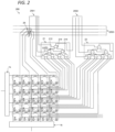
- FIG. 2 shows further detail of elements of an FPGA system as known in the state of the art.
- figure 2 constitute a representative example of a partial implementation of parts of the functionality described above with respect to figure 1 .
- the first LUT 21 comprises seven two input multiplexers 211, 212, 213, 214, 215, 216, 217 respectively.
- the second LUT and further LUTs are configured similarly. These multiplexers are arranged in a cascading manner with three rows so as to constitute an 8 input multiplexer, the output of which constitutes the output of the LUT.
- the first row of multiplexers (211, 213, 215 and 217) in each cascade arrangement both have a total of eight inputs. These eight inputs constitute the programming inputs of the first LUT 21.
- the selection inputs of each row are ganged together, to constitute the three data inputs of the LUT.
- the data inputs and data output of the first LUT are connected to a set of tracks 2501, 2502.
- the inputs and outputs of the second and further LUTs are connected correspondingly to a network of further tracks (not shown).
- a LUT with 3 data inputs in this manner is referred to as a "LUT3”.
- Each of the eight programming inputs of the first LUT 21 connected to a respective Static RAM memory device 251, 252, 253, 254, 255, 256, 257, 258.
- Corresponding memory devices provide the configuration inputs of the second LUT 22, and the other LUTs provided in the system (not shown).
- Dynamic RAM devices may also comprise Static RAM devices.
- these memory devices 2a, 2b, 2c, 2d, 2e, 2f, 2g, 2h, 2i, 2j, 2k, 2l, 2m, 2n, 2o, 2p, 2q, 2r, 2s, 2t, 2u, 2v, 2w, 2x, 2y, 2z provide a constant predetermined logical value to each of the eight programming inputs of each LUT.
- each memory cell is shown schematically as comprising a latch built of two inverters, each receiving the output of the other, with a transistor switch, switched by a word line 23, provided to enable the selective output of the value on the output of one of the inverters in the latch to a bit line connected to a respective configuration input of the LUT 217, and also to a data line 24 by means of which the value of the latch may be set.
- each memory device 2g, 2h, 2i, 2j, 2k, 2l, 2m, 2n, 2o, 2p, 2q, 2r, 2s, 2t, 2u, 2v, 2w, 2x, 2y, 2z, is connected to a row decoder 1a and the word line of each memory device 251, 252, 253, 254, 255, 256, 257, 258 is connected to a line decoder 1b.
- each memory device 2a, 2b, 2c, 2d, 2e, 2f, 2g, 2h, 2i, 2j, 2k, 2l, 2m, 2n, 2o, 2p, 2q, 2r, 2s, 2t, 2u, 2v, 2w, 2x, 2y, 2z, is addressed in turn, and the desired value set to the latch in question.
- the logical behaviour of the LUT is response to any binary value on its three data inputs can thus be defined as required. This is the underlying basic concept of FPGA technology.
- a single Logic block comprising two LUT3s can implement is limited, however by interconnecting a number of suitably configured LUTs as described above, any arbitrary combinatorial function can be implemented.
- This interconnection is achieved through a programmable interconnection of the data channels 2501, 2502, and further channels (not shown) carrying data from other LUTs.
- channels 2501, 2502 are arranged vertically, there is provided a further channel 2503 intersecting channels 2501, 2502.
- a programmable switching unit 26 At the intersection of respective lines of channels 2501 and 2503 is provided a programmable switching unit 26.
- the switching unit comprises 6 transistor switches, arranged to make or break a connection between any two of these four connections.
- Each of these transistor switches is set to be open or closed by a value received from a respective static memory unit 2a, 2b, 2c, 2d, 2e, 2f.
- static memory unit 2a, 2b, 2c, 2d, 2e, 2f Further such programmable switching units, with corresponding static memory devices are provided at many or all intersection of tracks (not shown).
- static memory devices 2a, 2b, 2c, 2d, 2e, 2f are identical to the memory devices 2g, 2h, 2i, 2j, 2k, 2l, 2m, 2n, 2o, 2p, 2q, 2r, 2s, 2t, 2u, 2v, 2w, 2x, 2y, 2z,and connected to the decoder matrix 1a, 1b, so that when during an initiation phase for the circuit, both the LUT memory devices and switch memory devices may be addressed in turn, and the desired value set to the latch in question, so that the behaviour of each LUT, and its connections to any other LUT may be configured as required.
- WO2012/123243 A1 , US7463056 B1 , US6021513 A , US5432441 A , US8091001 B2 , US5675589 A , and US5027355 A describe certain aspects of the foregoing.
- the structure thus defined is highly flexible, and can be reprogrammed and revised at various levels, e.g. hardware and software (configuration values), at different times, so that it can become difficult to determine unambiguously which configuration version a particular device implements.
- IP Intelligent Property
- a computer implemented method of defining a device capable of implementing a logic function comprising a memory bus having a corresponding address space, and a plurality of programme memory cells, each programme memory cell being accessible for reading and/or writing via the memory bus with a respective address in the address space, wherein the device further comprises a plurality of auxiliary memory cells, each auxiliary memory cell being accessible for reading via the programme memory bus with a respective address in the address space, the select lines and/or outputs of each lookup table being programmably interconnected with the select lines or outputs of another lookup table independently of the respective values of the plurality of auxiliary memories, the method comprising obtaining a checksum value for the digital definition of logic function, finding a digital value of a predefined length which, when applied to a package checksum value comprising the checksum value for the digital definition of core functions, in accordance with a predefined operation, produces a result complying with a predefined rule, and defining an
- the step of finding a digital value of a predefined length comprises testing successive random digital values of a predefined length against the predefined rule until a digital value of a predefined length which, when applied to a package checksum value comprising the checksum value for the digital definition of core functions, in accordance with a predefined operation, produces a result complying with a predefined rule is found.
- the method comprises the further step incorporating a historical checksum from a preceding iteration of the method of the first aspect to the package checksum by a predetermined operation before the step of finding a digital value of a predefined length.
- the method comprises the further step of encrypting the augmented digital definition of the Field Programmable Gate Array.
- the method comprises the further step of defining a bitstream with regard to the address space such that when the bitstream is loaded into the programme memories the Field Programmable Gate Array implement a defined logic function.
- the method comprises the further step loading the bitstream into the programme memories so as to program the Field Programmable Gate Array to implement the defined logic function.
- a method of interrogating a Field Programmable Gate Array defined in accordance with the first aspect, the method of interrogating comprising the step of reading the contents of the auxiliary memory cells in a sequence defined as a function of the memory space.
- some or all of the programme memory cells are configured to output their values to one or more shift registers, and wherein the step of step of reading the contents of the auxiliary memory cells comprises clocking the one or more shift registers in a predefined sequence to read out their contents, wherein the step of reading the contents of the auxiliary memory cells in a sequence defined as a function of the memory space comprises interleaving the contents of the auxiliary memory cells with the contents read from the shift registers to achieve a predefined output structure.
- a device defined in accordance with the method of the first aspect.
- a computer program comprising instructions which, when the program is executed by a computer, cause the computer to carry out the method of the first aspect.
- a computer-readable medium storing data defining a defined in accordance with the method of the first aspect.
- Field Programmable Gate Array capable of implementing a logic function
- the Field Programmable Gate Array comprising a plurality of hardware lookup tables each comprising a plurality of select lines and/or outputs, a programme memory bus having a corresponding address space, and a plurality of programme memory cells, each programme memory cell being accessible for reading and/or writing via the programme memory bus with a respective address in the address space, the select lines and/or outputs of each lookup table being programmably interconnected with the select lines or outputs of another lookup table dependent on the respective values of the plurality of programme memories
- the Field Programmable Gate Array further comprises a plurality of auxiliary memory cells, each auxiliary memory cell being accessible for reading via the programme memory bus with a respective address in the address space, the select lines and/or outputs of each lookup table being programmably interconnected with the select lines or outputs of another lookup table independently of the respective values of the plurality of auxiliary memories.
- one or more auxiliary memory cells returns a fixed value defined in hardware.
- the address space is defined by values in two dimensions, and wherein the addresses in the address space via which the one or more auxiliary memory cells are accessible belong to a continuous region including the minimum value in each dimension of the address space and/or a continuous region including the maximum value in each dimension of the address space.
- one or more auxiliary memory cells stores a watermark value, and unique identifier or a version reference.
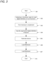
- Figure 3 presents a computer implemented method of defining a Logic device
- a logic device may generally be defined with reference to a digital definition of core functions thereof, e.g. in terms of an "IP" as discussed above.
- a method starts at step3 before proceeding to a step 302 of obtaining a checksum value for the digital definition of core functions.
- a suitable checksum may be obtained by any suitable algorithm as will readily occur to the skilled person, such as Parity byte or parity word, Sum complement, cyclic redundancy checks, or indeed hash algorithms such as MD5 or SHA256 hashes.
- step 303 of finding a digital value of a predefined length which, when applied to the checksum value obtained at step 302 produces a result complying with a predefined rule.
- This number may be obtained by successively generating random numbers until one satisfying the specified conditions is found.
- the predefined length may be a convenient number of bits, which as will become clear from the following discussion may be equal to, or less than, the number of auxiliary memory cells provided by the logic device.
- a rule may be any rule that may be applied to a digital value, such as, for example: "The number must be an odd number”, “The number must be an even number”, “the number must be a prime number”, “the number must be a multiple of some other predefined number”, “the number digits at odd locations must be all odd” “the number digits at odd locations must be all odd even”,” part of the number may compare true to a predefined string", etc.
- a rule may comprise a combination of such requirements.
- the checksum value obtained at step 303 may be augmented with additional data.
- a historical checksum for example from a preceding iteration of the method of figure 4 , may be incorporated into the checksum value obtained at step 303 by a predetermined operation.
- the previous checksum is kept on a file which is also included into the package files list of the current checksum being computed. This will create the chain.
- the checksum can be seen to constitute a "blockchain", tying the obtained value to only to its current version, but also to every subsequent version in a series of iterations of the described method.
- the step of finding a digital value of a predefined length may optionally be implemented by testing successive random digital values of a predefined length against the predefined rule until a digital value of a predefined length which, when applied to a package checksum value comprising the checksum value for the digital definition of core functions, in accordance with a predefined operation, produces a result complying with the predefined rule is found.th.
- embodiments may relate to the definition of any logic device, certain embodiments may be particularly convenient as applied to programmable devices such as FPGAs as discussed above, where the logical function is not defined (exclusively) by the device architecture, but primarily by a bitstream that may be loaded into the device after manufacture. Embodiments may relate to the definition of such a bitstream.
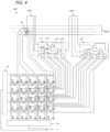
- Figure 4 presents a logic device suitable for definition in accordance with certain embodiments.
- FIG 4 there is presented a Field Programmable Gate Array 400. Certain elements of the Field Programmable Gate Array 400 correspond to those of Field Programmable Gate Array 200 described with reference to figure 2 , and like numbered elements may be considered to correspond, and may not be further described. As will be apparent to the skilled person, the logic function may be any set of operations consistent with the capacity of the FPGA structure.
- the Field Programmable Gate Array 400 comprises a plurality of hardware lookup tables 21, 21 each comprising a plurality of select lines and/or outputs 2501, 2502, 2503, a programme memory bus 1 having a corresponding address space, and a plurality of programme memory cells 2a, 2b, 2c, 2d, 2e, 2f, 2g, 2h, 2i, 2j, 2k, 2l, 2m, 2n, 2o, 2p, 2q, 2r, 2y, each programme memory cell being accessible for reading and/or writing via the programme memory bus 1a, 1b, with a respective address in the address space.
- select lines and/or outputs 2501, 2502, 2503 of each lookup table are programmably interconnectable with the select lines or outputs 2501, 2502, 2503 of other lookup tables dependent on the respective values of the plurality of programme memories, e.g. through the memory controlled operation of switch 26.
- the Field Programmable Gate Array further comprises a plurality of auxiliary memory cells 4a, 4b, 4c, 4d, each auxiliary memory cell being accessible for reading via the programme memory bus with a respective address in the address space.
- each lookup table being programmably interconnected with the select lines or outputs of another lookup table independently of the respective values of the plurality of auxiliary memories- that is to say, the auxiliary memory cells 4a, 4b, 4c, 4d while addressable in the same address space as the programme memory cells 2a, 2b, 2c, 2d, 2e, 2f, 2g, 2h, 2i, 2j, 2k, 2l, 2m, 2n, 2o, 2p, 2q, 2r, 2y do not serve to configure the FPGA device, but remain available for other uses.
- auxiliary memory cells may be programmed with any arbitrary value which may be required for future reference, such as a watermark value, an unique identifier or a version reference or the like. While only four auxiliary memory cells are provided in figure 4 , real implementations may comprise any number of cells as may be required depending on the auxiliary data to be stored.
- figure 4 presents a device capable of implementing a logic function, the device comprising a memory bus having a corresponding address space, and a plurality of programme memory cells, each programme memory cell being accessible for reading and/or writing via the memory bus with a respective address in the address space, wherein the device further comprises a plurality of auxiliary memory cells, each auxiliary memory cell being accessible for reading via the programme memory bus with a respective address in the address space, the select lines and/or outputs of each lookup table being programmably interconnected with the select lines or outputs of another lookup table independently of the respective values of the plurality of auxiliary memories.
- a Field Programmable Gate Array capable of implementing a logic function
- the Field Programmable Gate Array comprising a plurality of hardware lookup tables each comprising a plurality of select lines and/or outputs, a programme memory bus having a corresponding address space, and a plurality of programme memory cells, each programme memory cell being accessible for reading and/or writing via the programme memory bus with a respective address in the address space, the select lines and/or outputs of each lookup table being programmably interconnected with the select lines or outputs of another lookup table dependent on the respective values of the plurality of programme memories
- the Field Programmable Gate Array further comprises a plurality of auxiliary memory cells, each auxiliary memory cell being accessible for reading via the programme memory bus with a respective address in the address space, the select lines and/or outputs of each lookup table being programmable interconnected with the select lines or outputs of another lookup table independently of the respective values of the plurality of auxiliary memories.
- the method may then proceed to an optional step 306 of defining a bitstream with regard to the address space of the Logic device such that when the bitstream is loaded into the programme memories of the Field Programmable Gate Array implement a defined logic function.
- the method may then proceed to step 307 at which the bitstream obtained at step 306 may then be loaded into the programme memories of the Logic device so as to program the Logic device to implement the defined logic function, and to store the digital value of a predefined length in the auxiliary memory cells of the logic device.
- Figure 5 presents a logic device suitable for definition in accordance with certain further embodiments.
- Figure 5 corresponds to figure 4 as regards the elements in common with figure 2 .
- a Field Programmable Gate Array comprises a plurality of auxiliary memory cells 5a, 5b, 5c, 5d.
- each of the auxiliary memory cells are configured to return a fixed value defined in hardware.
- the data gate of the memory access transistor of auxiliary memories 5a and 5c is simply tied to the positive voltage rail, while the data gate of the memory access transistor of auxiliary memories 5b and 5d is tied to ground.
- auxiliary memory cells may be programmed with any arbitrary value which may be required for future reference, such as a watermark value, a unique identifier or a version reference or the like. While only four auxiliary memory cells are provided in figure 5 , real implementations may comprise any number of cells as may be required depending on the auxiliary data to be stored.
- Figure 5 additionally provides latch structures 50a, 50b at the output of each Lookup table.
- these structures each comprise a multiplexer receiving an input either from the output of a respective LUT, or from a preceding latch structure, and providing an input to a respective D flip flop, the output of which is provided to an output bus 2501, 2502, and to an input of the multiplexer in the next latch structure.
- a shift register configuration may be defined whereby the outputs of the respective LUTS may be read out.
- auxiliary memory addresses In other types of Logic device, other mechanisms for reading the contents of the auxiliary memory addresses may be provided.
- the address space is defined by values in two dimensions, i.e. corresponding to rows and columns. It will be appreciated that other configurations are possible, for example based on a single linear address space. Such a linear address space may be programmable and/or accessible using a shift register or the like.
- the addresses in the address space via which the one or more auxiliary memory cells is accessible may be conveniently defined as belonging to one or more continuous regions including the minimum value in each dimension of the address space and/or a continuous region including the maximum value in each dimension of the address space.
- the Auxiliary memories may be conveniently defined at the edges and further still at the corners of the address space matrix.
- Typical FPGA bitstreams typically avoid these address combinations, so that these addresses may be set aside for the use as auxiliary memory cells with a minimal impact on the structure of the program bitstream for a given FPGA structure and logic function.
- steps 306 and 307 are dependent on a correct representation of the address space of the logic device, to ensure not only that the logic device is in fact correctly configured to implement the desired logic function, but also to load the required data into the auxiliary memory cells, in the desired sequence.
- a predefined logic device structure such as discussed with reference to figure 4 is to provide the substrate for the bitstream.
- the logic device structure itself may be variable and may indeed be defined as a function of the data to be loaded into it.
- the logic device structure may be defined, e.g. in terms of a semiconductor "IP", which may be converted using conventional industry practices into a semiconductor mask, for fabrication of corresponding logic device devices.
- the method implements an step 304 at which an augmented digital definition of the Field Programmable Gate Array is defined, comprising the digital definition of core functions and a definition of the one or more auxiliary memory cells reflecting the digital value of a predefined length.
- the augmented digital definition of the Field Programmable Gate Array obtained at step 304 may be encrypted. Encryption may protect the VHDL code making its duplication much trickier while the watermarking can prove the copy in case of violation is not genuine.
- a further step 305 of fabricating a logic device in accordance with the augmented digital definition may then be performed. As shown, these steps may be performed before steps 306 and 307 so that the logic device structure and underlying address space are formally defined so as to support the definition and loading of the bitstream.
- step 306 may be performed after or in parallel with step 304, in which case a particular memory space may be assumed for the generation of the bitstream, and then effectively integrated in the final structure, and that step 305 may be performed after or in parallel with step 306.
- the method then terminates at step 310.
- a computer implemented method of defining a device capable of implementing a logic function comprising a memory bus having a corresponding address space, and a plurality of programme memory cells, each programme memory cell being accessible for reading and/or writing via the memory bus with a respective address in the address space, wherein the device further comprises a plurality of auxiliary memory cells, each auxiliary memory cell being accessible for reading via the programme memory bus with a respective address in the address space, the select lines and/or outputs of each lookup table being programmably interconnected with the select lines or outputs of another lookup table independently of the respective values of the plurality of auxiliary memories, the method comprising obtaining a checksum value for the digital definition of the logic function, finding a digital value of a predefined length which, when applied to a package checksum value comprising the checksum value for the digital definition of core functions, in accordance with a predefined operation, produces a result complying with a predefined rule, and defining an augmented digital definition of the device thereof comprising obtaining a checksum value
- a logic device so defined provides additional information that may be retrieved from the auxiliary memory cells.
- a computer implemented method of interrogating a logic device comprising the step of reading the contents of the auxiliary memory cells in a sequence defined as a function of the memory space.
- a method of defining a logic device in which the definition incorporates the definition of special auxiliary memory cells reserved for the presentation of a special code, incorporating a signature of the definition as a whole so as to constitute a watermark securing the design as a whole, and possibly other information.
- the special code may incorporate recursively signatures from preceding versions of the same devices to as to constitute a watermark blockchain.
- a LUT based FPGA architecture is proposed with special addressable memory cells reserved for this purpose, in which case a programming bitstream may constitute a definition in accordance with the inventive method.
- the step of reading the contents of the auxiliary memory cells may comprise clocking the one or more shift registers in a predefined sequence to read out their contents.
- the step of reading the contents of the auxiliary memory cells in a sequence defined as a function of the memory space may comprises interleaving the contents of the auxiliary memory cells (as retrieved by a sequential addressing of the memory space as described above) with the contents read from the shift registers to achieve a predefined output structure.
- the disclosed implementations can take form of an entirely hardware embodiment (e.g. FPGA or logic device, for example as described above or obtained as a result of the method of figure 3 ), or as described with reference to figures 4 or 5 , an entirely software embodiment (for example implementing the method described with respect to figure 3 , or other methods presented herein) or an embodiment containing both hardware and software elements.
- Software embodiments include but are not limited to firmware, resident software, microcode, etc.
- the invention can take the form of a computer program product accessible from a computer-usable or computer-readable medium providing program code for use by or in connection with a computer or an instruction execution system.
- a computer-usable or computer-readable can be any apparatus that can contain, store, communicate, propagate, or transport the program for use by or in connection with the instruction execution system, apparatus, or device.
- the medium can be an electronic, magnetic, optical, electromagnetic, infrared, or semiconductor system (or apparatus or device) or a propagation medium.
- the methods and processes described herein may be implemented in whole or part by a user device. These methods and processes may be implemented by computer-application programs or services, an application-programming interface (API), a library, and/or other computer-program product, or any combination of such entities.
- API application-programming interface
- the user device may be a mobile device such as a smart phone or tablet, a computer or any other device with processing capability, such as a robot or other connected device.
- Figure 6 shows a generic computing system suitable for implementation of embodiments of the invention.
- a system includes a logic device 601 and a storage device 602.
- the system may optionally include a display subsystem 611, input subsystem 612, 613, 614, communication subsystem 620, and/or other components not shown.
- Logic device 601 includes one or more physical devices configured to execute instructions.
- the logic device 601 may be configured to execute instructions that are part of one or more applications, services, programs, routines, libraries, objects, components, data structures, or other logical constructs.
- Such instructions may be implemented to perform a task, implement a data type, transform the state of one or more components, achieve a technical effect, or otherwise arrive at a desired result.
- the logic device 601 may include one or more processors configured to execute software instructions. Additionally or alternatively, the logic device may include one or more hardware or firmware logic devices configured to execute hardware or firmware instructions. Processors of the logic device may be single-core or multi-core, and the instructions executed thereon may be configured for sequential, parallel, and/or distributed processing. Individual components of the logic device 601 optionally may be distributed among two or more separate devices, which may be remotely located and/or configured for coordinated processing. Aspects of the logic device 601 may be virtualized and executed by remotely accessible, networked computing devices configured in a cloud-computing configuration.
- Storage device 602 includes one or more physical devices configured to hold instructions executable by the logic device to implement the methods and processes described herein. When such methods and processes are implemented, the state of storage 602 device may be transformed-e.g., to hold different data.
- Storage device 602 may include removable and/or built-in devices.
- Storage device 602 may comprise one or more types of storage device including optical memory (e.g., CD, DVD, HD-DVD, Blu-Ray Disc, etc.), semiconductor memory (e.g., RAM, EPROM, EEPROM, etc.), and/or magnetic memory (e.g., hard-disk drive, floppy-disk drive, tape drive, MRAM, etc.), among others.
- Storage device may include volatile, non-volatile, dynamic, static, read/write, read-only, random-access, sequential-access, location-addressable, file-addressable, and/or content-addressable devices.
- the system may comprise an interface 603 adapted to support communications between the Logic device 601 and further system components.
- additional system components may comprise removable and/or built-in extended storage devices.
- Extended storage devices may comprise one or more types of storage device including optical memory 632 (e.g., CD, DVD, HD-DVD, Blu-Ray Disc, etc.), semiconductor memory 433 (e.g., RAM, EPROM, EEPROM, FLASH etc.), and/or magnetic memory 631 (e.g., hard-disk drive, floppy-disk drive, tape drive, MRAM, etc.), among others.
- Such extended storage device may include volatile, non-volatile, dynamic, static, read/write, read-only, random-access, sequential-access, location-addressable, file-addressable, and/or content-addressable devices.
- storage device includes one or more physical devices, and excludes propagating signals per se.
- aspects of the instructions described herein alternatively may be propagated by a communication medium (e.g., an electromagnetic signal, an optical signal, etc.), as opposed to being stored on a storage device.
- a communication medium e.g., an electromagnetic signal, an optical signal, etc.
- logic device 601 and storage device 402 may be integrated together into one or more hardware-logic components.
- Such hardware-logic components may include field-programmable gate arrays (FPGAs), program- and application-specific integrated circuits (PASIC/ASICs), program- and application-specific standard products (PSSP/ASSPs), system-on-a-chip (SOC), and complex programmable logic devices (CPLDs), for example.
- FPGAs field-programmable gate arrays
- PASIC/ASICs program- and application-specific integrated circuits
- PSSP/ASSPs program- and application-specific standard products
- SOC system-on-a-chip
- CPLDs complex programmable logic devices
- program may be used to describe an aspect of computing system implemented to perform a particular function.
- a program may be instantiated via logic device executing machine-readable instructions held by storage device. It will be understood that different modules may be instantiated from the same application, service, code block, object, library, routine, API, function, etc. Likewise, the same program may be instantiated by different applications, services, code blocks, objects, routines, APIs, functions, etc.
- program may encompass individual or groups of executable files, data files, libraries, drivers, scripts, database records, etc.
- system of figure 6 may be used to implement embodiments of the invention.
- a program implementing the steps described with respect to figure 5 may be stored in storage device 602 and executed by logic device 601.
- the Digital Definition, Checksum Value, Checksum Complement and/or Augmented Digital Definition may be stored in storage 602 or the extended storage devices 632, 633 or 631.
- the Logic device may determine any or all of the Digital Definition, Checksum Value, Checksum Complement and/or Augmented Digital Definition.
- display subsystem 611 may be used to present a visual representation of data held by storage device. This visual representation may take the form of a graphical user interface (GUI).
- GUI graphical user interface
- Display subsystem 611 may include one or more display devices utilizing virtually any type of technology. Such display devices may be combined with logic device and/or storage device in a shared enclosure, or such display devices may be peripheral display devices.
- the display 611 and user interface may be used to support CAD operations for the definition of the Digital definition, and so forth.
- the invention may be embodied in the form of a computer program.
- a “service”, as used herein, is an application program executable across multiple user sessions.
- a service may be available to one or more system components, programs, and/or other services.
- a service may run on one or more server-computing devices.
- input subsystem may comprise or interface with one or more user-input devices such as a keyboard 612, mouse 611, touch screen 611, or game controller, button, footswitch, etc. (not shown).
- user-input devices such as a keyboard 612, mouse 611, touch screen 611, or game controller, button, footswitch, etc. (not shown).
- the input subsystem may comprise or interface with selected natural user input (NUI) componentry.
- NUI natural user input
- Example NUI componentry may include a microphone for speech and/or voice recognition; an infrared, colour, stereoscopic, and/or depth camera for machine vision and/or gesture recognition; a head tracker, eye tracker 660, accelerometer, and/or gyroscope for motion detection and/or intent recognition; as well as electric-field sensing componentry for assessing brain activity.
- communication subsystem 620 may be configured to communicatively couple computing system with one or more other computing devices.
- communication module of may communicatively couple computing device to remote service hosted for example on a remote server 676 via a network of any size including for example a personal area network, local area network, wide area network, or the internet.
- Communication subsystem may include wired and/or wireless communication devices compatible with one or more different communication protocols.
- the communication subsystem may be configured for communication via a wireless telephone network 674, or a wired or wireless local- or wide-area network.
- the communication subsystem may allow computing system to send and/or receive messages to and/or from other devices via a network such as the Internet 675.
- the communications subsystem may additionally support short range inductive communications 621 with passive devices (NFC, RFID etc.).
- system of figure 6 is intended to reflect a broad range of different types of information handling system. It will be appreciated that many of the subsystems and features described with respect to figure 6 are not required for implementation of the invention, but are included to reflect possible systems in accordance with the present invention. It will be appreciated that system architectures vary widely, and the relationship between the different sub-systems of figure 6 is merely schematic, and is likely to vary in terms of layout and the distribution of roles in systems. It will be appreciated that, in practice, systems are likely to incorporate different subsets of the various features and subsystems described with respect to figure 6 .
Landscapes
- Engineering & Computer Science (AREA)
- Theoretical Computer Science (AREA)
- Physics & Mathematics (AREA)
- Computer Hardware Design (AREA)
- General Engineering & Computer Science (AREA)
- General Physics & Mathematics (AREA)
- Computer Security & Cryptography (AREA)
- Software Systems (AREA)
- Mathematical Physics (AREA)
- Computing Systems (AREA)
- Health & Medical Sciences (AREA)
- Bioethics (AREA)
- General Health & Medical Sciences (AREA)
- Multimedia (AREA)
- Technology Law (AREA)
- Microelectronics & Electronic Packaging (AREA)
- Logic Circuits (AREA)
Priority Applications (3)
| Application Number | Priority Date | Filing Date | Title |
|---|---|---|---|
| EP23306382.5A EP4510030A1 (fr) | 2023-08-16 | 2023-08-16 | Dispositif logique et système et procédés de définition et de configuration d'un dispositif logique |
| US18/798,515 US20250061958A1 (en) | 2023-08-16 | 2024-08-08 | Logic device and system and methods for definition and configuration of a logic device |
| CN202411127483.1A CN119493765A (zh) | 2023-08-16 | 2024-08-16 | 逻辑器件以及用于逻辑器件的定义和配置的系统和方法 |
Applications Claiming Priority (1)
| Application Number | Priority Date | Filing Date | Title |
|---|---|---|---|
| EP23306382.5A EP4510030A1 (fr) | 2023-08-16 | 2023-08-16 | Dispositif logique et système et procédés de définition et de configuration d'un dispositif logique |
Publications (1)
| Publication Number | Publication Date |
|---|---|
| EP4510030A1 true EP4510030A1 (fr) | 2025-02-19 |
Family
ID=88745776
Family Applications (1)
| Application Number | Title | Priority Date | Filing Date |
|---|---|---|---|
| EP23306382.5A Pending EP4510030A1 (fr) | 2023-08-16 | 2023-08-16 | Dispositif logique et système et procédés de définition et de configuration d'un dispositif logique |
Country Status (3)
| Country | Link |
|---|---|
| US (1) | US20250061958A1 (fr) |
| EP (1) | EP4510030A1 (fr) |
| CN (1) | CN119493765A (fr) |
Citations (10)
| Publication number | Priority date | Publication date | Assignee | Title |
|---|---|---|---|---|
| US5027355A (en) | 1989-04-14 | 1991-06-25 | Control Data Corporation | Logic circuit and design method for improved testability |
| US5432441A (en) | 1986-09-19 | 1995-07-11 | Actel Corporation | Testability architecture and techniques for programmable interconnect architecture |
| US5675589A (en) | 1994-04-01 | 1997-10-07 | Xilinx, Inc. | Programmable scan chain testing structure and method |
| US6021513A (en) | 1995-12-12 | 2000-02-01 | International Business Machines Corporation | Testable programmable gate array and associated LSSD/deterministic test methodology |
| US7463056B1 (en) | 2005-12-12 | 2008-12-09 | Xilinx, Inc. | Writeable shift register lookup table in FPGA with SRAM memory cells in lookup table reprogrammed by writing after initial configuration |
| US7971072B1 (en) * | 2005-03-10 | 2011-06-28 | Xilinx, Inc. | Secure exchange of IP cores |
| US8091001B2 (en) | 2006-11-30 | 2012-01-03 | Quicklogic Corporation | FPGA programming structure for ATPG test coverage |
| WO2012123243A1 (fr) | 2011-03-11 | 2012-09-20 | S.A.S Adicsys | Systeme mono-puce comprenant un coeur programmable synthetisable et un procede de fabrication d'un tel systeme |
| CN108268801A (zh) * | 2018-01-19 | 2018-07-10 | 电子科技大学 | 基于逆向工程的Xilinx FPGA固核IP破解方法 |
| EP3355196A1 (fr) * | 2017-01-27 | 2018-08-01 | Menta | Fpga et procédé de fonctionnement |
-
2023
- 2023-08-16 EP EP23306382.5A patent/EP4510030A1/fr active Pending
-
2024
- 2024-08-08 US US18/798,515 patent/US20250061958A1/en active Pending
- 2024-08-16 CN CN202411127483.1A patent/CN119493765A/zh active Pending
Patent Citations (10)
| Publication number | Priority date | Publication date | Assignee | Title |
|---|---|---|---|---|
| US5432441A (en) | 1986-09-19 | 1995-07-11 | Actel Corporation | Testability architecture and techniques for programmable interconnect architecture |
| US5027355A (en) | 1989-04-14 | 1991-06-25 | Control Data Corporation | Logic circuit and design method for improved testability |
| US5675589A (en) | 1994-04-01 | 1997-10-07 | Xilinx, Inc. | Programmable scan chain testing structure and method |
| US6021513A (en) | 1995-12-12 | 2000-02-01 | International Business Machines Corporation | Testable programmable gate array and associated LSSD/deterministic test methodology |
| US7971072B1 (en) * | 2005-03-10 | 2011-06-28 | Xilinx, Inc. | Secure exchange of IP cores |
| US7463056B1 (en) | 2005-12-12 | 2008-12-09 | Xilinx, Inc. | Writeable shift register lookup table in FPGA with SRAM memory cells in lookup table reprogrammed by writing after initial configuration |
| US8091001B2 (en) | 2006-11-30 | 2012-01-03 | Quicklogic Corporation | FPGA programming structure for ATPG test coverage |
| WO2012123243A1 (fr) | 2011-03-11 | 2012-09-20 | S.A.S Adicsys | Systeme mono-puce comprenant un coeur programmable synthetisable et un procede de fabrication d'un tel systeme |
| EP3355196A1 (fr) * | 2017-01-27 | 2018-08-01 | Menta | Fpga et procédé de fonctionnement |
| CN108268801A (zh) * | 2018-01-19 | 2018-07-10 | 电子科技大学 | 基于逆向工程的Xilinx FPGA固核IP破解方法 |
Also Published As
| Publication number | Publication date |
|---|---|
| CN119493765A (zh) | 2025-02-21 |
| US20250061958A1 (en) | 2025-02-20 |
Similar Documents
| Publication | Publication Date | Title |
|---|---|---|
| US10746796B2 (en) | System and method for testing and configuration of an FPGA | |
| US9577644B2 (en) | Reconfigurable logic architecture | |
| US10545865B2 (en) | Systems and methods for implementing low-latency lookup circuits using sparse hash functions | |
| KR101996961B1 (ko) | 상태 기계에서의 데이터 분석을 위한 방법들 및 시스템들 | |
| US20150332767A1 (en) | High density search engine | |
| EP3355196A1 (fr) | Fpga et procédé de fonctionnement | |
| EP4510030A1 (fr) | Dispositif logique et système et procédés de définition et de configuration d'un dispositif logique | |
| CN101783924A (zh) | 基于fpga平台和演化硬件的图像加解密系统及其方法 | |
| EP4315141B1 (fr) | Réseau prédiffusé programmable par l'utilisateur | |
| JP4863279B2 (ja) | メモリシステム及びメモリアクセス方法 | |
| KR102750112B1 (ko) | Ntt 알고리즘을 수행하는 컴퓨팅 장치 및 상기 컴퓨팅 장치의 연산 처리 방법 | |
| KR101629141B1 (ko) | 스파이스 넷리스트를 에프피지에이 합성이 가능한 베릴로그 코드로 변환하는 방법 및 시스템 | |
| HK40079336A (en) | System and method for testing and configuration of an fpga | |
| US9577643B1 (en) | Secure partial reconfiguration regions | |
| EP3376669A1 (fr) | Fpga et procédé de programmation fpga | |
| CA2973530C (fr) | Systeme et procede d'essai et de configuration d'un reseau prediffuse programmable par l'utilisateur | |
| HK40003241A (en) | System and method for testing and configuration of an fpga | |
| GB2637252A (en) | Implementing neural networks in hardware | |
| HK1236287A1 (en) | System and method for testing and configuration of an fpga | |
| HK1236287A (en) | System and method for testing and configuration of an fpga | |
| HK1236287B (en) | System and method for testing and configuration of an fpga | |
| WO2013176077A1 (fr) | Appareil de conception lsi, procédé de conception lsi et programme |
Legal Events
| Date | Code | Title | Description |
|---|---|---|---|
| PUAI | Public reference made under article 153(3) epc to a published international application that has entered the european phase |
Free format text: ORIGINAL CODE: 0009012 |
|
| STAA | Information on the status of an ep patent application or granted ep patent |
Free format text: STATUS: THE APPLICATION HAS BEEN PUBLISHED |
|
| AK | Designated contracting states |
Kind code of ref document: A1 Designated state(s): AL AT BE BG CH CY CZ DE DK EE ES FI FR GB GR HR HU IE IS IT LI LT LU LV MC ME MK MT NL NO PL PT RO RS SE SI SK SM TR |
|
| STAA | Information on the status of an ep patent application or granted ep patent |
Free format text: STATUS: REQUEST FOR EXAMINATION WAS MADE |
|
| 17P | Request for examination filed |
Effective date: 20250408 |