EP4513567A1 - Procédé de fabrication d'un dispositif semi-conducteur en carbure de silicium et dispositif semi-conducteur - Google Patents
Procédé de fabrication d'un dispositif semi-conducteur en carbure de silicium et dispositif semi-conducteur Download PDFInfo
- Publication number
- EP4513567A1 EP4513567A1 EP23192336.8A EP23192336A EP4513567A1 EP 4513567 A1 EP4513567 A1 EP 4513567A1 EP 23192336 A EP23192336 A EP 23192336A EP 4513567 A1 EP4513567 A1 EP 4513567A1
- Authority
- EP
- European Patent Office
- Prior art keywords
- dielectric layer
- semiconductor device
- nitride
- based dielectric
- sic
- Prior art date
- Legal status (The legal status is an assumption and is not a legal conclusion. Google has not performed a legal analysis and makes no representation as to the accuracy of the status listed.)
- Granted
Links
Images



Classifications
-
- H—ELECTRICITY
- H10—SEMICONDUCTOR DEVICES; ELECTRIC SOLID-STATE DEVICES NOT OTHERWISE PROVIDED FOR
- H10D—INORGANIC ELECTRIC SEMICONDUCTOR DEVICES
- H10D12/00—Bipolar devices controlled by the field effect, e.g. insulated-gate bipolar transistors [IGBT]
- H10D12/411—Insulated-gate bipolar transistors [IGBT]
- H10D12/441—Vertical IGBTs
- H10D12/461—Vertical IGBTs having non-planar surfaces, e.g. having trenches, recesses or pillars in the surfaces of the emitter, base or collector regions
- H10D12/481—Vertical IGBTs having non-planar surfaces, e.g. having trenches, recesses or pillars in the surfaces of the emitter, base or collector regions having gate structures on slanted surfaces, on vertical surfaces, or in grooves, e.g. trench gate IGBTs
-
- H—ELECTRICITY
- H10—SEMICONDUCTOR DEVICES; ELECTRIC SOLID-STATE DEVICES NOT OTHERWISE PROVIDED FOR
- H10D—INORGANIC ELECTRIC SEMICONDUCTOR DEVICES
- H10D12/00—Bipolar devices controlled by the field effect, e.g. insulated-gate bipolar transistors [IGBT]
- H10D12/01—Manufacture or treatment
- H10D12/031—Manufacture or treatment of IGBTs
-
- H—ELECTRICITY
- H10—SEMICONDUCTOR DEVICES; ELECTRIC SOLID-STATE DEVICES NOT OTHERWISE PROVIDED FOR
- H10D—INORGANIC ELECTRIC SEMICONDUCTOR DEVICES
- H10D12/00—Bipolar devices controlled by the field effect, e.g. insulated-gate bipolar transistors [IGBT]
- H10D12/411—Insulated-gate bipolar transistors [IGBT]
- H10D12/441—Vertical IGBTs
-
- H—ELECTRICITY
- H10—SEMICONDUCTOR DEVICES; ELECTRIC SOLID-STATE DEVICES NOT OTHERWISE PROVIDED FOR
- H10D—INORGANIC ELECTRIC SEMICONDUCTOR DEVICES
- H10D30/00—Field-effect transistors [FET]
- H10D30/60—Insulated-gate field-effect transistors [IGFET]
- H10D30/64—Double-diffused metal-oxide semiconductor [DMOS] FETs
- H10D30/66—Vertical DMOS [VDMOS] FETs
-
- H—ELECTRICITY
- H10—SEMICONDUCTOR DEVICES; ELECTRIC SOLID-STATE DEVICES NOT OTHERWISE PROVIDED FOR
- H10D—INORGANIC ELECTRIC SEMICONDUCTOR DEVICES
- H10D30/00—Field-effect transistors [FET]
- H10D30/60—Insulated-gate field-effect transistors [IGFET]
- H10D30/64—Double-diffused metal-oxide semiconductor [DMOS] FETs
- H10D30/66—Vertical DMOS [VDMOS] FETs
- H10D30/668—Vertical DMOS [VDMOS] FETs having trench gate electrodes, e.g. UMOS transistors
-
- H—ELECTRICITY
- H10—SEMICONDUCTOR DEVICES; ELECTRIC SOLID-STATE DEVICES NOT OTHERWISE PROVIDED FOR
- H10D—INORGANIC ELECTRIC SEMICONDUCTOR DEVICES
- H10D62/00—Semiconductor bodies, or regions thereof, of devices having potential barriers
- H10D62/80—Semiconductor bodies, or regions thereof, of devices having potential barriers characterised by the materials
- H10D62/83—Semiconductor bodies, or regions thereof, of devices having potential barriers characterised by the materials being Group IV materials, e.g. B-doped Si or undoped Ge
- H10D62/832—Semiconductor bodies, or regions thereof, of devices having potential barriers characterised by the materials being Group IV materials, e.g. B-doped Si or undoped Ge being Group IV materials comprising two or more elements, e.g. SiGe
- H10D62/8325—Silicon carbide
-
- H—ELECTRICITY
- H10—SEMICONDUCTOR DEVICES; ELECTRIC SOLID-STATE DEVICES NOT OTHERWISE PROVIDED FOR
- H10D—INORGANIC ELECTRIC SEMICONDUCTOR DEVICES
- H10D64/00—Electrodes of devices having potential barriers
- H10D64/01—Manufacture or treatment
- H10D64/013—Manufacture or treatment of electrodes having a conductor capacitively coupled to a semiconductor by an insulator
- H10D64/01366—Manufacture or treatment of electrodes having a conductor capacitively coupled to a semiconductor by an insulator the semiconductor being silicon carbide
-
- H—ELECTRICITY
- H10—SEMICONDUCTOR DEVICES; ELECTRIC SOLID-STATE DEVICES NOT OTHERWISE PROVIDED FOR
- H10D—INORGANIC ELECTRIC SEMICONDUCTOR DEVICES
- H10D64/00—Electrodes of devices having potential barriers
- H10D64/60—Electrodes characterised by their materials
- H10D64/66—Electrodes having a conductor capacitively coupled to a semiconductor by an insulator, e.g. MIS electrodes
- H10D64/68—Electrodes having a conductor capacitively coupled to a semiconductor by an insulator, e.g. MIS electrodes characterised by the insulator, e.g. by the gate insulator
- H10D64/693—Electrodes having a conductor capacitively coupled to a semiconductor by an insulator, e.g. MIS electrodes characterised by the insulator, e.g. by the gate insulator the insulator comprising nitrogen, e.g. nitrides, oxynitrides or nitrogen-doped materials
-
- H—ELECTRICITY
- H10—SEMICONDUCTOR DEVICES; ELECTRIC SOLID-STATE DEVICES NOT OTHERWISE PROVIDED FOR
- H10D—INORGANIC ELECTRIC SEMICONDUCTOR DEVICES
- H10D64/00—Electrodes of devices having potential barriers
- H10D64/20—Electrodes characterised by their shapes, relative sizes or dispositions
- H10D64/23—Electrodes carrying the current to be rectified, amplified, oscillated or switched, e.g. sources, drains, anodes or cathodes
- H10D64/251—Source or drain electrodes for field-effect devices
- H10D64/256—Source or drain electrodes for field-effect devices for lateral devices wherein the source or drain electrodes are recessed in semiconductor bodies
-
- H—ELECTRICITY
- H10—SEMICONDUCTOR DEVICES; ELECTRIC SOLID-STATE DEVICES NOT OTHERWISE PROVIDED FOR
- H10D—INORGANIC ELECTRIC SEMICONDUCTOR DEVICES
- H10D64/00—Electrodes of devices having potential barriers
- H10D64/20—Electrodes characterised by their shapes, relative sizes or dispositions
- H10D64/27—Electrodes not carrying the current to be rectified, amplified, oscillated or switched, e.g. gates
- H10D64/311—Gate electrodes for field-effect devices
- H10D64/411—Gate electrodes for field-effect devices for FETs
- H10D64/511—Gate electrodes for field-effect devices for FETs for IGFETs
- H10D64/517—Gate electrodes for field-effect devices for FETs for IGFETs characterised by the conducting layers
- H10D64/518—Gate electrodes for field-effect devices for FETs for IGFETs characterised by the conducting layers characterised by their lengths or sectional shapes
Definitions
- the present disclosure relates to a method for producing a semiconductor device and to a semiconductor device.
- One object to be achieved is to provide a method for producing a semiconductor device with the help of which the flat band voltage (V FB ) can be engineered.
- V FB influences V th and this in turn influences the device performance.
- a further object to be achieved is to provide a semiconductor device with an engineered flat band voltage, thereby having a proper threshold voltage in order to enhance the device's blocking and on-state performance.
- the method for producing a semiconductor device comprises a step of providing a semiconductor body with a surface formed at least partially of SiC. In a further step, a nitride-based dielectric layer is applied on this surface. Then, the dielectric layer is annealed in an atmosphere which contains hydrogen.
- SiC semiconductor devices like SiC MOSFETs or SiC IGBTs, usually have SiO 2 as the dielectric layer. Due to the defective interface between the dielectric layer and the SiC, such devices suffer from limited mobility values causing high R ON values. To minimize the defect density at the interfaces SiO 2 can be annealed in NO or N 2 O ambient to improve the interface with the SiC. However, this treatment yields limited improvements in terms of mobility.
- high-k insulators e.g. as gate dielectrics.
- Such materials offer higher dielectric capacitance values leading to lower R ON values with process optimization compared to their SiO 2 counterparts.
- V FB shifts towards negative or positive values
- nitride-based dielectric materials in inert atmospheres (mainly N 2 ) at high temperature (>1000°C) creates nitrogen vacancies in the dielectric layer. These defects are responsible for deep-level trap creation in the material, shifting V FB to undesirably high (positive or negative) voltage levels.
- this problem is solved by hydrogen-based annealing of the nitride-based dielectric layer after its deposition. Reintroducing hydrogen into the dielectric layer replaces the nitrogen vacancies. It converts the deep traps into shallow ones, resulting in several volts, e.g. ⁇ 3V, reduction of the V FB which, in a MOSFET or IGBT, translates into less negative/positive V TH characteristics.
- the semiconductor body of the semiconductor device comprises SiC, e.g. 4H-SiC or 3C-SiC.
- the semiconductor body comprises a substrate on which SiC is epitaxially grown.
- the substrate may be of Si, SiO 2 or SiC.
- At least a portion of the semiconductor body, e.g. the SiC thereof, may be doped, for example n-doped.
- a portion of a surface or the whole surface of the semiconductor body is formed of SiC, i.e. SiC is exposed at a surface of the semiconductor body.
- SiC portion of the surface is located at a top side of the semiconductor body or in a trench formed in the semiconductor body.
- the exposed SiC may be epitaxially grown SiC.
- the nitride-based dielectric layer is applied onto the surface which is at least partially formed of SiC. Particularly, the nitride-based dielectric layer is applied onto the SiC portion(s) of this surface. For example, the nitride-based dielectric layer is applied directly onto the exposed SiC such that it adjoins the SiC of the semiconductor body. An interface is then formed between the nitride-based dielectric layer and the semiconductor body at which SiC and the nitride-based dielectric material are in direct contact with each other. Alternatively, an interlayer may be formed between the nitride-based dielectric layer and the SiC. The interlayer could be if SiO 2 , for example.
- the interlayer may have a thickness of at most 200 nm or at most 100 nm or at most 50 nm, for example.
- the nitride-based dielectric layer in the following also called “dielectric layer” is, for example, applied by vacuum deposition, like PECVD, PEALD or LPCVD.
- the dielectric layer is or forms at least a part of a gate dielectric, i.e. the dielectric layer electrically insulates a gate electrode from the semiconductor body.
- the nitride-based dielectric layer is, in particular, a high k dielectric layer.
- the nitride-based dielectric layer is applied with a layer thickness between 10 nm and 1 ⁇ m, preferably between 20 nm and 200 nm.
- the dielectric layer is annealed in an atmosphere which contains hydrogen.
- hydrogen molecules come into contact with the dielectric layer and hydrogen atoms can diffuse into the dielectric layer.
- annealing of the dielectric layer is only performed in the atmosphere containing hydrogen.
- no annealing in a hydrogen-free atmosphere is performed before annealing in the atmosphere containing hydrogen.
- the atmosphere in which the dielectric layer is annealed mainly comprises or consists of nitrogen and hydrogen.
- nitrogen N2
- hydrogen H2
- at-% is herein used as the abbreviation of atomic percentage.
- the concentration of hydrogen in the atmosphere, in which the dielectric layer is annealed is at least 1 at-% or at least 2 at-%. Additionally or alternatively, the concentration is at most 10 at-% or at most 6 at-%. For example, the concentration is 4 at-%.
- the dielectric layer is annealed at a temperature of at least 800°C or at least 1000°C.
- the dielectric layer is annealed at atmospheric pressure ⁇ 200 or at atmospheric pressure ⁇ 100. That is, the pressure at which the dielectric layer is annealed is in the range between 811 mbar and 1216 mbar, particularly in the range between 912 mbar and 1115 mbar. The borders are included.
- the dielectric layer is annealed for at least ten minutes or at least half an hour or at least one hour in the atmosphere containing hydrogen.
- the dielectric layer comprises or consists of at least one of: silicon nitride (Si 3 N 4 ), silicon oxynitride (e.g. Si 2 N 2 O).
- silicon nitride Si 3 N 4
- silicon oxynitride e.g. Si 2 N 2 O
- the dielectric layer consists of silicon nitride or of silicon oxynitride.
- the method comprises a further step of cleaning the surface which is at least partially formed of SiC. This step is performed before applying the dielectric layer.
- the surface is cleaned, for example, in a wet cleaning process.
- the method further comprises a step of applying an electrically conductive layer onto the dielectric layer after annealing of the dielectric layer.
- the electrically conductive layer is formed of metal or highly-doped polysilicon.
- the electrically conductive layer is, for example, a gate electrode of the semiconductor device.
- the electrically conductive layer may be applied directly onto the dielectric layer so that the electrically conductive material of the electrically conductive layer adjoins the nitride-based dielectric material of the dielectric layer.
- the semiconductor device can be produced, for example, with the method according to any of the embodiments described herein. Accordingly, all features disclosed for the method are also disclosed for the semiconductor device and vice versa.
- the semiconductor device comprises a semiconductor body and a nitride-based dielectric layer on the semiconductor body. At least a side of the semiconductor body facing the nitride-based dielectric layer is at least partially formed of SiC.
- the nitride-based dielectric layer comprises hydrogen atoms at nitrogen vacancies.
- the dielectric layer is, in particular, applied directly onto the semiconductor body.
- the semiconductor material of the semiconductor body adjoining the dielectric layer is at least partially, particularly completely, formed of SiC. This means that there can be an interface at which SiC adjoins the nitride-based dielectric layer.
- the concentration of hydrogen in the dielectric layer is at least 0.1 at-% or at least 0.5 at-% or at least 1 at-%.
- the semiconductor device is a power semiconductor device.
- the semiconductor device is an insulated gate device, particularly a transistor with an insulated gate electrode.
- the dielectric layer serves as an insulation between a gate electrode and the semiconductor body. In other words, the dielectric layer forms at least a part of the gate dielectric.
- the semiconductor device is a MISFET or MOSFET or an IGBT or a JFET.
- the IGBT can be a normal IGBT or an RC IGBT.
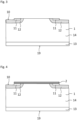
- Figure 1 shows a first position in an exemplary embodiment of the method for producing a semiconductor device.
- a semiconductor body 1 is provided with a top side 10 and a bottom side 19, opposite to the top side 10. At least the top side 10 is formed of SiC.
- the semiconductor body 1 may completely consist of SiC. Particularly, the semiconductor body 1 of figure 1 consists of n-doped semiconductor material.
- Figure 2 shows a position in which the top side 10 of the semiconductor body 1 is cleaned.
- the semiconductor body 1 has been further processed.
- p-doped base regions 12 have been formed inside the semiconductor body 1, e.g. with the help of ion implantation.
- n-doped contact regions 11 have been formed, e.g. also with the help of ion implantation.
- the n-doped contact regions 11 are separated and spaced from a drift region 14 of the semiconductor body 1 by the base regions 12.
- the drift region 14 is also n-doped.
- An n-doped contact layer 13 has been formed at the bottom side 19 of the semiconductor body 1.
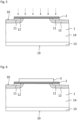
- Figure 6 shows a position after annealing of the dielectric layer 2 and after application of an electrically conductive layer 3 in the form of a gate electrode 3 onto the dielectric layer 2.
- the gate electrode 3 is, for example, formed of highly-doped polysilicon.
- the dielectric layer 2 forms the gate dielectric.
- Figures 9 and 10 show measurements of the capacitance voltage characteristics of different dielectric layers applied onto SiC epi wafers.
- the y-axis shows the relative capacitance C/Cmax and the x-axis shows the applied voltage Vg.
- the dielectric layer consists of a nitride, e.g. Si 3 N 4 .
- the curve A1 shows the result when the dielectric layer 2 is annealed in a pure nitrogen atmosphere and the curve A2 shows the result when the dielectric layer is annealed in an atmosphere comprising nitrogen and hydrogen, namely about 4 at-% of hydrogen.
- a stack of an oxide layer and a nitride-based dielectric layer is applied onto the wafer.
- Curve B1 shows the result of this stack being annealed in a pure nitrogen atmosphere
- curve B2 shows the result of the dielectric layer being annealed in an atmosphere comprising nitrogen and hydrogen.
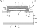
- FIG. 11 shows a further exemplary embodiment of the semiconductor device 100. It is similar to the one of figure 7 . However, in this case, the contact layer 13 is p-doped so that the semiconductor device 100 constitutes an IGBT.
Landscapes
- Formation Of Insulating Films (AREA)
- Electrodes Of Semiconductors (AREA)
Priority Applications (3)
| Application Number | Priority Date | Filing Date | Title |
|---|---|---|---|
| EP23192336.8A EP4513567B1 (fr) | 2023-08-21 | 2023-08-21 | Procédé de fabrication d'un dispositif semi-conducteur en carbure de silicium et dispositif semi-conducteur |
| CN202480054015.8A CN121729994A (zh) | 2023-08-21 | 2024-08-20 | 用于生产半导体设备的方法及半导体设备 |
| PCT/EP2024/073257 WO2025040646A1 (fr) | 2023-08-21 | 2024-08-20 | Procédé de production d'un dispositif à semi-conducteur et dispositif à semi-conducteur |
Applications Claiming Priority (1)
| Application Number | Priority Date | Filing Date | Title |
|---|---|---|---|
| EP23192336.8A EP4513567B1 (fr) | 2023-08-21 | 2023-08-21 | Procédé de fabrication d'un dispositif semi-conducteur en carbure de silicium et dispositif semi-conducteur |
Publications (2)
| Publication Number | Publication Date |
|---|---|
| EP4513567A1 true EP4513567A1 (fr) | 2025-02-26 |
| EP4513567B1 EP4513567B1 (fr) | 2025-08-13 |
Family
ID=87762776
Family Applications (1)
| Application Number | Title | Priority Date | Filing Date |
|---|---|---|---|
| EP23192336.8A Active EP4513567B1 (fr) | 2023-08-21 | 2023-08-21 | Procédé de fabrication d'un dispositif semi-conducteur en carbure de silicium et dispositif semi-conducteur |
Country Status (3)
| Country | Link |
|---|---|
| EP (1) | EP4513567B1 (fr) |
| CN (1) | CN121729994A (fr) |
| WO (1) | WO2025040646A1 (fr) |
Citations (5)
| Publication number | Priority date | Publication date | Assignee | Title |
|---|---|---|---|---|
| US20120223338A1 (en) * | 2009-09-07 | 2012-09-06 | Rohm Co. Ltd. | Semiconductor device and method of manufacturing the same |
| US20190267451A1 (en) * | 2018-02-28 | 2019-08-29 | Fuji Electric Co., Ltd. | Silicon carbide semiconductor device and method of manufacturing silicon carbide semiconductor device |
| US20190296146A1 (en) * | 2018-03-21 | 2019-09-26 | Kabushiki Kaisha Toshiba | Semiconductor device, method for manufacturing semiconductor device, inverter circuit, driving device, vehicle, and elevator |
| US20200091297A1 (en) * | 2018-09-14 | 2020-03-19 | Kabushiki Kaisha Toshiba | Semiconductor device, method for manufacturing semiconductor device, inverter circuit, driving device, vehicle, and elevator |
| US20200220001A1 (en) * | 2019-01-04 | 2020-07-09 | Kabushiki Kaisha Toshiba | Semiconductor device, inverter circuit, driving device, vehicle, and elevator |
Family Cites Families (2)
| Publication number | Priority date | Publication date | Assignee | Title |
|---|---|---|---|---|
| JP6692265B2 (ja) * | 2016-09-16 | 2020-05-13 | 株式会社東芝 | 半導体装置、半導体装置の製造方法、インバータ回路、駆動装置、車両、及び、昇降機 |
| WO2021185554A1 (fr) | 2020-03-17 | 2021-09-23 | Abb Power Grids Switzerland Ag | Structure de grille isolée, dispositif d'alimentation en matériau à large bande interdite doté de celle-ci et son procédé de fabrication |
-
2023
- 2023-08-21 EP EP23192336.8A patent/EP4513567B1/fr active Active
-
2024
- 2024-08-20 CN CN202480054015.8A patent/CN121729994A/zh active Pending
- 2024-08-20 WO PCT/EP2024/073257 patent/WO2025040646A1/fr active Pending
Patent Citations (5)
| Publication number | Priority date | Publication date | Assignee | Title |
|---|---|---|---|---|
| US20120223338A1 (en) * | 2009-09-07 | 2012-09-06 | Rohm Co. Ltd. | Semiconductor device and method of manufacturing the same |
| US20190267451A1 (en) * | 2018-02-28 | 2019-08-29 | Fuji Electric Co., Ltd. | Silicon carbide semiconductor device and method of manufacturing silicon carbide semiconductor device |
| US20190296146A1 (en) * | 2018-03-21 | 2019-09-26 | Kabushiki Kaisha Toshiba | Semiconductor device, method for manufacturing semiconductor device, inverter circuit, driving device, vehicle, and elevator |
| US20200091297A1 (en) * | 2018-09-14 | 2020-03-19 | Kabushiki Kaisha Toshiba | Semiconductor device, method for manufacturing semiconductor device, inverter circuit, driving device, vehicle, and elevator |
| US20200220001A1 (en) * | 2019-01-04 | 2020-07-09 | Kabushiki Kaisha Toshiba | Semiconductor device, inverter circuit, driving device, vehicle, and elevator |
Also Published As
| Publication number | Publication date |
|---|---|
| CN121729994A (zh) | 2026-03-24 |
| WO2025040646A1 (fr) | 2025-02-27 |
| EP4513567B1 (fr) | 2025-08-13 |
Similar Documents
| Publication | Publication Date | Title |
|---|---|---|
| US11777030B2 (en) | Semiconductor device | |
| US6841436B2 (en) | Method of fabricating SiC semiconductor device | |
| JP7241704B2 (ja) | 半導体装置およびその製造方法 | |
| EP1523032B1 (fr) | Procédé de fabrication d'une structure à couche en oxide de carbure de silicium | |
| US20070111423A1 (en) | Method of fabricating semiconductor device | |
| US20140103428A1 (en) | Trench superjunction mosfet with thin epi process | |
| US8564017B2 (en) | Silicon carbide semiconductor device and method for manufacturing same | |
| US8415241B2 (en) | Method of manufacturing silicon carbide semiconductor device | |
| JP4965576B2 (ja) | 半導体装置及びその製造方法 | |
| US8174076B2 (en) | Method for manufacturing electronic devices integrated in a semiconductor substrate and corresponding devices | |
| EP3931862B1 (fr) | Structure de grille isolée, dispositif de puissance utilisant un matériau à large bande interdite comprenant la structure et procédé de fabrication de la structure | |
| US6501135B1 (en) | Germanium-on-insulator (GOI) device | |
| EP4513567B1 (fr) | Procédé de fabrication d'un dispositif semi-conducteur en carbure de silicium et dispositif semi-conducteur | |
| US20250331263A1 (en) | SiC WAFER AND MANUFACTURING METHOD THEREOF | |
| US20230299192A1 (en) | Semiconductor device, semiconductor device manufacturing method, inverter circuit, drive device, vehicle, and elevator | |
| KR20080033351A (ko) | 반도체 장치의 제조 방법 |
Legal Events
| Date | Code | Title | Description |
|---|---|---|---|
| STAA | Information on the status of an ep patent application or granted ep patent |
Free format text: STATUS: EXAMINATION IS IN PROGRESS |
|
| PUAI | Public reference made under article 153(3) epc to a published international application that has entered the european phase |
Free format text: ORIGINAL CODE: 0009012 |
|
| REG | Reference to a national code |
Ref country code: DE Ref legal event code: R079 Ref country code: DE Ref legal event code: R079 Ref document number: 602023005655 Country of ref document: DE Free format text: PREVIOUS MAIN CLASS: H01L0029160000 Ipc: H10D0012000000 |
|
| 17P | Request for examination filed |
Effective date: 20240313 |
|
| AK | Designated contracting states |
Kind code of ref document: A1 Designated state(s): AL AT BE BG CH CY CZ DE DK EE ES FI FR GB GR HR HU IE IS IT LI LT LU LV MC ME MK MT NL NO PL PT RO RS SE SI SK SM TR |
|
| GRAP | Despatch of communication of intention to grant a patent |
Free format text: ORIGINAL CODE: EPIDOSNIGR1 |
|
| STAA | Information on the status of an ep patent application or granted ep patent |
Free format text: STATUS: GRANT OF PATENT IS INTENDED |
|
| RIC1 | Information provided on ipc code assigned before grant |
Ipc: H01L 21/04 20060101ALI20250225BHEP Ipc: H10D 12/01 20250101ALI20250225BHEP Ipc: H10D 64/68 20250101ALI20250225BHEP Ipc: H10D 62/832 20250101ALI20250225BHEP Ipc: H10D 30/66 20250101ALI20250225BHEP Ipc: H10D 12/00 20250101AFI20250225BHEP |
|
| INTG | Intention to grant announced |
Effective date: 20250311 |
|
| GRAS | Grant fee paid |
Free format text: ORIGINAL CODE: EPIDOSNIGR3 |
|
| GRAA | (expected) grant |
Free format text: ORIGINAL CODE: 0009210 |
|
| STAA | Information on the status of an ep patent application or granted ep patent |
Free format text: STATUS: THE PATENT HAS BEEN GRANTED |
|
| AK | Designated contracting states |
Kind code of ref document: B1 Designated state(s): AL AT BE BG CH CY CZ DE DK EE ES FI FR GB GR HR HU IE IS IT LI LT LU LV MC ME MK MT NL NO PL PT RO RS SE SI SK SM TR |
|
| REG | Reference to a national code |
Ref country code: GB Ref legal event code: FG4D |
|
| REG | Reference to a national code |
Ref country code: CH Ref legal event code: EP |
|
| REG | Reference to a national code |
Ref country code: DE Ref legal event code: R096 Ref document number: 602023005655 Country of ref document: DE |
|
| P01 | Opt-out of the competence of the unified patent court (upc) registered |
Free format text: CASE NUMBER: UPC_APP_2297_4513567/2025 Effective date: 20250804 |
|
| REG | Reference to a national code |
Ref country code: IE Ref legal event code: FG4D |
|
| PGFP | Annual fee paid to national office [announced via postgrant information from national office to epo] |
Ref country code: DE Payment date: 20250820 Year of fee payment: 3 |
|
| PGFP | Annual fee paid to national office [announced via postgrant information from national office to epo] |
Ref country code: AT Payment date: 20251020 Year of fee payment: 3 |
|
| REG | Reference to a national code |
Ref country code: NL Ref legal event code: MP Effective date: 20250813 |
|
| PG25 | Lapsed in a contracting state [announced via postgrant information from national office to epo] |
Ref country code: IS Free format text: LAPSE BECAUSE OF FAILURE TO SUBMIT A TRANSLATION OF THE DESCRIPTION OR TO PAY THE FEE WITHIN THE PRESCRIBED TIME-LIMIT Effective date: 20251213 |
|
| PG25 | Lapsed in a contracting state [announced via postgrant information from national office to epo] |
Ref country code: NO Free format text: LAPSE BECAUSE OF FAILURE TO SUBMIT A TRANSLATION OF THE DESCRIPTION OR TO PAY THE FEE WITHIN THE PRESCRIBED TIME-LIMIT Effective date: 20251113 |
|
| REG | Reference to a national code |
Ref country code: LT Ref legal event code: MG9D |
|
| PG25 | Lapsed in a contracting state [announced via postgrant information from national office to epo] |
Ref country code: PT Free format text: LAPSE BECAUSE OF FAILURE TO SUBMIT A TRANSLATION OF THE DESCRIPTION OR TO PAY THE FEE WITHIN THE PRESCRIBED TIME-LIMIT Effective date: 20251215 |
|
| PG25 | Lapsed in a contracting state [announced via postgrant information from national office to epo] |
Ref country code: FI Free format text: LAPSE BECAUSE OF FAILURE TO SUBMIT A TRANSLATION OF THE DESCRIPTION OR TO PAY THE FEE WITHIN THE PRESCRIBED TIME-LIMIT Effective date: 20250813 |
|
| PG25 | Lapsed in a contracting state [announced via postgrant information from national office to epo] |
Ref country code: HR Free format text: LAPSE BECAUSE OF FAILURE TO SUBMIT A TRANSLATION OF THE DESCRIPTION OR TO PAY THE FEE WITHIN THE PRESCRIBED TIME-LIMIT Effective date: 20250813 Ref country code: NL Free format text: LAPSE BECAUSE OF FAILURE TO SUBMIT A TRANSLATION OF THE DESCRIPTION OR TO PAY THE FEE WITHIN THE PRESCRIBED TIME-LIMIT Effective date: 20250813 |
|
| PG25 | Lapsed in a contracting state [announced via postgrant information from national office to epo] |
Ref country code: GR Free format text: LAPSE BECAUSE OF FAILURE TO SUBMIT A TRANSLATION OF THE DESCRIPTION OR TO PAY THE FEE WITHIN THE PRESCRIBED TIME-LIMIT Effective date: 20251114 |
|
| PG25 | Lapsed in a contracting state [announced via postgrant information from national office to epo] |
Ref country code: SE Free format text: LAPSE BECAUSE OF FAILURE TO SUBMIT A TRANSLATION OF THE DESCRIPTION OR TO PAY THE FEE WITHIN THE PRESCRIBED TIME-LIMIT Effective date: 20250813 |
|
| PG25 | Lapsed in a contracting state [announced via postgrant information from national office to epo] |
Ref country code: LV Free format text: LAPSE BECAUSE OF FAILURE TO SUBMIT A TRANSLATION OF THE DESCRIPTION OR TO PAY THE FEE WITHIN THE PRESCRIBED TIME-LIMIT Effective date: 20250813 |
|
| PG25 | Lapsed in a contracting state [announced via postgrant information from national office to epo] |
Ref country code: PL Free format text: LAPSE BECAUSE OF FAILURE TO SUBMIT A TRANSLATION OF THE DESCRIPTION OR TO PAY THE FEE WITHIN THE PRESCRIBED TIME-LIMIT Effective date: 20250813 Ref country code: BG Free format text: LAPSE BECAUSE OF FAILURE TO SUBMIT A TRANSLATION OF THE DESCRIPTION OR TO PAY THE FEE WITHIN THE PRESCRIBED TIME-LIMIT Effective date: 20250813 |
|
| PG25 | Lapsed in a contracting state [announced via postgrant information from national office to epo] |
Ref country code: RS Free format text: LAPSE BECAUSE OF FAILURE TO SUBMIT A TRANSLATION OF THE DESCRIPTION OR TO PAY THE FEE WITHIN THE PRESCRIBED TIME-LIMIT Effective date: 20251113 |
|
| PG25 | Lapsed in a contracting state [announced via postgrant information from national office to epo] |
Ref country code: ES Free format text: LAPSE BECAUSE OF FAILURE TO SUBMIT A TRANSLATION OF THE DESCRIPTION OR TO PAY THE FEE WITHIN THE PRESCRIBED TIME-LIMIT Effective date: 20250813 |
|
| REG | Reference to a national code |
Ref country code: AT Ref legal event code: MK05 Ref document number: 1826214 Country of ref document: AT Kind code of ref document: T Effective date: 20250813 |
|
| PG25 | Lapsed in a contracting state [announced via postgrant information from national office to epo] |
Ref country code: RO Free format text: LAPSE BECAUSE OF FAILURE TO SUBMIT A TRANSLATION OF THE DESCRIPTION OR TO PAY THE FEE WITHIN THE PRESCRIBED TIME-LIMIT Effective date: 20250813 |
|
| PG25 | Lapsed in a contracting state [announced via postgrant information from national office to epo] |
Ref country code: SM Free format text: LAPSE BECAUSE OF FAILURE TO SUBMIT A TRANSLATION OF THE DESCRIPTION OR TO PAY THE FEE WITHIN THE PRESCRIBED TIME-LIMIT Effective date: 20250813 |
|
| PG25 | Lapsed in a contracting state [announced via postgrant information from national office to epo] |
Ref country code: DK Free format text: LAPSE BECAUSE OF FAILURE TO SUBMIT A TRANSLATION OF THE DESCRIPTION OR TO PAY THE FEE WITHIN THE PRESCRIBED TIME-LIMIT Effective date: 20250813 |
|
| PG25 | Lapsed in a contracting state [announced via postgrant information from national office to epo] |
Ref country code: AT Free format text: LAPSE BECAUSE OF FAILURE TO SUBMIT A TRANSLATION OF THE DESCRIPTION OR TO PAY THE FEE WITHIN THE PRESCRIBED TIME-LIMIT Effective date: 20250813 |
|
| PG25 | Lapsed in a contracting state [announced via postgrant information from national office to epo] |
Ref country code: IT Free format text: LAPSE BECAUSE OF FAILURE TO SUBMIT A TRANSLATION OF THE DESCRIPTION OR TO PAY THE FEE WITHIN THE PRESCRIBED TIME-LIMIT Effective date: 20250813 Ref country code: LU Free format text: LAPSE BECAUSE OF NON-PAYMENT OF DUE FEES Effective date: 20250821 |
|
| PG25 | Lapsed in a contracting state [announced via postgrant information from national office to epo] |
Ref country code: CZ Free format text: LAPSE BECAUSE OF FAILURE TO SUBMIT A TRANSLATION OF THE DESCRIPTION OR TO PAY THE FEE WITHIN THE PRESCRIBED TIME-LIMIT Effective date: 20250813 |
|
| PG25 | Lapsed in a contracting state [announced via postgrant information from national office to epo] |
Ref country code: EE Free format text: LAPSE BECAUSE OF FAILURE TO SUBMIT A TRANSLATION OF THE DESCRIPTION OR TO PAY THE FEE WITHIN THE PRESCRIBED TIME-LIMIT Effective date: 20250813 Ref country code: SK Free format text: LAPSE BECAUSE OF FAILURE TO SUBMIT A TRANSLATION OF THE DESCRIPTION OR TO PAY THE FEE WITHIN THE PRESCRIBED TIME-LIMIT Effective date: 20250813 |