EP4528735A1 - Verbesserte sram-speicherinitialisierungsverwaltungsvorrichtung - Google Patents
Verbesserte sram-speicherinitialisierungsverwaltungsvorrichtung Download PDFInfo
- Publication number
- EP4528735A1 EP4528735A1 EP24199047.2A EP24199047A EP4528735A1 EP 4528735 A1 EP4528735 A1 EP 4528735A1 EP 24199047 A EP24199047 A EP 24199047A EP 4528735 A1 EP4528735 A1 EP 4528735A1
- Authority
- EP
- European Patent Office
- Prior art keywords
- initialization
- type
- control unit
- cells
- group
- Prior art date
- Legal status (The legal status is an assumption and is not a legal conclusion. Google has not performed a legal analysis and makes no representation as to the accuracy of the status listed.)
- Pending
Links
- 230000015654 memory Effects 0.000 title claims abstract description 105
- 230000000873 masking effect Effects 0.000 claims abstract description 90
- 210000004027 cell Anatomy 0.000 claims description 169
- 230000006870 function Effects 0.000 claims description 34
- 238000001514 detection method Methods 0.000 claims description 32
- 230000004913 activation Effects 0.000 claims description 18
- 230000008859 change Effects 0.000 claims description 17
- 230000003068 static effect Effects 0.000 claims description 9
- 230000000295 complement effect Effects 0.000 claims description 7
- 238000003860 storage Methods 0.000 claims description 4
- 238000013500 data storage Methods 0.000 claims description 2
- 210000000352 storage cell Anatomy 0.000 claims description 2
- 108010076504 Protein Sorting Signals Proteins 0.000 abstract description 3
- 235000021183 entrée Nutrition 0.000 description 17
- 230000000875 corresponding effect Effects 0.000 description 14
- 239000011159 matrix material Substances 0.000 description 9
- 238000000034 method Methods 0.000 description 9
- 230000000694 effects Effects 0.000 description 8
- 230000007704 transition Effects 0.000 description 5
- 238000004458 analytical method Methods 0.000 description 4
- 238000004519 manufacturing process Methods 0.000 description 4
- 230000001960 triggered effect Effects 0.000 description 4
- 238000010586 diagram Methods 0.000 description 3
- 241001080024 Telles Species 0.000 description 2
- 230000001276 controlling effect Effects 0.000 description 2
- 238000010304 firing Methods 0.000 description 2
- 238000007726 management method Methods 0.000 description 2
- 230000008569 process Effects 0.000 description 2
- 101100536354 Drosophila melanogaster tant gene Proteins 0.000 description 1
- 230000003213 activating effect Effects 0.000 description 1
- 239000000783 alginic acid Substances 0.000 description 1
- 235000010443 alginic acid Nutrition 0.000 description 1
- 230000005540 biological transmission Effects 0.000 description 1
- 239000000648 calcium alginate Substances 0.000 description 1
- 235000010410 calcium alginate Nutrition 0.000 description 1
- 230000002596 correlated effect Effects 0.000 description 1
- 238000007599 discharging Methods 0.000 description 1
- 230000007774 longterm Effects 0.000 description 1
- 230000007246 mechanism Effects 0.000 description 1
- 230000002093 peripheral effect Effects 0.000 description 1
- 230000000704 physical effect Effects 0.000 description 1
- 239000000737 potassium alginate Substances 0.000 description 1
- 235000010408 potassium alginate Nutrition 0.000 description 1
- 230000000750 progressive effect Effects 0.000 description 1
- 230000000630 rising effect Effects 0.000 description 1
- 238000012163 sequencing technique Methods 0.000 description 1
- 238000004513 sizing Methods 0.000 description 1
- 239000000661 sodium alginate Substances 0.000 description 1
- 235000010413 sodium alginate Nutrition 0.000 description 1
- 230000002123 temporal effect Effects 0.000 description 1
Images


Classifications
-
- G—PHYSICS
- G11—INFORMATION STORAGE
- G11C—STATIC STORES
- G11C11/00—Digital stores characterised by the use of particular electric or magnetic storage elements; Storage elements therefor
- G11C11/21—Digital stores characterised by the use of particular electric or magnetic storage elements; Storage elements therefor using electric elements
- G11C11/34—Digital stores characterised by the use of particular electric or magnetic storage elements; Storage elements therefor using electric elements using semiconductor devices
- G11C11/40—Digital stores characterised by the use of particular electric or magnetic storage elements; Storage elements therefor using electric elements using semiconductor devices using transistors
- G11C11/41—Digital stores characterised by the use of particular electric or magnetic storage elements; Storage elements therefor using electric elements using semiconductor devices using transistors forming static cells with positive feedback, i.e. cells not needing refreshing or charge regeneration, e.g. bistable multivibrator or Schmitt trigger
- G11C11/412—Digital stores characterised by the use of particular electric or magnetic storage elements; Storage elements therefor using electric elements using semiconductor devices using transistors forming static cells with positive feedback, i.e. cells not needing refreshing or charge regeneration, e.g. bistable multivibrator or Schmitt trigger using field-effect transistors only
-
- G—PHYSICS
- G11—INFORMATION STORAGE
- G11C—STATIC STORES
- G11C11/00—Digital stores characterised by the use of particular electric or magnetic storage elements; Storage elements therefor
- G11C11/21—Digital stores characterised by the use of particular electric or magnetic storage elements; Storage elements therefor using electric elements
- G11C11/34—Digital stores characterised by the use of particular electric or magnetic storage elements; Storage elements therefor using electric elements using semiconductor devices
- G11C11/40—Digital stores characterised by the use of particular electric or magnetic storage elements; Storage elements therefor using electric elements using semiconductor devices using transistors
- G11C11/41—Digital stores characterised by the use of particular electric or magnetic storage elements; Storage elements therefor using electric elements using semiconductor devices using transistors forming static cells with positive feedback, i.e. cells not needing refreshing or charge regeneration, e.g. bistable multivibrator or Schmitt trigger
- G11C11/413—Auxiliary circuits, e.g. for addressing, decoding, driving, writing, sensing, timing or power reduction
- G11C11/417—Auxiliary circuits, e.g. for addressing, decoding, driving, writing, sensing, timing or power reduction for memory cells of the field-effect type
-
- G—PHYSICS
- G11—INFORMATION STORAGE
- G11C—STATIC STORES
- G11C5/00—Details of stores covered by group G11C11/00
- G11C5/14—Power supply arrangements, e.g. power down, chip selection or deselection, layout of wirings or power grids, or multiple supply levels
- G11C5/148—Details of power up or power down circuits, standby circuits or recovery circuits
-
- G—PHYSICS
- G11—INFORMATION STORAGE
- G11C—STATIC STORES
- G11C7/00—Arrangements for writing information into, or reading information out from, a digital store
- G11C7/20—Memory cell initialisation circuits, e.g. when powering up or down, memory clear, latent image memory
-
- G—PHYSICS
- G11—INFORMATION STORAGE
- G11C—STATIC STORES
- G11C7/00—Arrangements for writing information into, or reading information out from, a digital store
- G11C7/24—Memory cell safety or protection circuits, e.g. arrangements for preventing inadvertent reading or writing; Status cells; Test cells
Definitions
- the present invention relates to the field of memories, and in particular of the SRAM type (SRAM for " Static Random Access Memory”), and more precisely concerns that of the initialization of SRAM memories.
- SRAM Static Random Access Memory
- the present invention implements an improved device making it possible to manage the selection of a type of initialization from among several possible types of initialization of a group of memory cells when this group of cells is powered up and of particular operating modes such as a secure operating mode or of particular events such as detection of fraudulent access to the memory.
- a known type of initialization is the so-called "free" initialization, which consists of an unconstrained firing of a plane of memory cells.
- free initialization the state in which each cell is initialized is established freely.
- the cell in the i -th column and j -th row has a probability p ijk of initializing to a logic level '1' and a probability 1-p ijk of initializing to a logic level '0'.
- the initialization state of the memory or of certain memory cells is thus likely to constitute a digital fingerprint or signature.
- the cells with a high probability of switching and initializing at a given logic level ( p ijk equal to or very close to 1 for cells with a strong tendency to initialize at '1'; and p ijk equal to or very close to 0 for cells with a strong tendency to initialize at '0') which can be used to form this digital fingerprint of the k -th chip.
- a disadvantage of free initialization may be that in case of malicious intrusion after such initialization, a third-party device may possibly recover this fingerprint or digital signature.
- Another initialization technique called “deterministic” consists of writing, address after address, a predetermined content which may have been previously fixed by the user or the designer of the memory.
- the "set to 0" type in which the state of each memory cell is forced to a logical value '0' or of the "set to 1" type in which the state of each memory cell is forced to a logical value '1' or of the "set to 1" type.
- the implementation of this type of initialization is done here at the expense of the time spent rewriting a certain number of memory points at different addresses, at the expense of the associated consumption as well as the risk of an information leak linked to this rewriting or carried out in a malicious way during this long operation.
- PMOS type transistors used in SRAM cells undergo a physical phenomenon called NBTI (in English “ Negative-Bias Temperature Instability » i.e. « Temperature instability in negative bias » ), which has the effect of increasing their threshold voltage, all the more so when their dimensions (length and width of gate) are reduced. This phenomenon is also accelerated when the temperature and/or the negative voltage VGS applied between the gate and the source of the transistor increase.
- An SRAM memory cell is commonly equipped with two inverters connected in a head-to-tail crossed manner, each being formed in particular of a first P-type transistor and a second N-type transistor.
- the value stored in an SRAM memory cell will influence the PMOS transistors of the same memory cell differently and the VTP1/VTP2 ratio of the respective threshold voltages of the two PMOS transistors will change over time in one direction or the other depending on the stored value.
- the NBTI phenomenon influences the probability of an SRAM cell to spontaneously initialize upon power-up to logic level '1' or its opposite level '0', since the initialization logic level is related to the VTP1/VTP2 ratio.
- memory data from the initialization of SRAM cells can be used to generate encryption keys or a hardware identifier or a unique digital fingerprint. They can be used to constitute a physical unclonable function (PUF).
- PEF physical unclonable function
- Some cells with a high VTP1/VTP2 ratio can be identified in particular as cells that are sufficiently stable to be used to form a PUF function during a so-called enrollment phase.
- the VTP1/VTP2 ratio may change over time, making the cells less suitable for use in forming a PUF, one of the prerequisites of which is long-term temporal stability.
- CPA power analysis
- DPA correlated power analysis
- Differential power analysis can be used to reveal data intended to remain secret, based among other things on this phenomenon of drift in the threshold voltage of transistors by using means to accelerate this drift.
- Such a technique is described for example in the document: “ Power Analysis: Resilient SRAM Design Implemented with a 1% Area Overhead Impedance Randomization Unit for Security Applications", by R. Giterman et al., ESSCIRC 2019 .
- the detection signal may come from a module for detecting fraudulent access to said SRAM memory, said locking sequence on said first hard masking input corresponding to a change of state of said detection signal.
- the unlocking sequence may consist, in this order, of a given logic state or a change of logic state of said detection signal on said first hard masking input to said logic state given then, a change of the activation signal on said second hard masking input.
- maintaining the output of said control signal in the same given state is capable of maintaining said given group of cells in an indeterminate state called “metastable” for which their respective first storage node and their second storage node are set to equal or substantially equal potentials.
- the given group of cells may contain a physical unclonable function (PUF), while the second group of cells corresponding to sensitive data storage cells or open access cells.
- PEF physical unclonable function
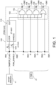
- This control unit 100 is capable of triggering different distinct initialization types and makes it possible to trigger an initialization of said at least one given group of cells according to an initialization type selected from different distinct initialization types.
- a third soft masking input SM3 may also be provided for receiving a logic signal R indicating a third type of initialization, here corresponding to a so-called “random” initialization (and which may also be called “random deterministic” or “random by column”) of memory cells.
- a fourth soft masking input SM4 is also provided for receiving a logic signal O indicating a fourth type of initialization in this example of the “setting to 1” type of the memory cells.
- the control unit 100 is here formed of an asynchronous flip-flop logic module 110 having a LOCK input coupled to the first hard masking input HM1 and another HANDLE input coupled to the second hard masking input HM2.
- This logic module 110 produces at output a logic output signal OUT whose state is transmitted to a logic stage 150.
- the inputs of the module 110 are, in this example, directly connected respectively to the hard masking inputs HM1, HM2.
- This initialization circuit (not shown in this figure) is itself configured to initialize said at least one given group of memory cells, according to different distinct initialization types depending on the initialization control signals F', R', O', Z' received.
- An initialization circuit of the type described in application No. 2111286, in particular in connection with its Figure 4 can be triggered by the Z' signal in order to allow all memory cells to be written to “0” and thus implement a “set to 0” type initialization.
- a second initialization control signal F' of another initialization type than the control signal Z', is likely to be produced on a second output OM2 of the control unit 100 and in particular by means of a logic gate 152 of the stage 150.
- This gate 152 performs in this example a logic function different from that of the gate 158, here an AND function, between the second soft masking input SM2 and the output OUT of the module 110.
- the initialization control signal F' is here provided to trigger an initialization of said group of cells according to an initialization of the "free" type.
- a third initialization control signal R' in this example of the "random" type of cells, is likely to be produced on a third output OM3 of the control unit 100 by a logic gate 154 of the stage 150 here performing an AND function, between the soft masking input SM3 and the output OUT of the module 110.
- the third initialization control signal is here provided to trigger an initialization of said group of cells according to an initialization of the "random" type.
- a fourth initialization control signal O' in this example of the "setting to '1'" type of the cells, is likely to be produced on a fourth output OM4 of the control unit 100 by a logic gate 156 of the stage 150 here performing an AND function, between the soft masking input SM4 and the output OUT of the module 110.
- the fourth initialization control signal is here provided to trigger an initialization of said group of cells according to an initialization of the "setting to '1'" type.
- An initialization circuit described in application No. 2111286, in particular in connection with its Figure 4 allows all memory cells to be written to "1" and thus implement a "set to 1" type initialization. To do this, the memory device plans to drive, for each column, one of the BLT or BLF bit lines by connecting it to a supply voltage by turning on a bit line selection transistor. The selected and powered bit line thus tends to impose a value "1” or "0" on one of the nodes of each memory cell connected to this bit line.
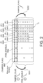
- the initialization control unit 100 is configured to adopt a so-called "locked" operating mode (first line of the truth table) in which the initialization control unit 10 is configured so that following a power-up, regardless of the value of signals emitted on the first hard mask input HM1, on the second hard masking input HM2 and on the soft masking inputs SM1, SM2, SM3, SM4, the control unit produces at output a control signal making it possible to trigger an initialization of said given group of cells according to a so-called "default” initialization type or an erasure of said given group of cells prior to placing this given group of cells in a metastable state.
- the given state of the signal Z' emitted on the first output OM1 is likely to cause erasure of the data and the placing of said at least one group of cells in a so-called "metastable" state for which their first node and second node are placed at equal or substantially equal potentials, in particular when the given group of cells associated with the control unit 100 are intended to perform a non-clonable physical function (PUF).
- PEF non-clonable physical function
- the internal nodes of the memory cells can be positioned at identical or substantially identical values (i.e. which differ by minus 10 mV), either by short circuit or by discharging the nodes following a power cut.
- a possible initialization phase therefore consists of switching a memory cell from an “indeterminate” state (and indeterminable by reading) to a state with a “determined” stored value (and therefore determinable by reading).
- the signal Z' emitted on the first output OM1 is likely to cause an initialization of this given group according to the type of initialization called “by default”.
- the type default initialization corresponds to the first type of initialization, in other words to an initialization of the "set to 0" type of cells.
- the control signal Z' can thus be used to trigger an initialization of the cells by "set to 0".
- This signal Z' on the output OM1 (here corresponding to a logic state 1) allows here, following a power-up of the memory, to trigger a reset to 0 of the cells of a group of cells associated with the control unit 100.
- set to 0 of the cells, we mean here a setting to a potential of their first node or their second node corresponding to a logic '0' according to which of these complementary nodes is supposed by convention to establish the logic state of the cell.
- a particular sequence of hard masking signals on the HM1 and HM2 inputs allows exit from the “default” operating mode.
- the unlocking sequence can advantageously correspond to a succession of signals on the first hard masking input HM1 then on the second hard masking input HM2.
- an unlocking sequence S201 consists of applying a given logic state, for example a logic '0' on the first hard masking input, then applying a falling edge (i.e. a transition from a logic '1' to a logic '0') on the second hard masking input.
- the logic module 110 After receiving such a sequence, the logic module 110 is no longer in its locked state and its output is no longer necessarily in the logic state '0' and is thus likely to be modified.
- a "soft masking" operating mode can then be established as long as new signals or a change in signal state on the hard masking inputs HM1, HM2 is not detected, which in this example results in a state being maintained, in particular a low state or a logic level '0', on the inputs HM1, HM2, it being the soft masking signals which control the initialization.
- control unit 100 when the control unit 100 receives a “set to 0” initialization indicator signal Z on its SM1 input (third line of the truth table), the control unit 100 produces at output a signal Z' initialization command of the "set to 0" type to trigger an initialization of the memory cells by setting these cells to a logic state '0'.
- the control unit 100 when the control unit receives a free-type initialization indicator signal F on its input SM2 (sixth line of the truth table), the control unit 100 produces as output a free-type initialization control signal F' to trigger a "free" type initialization of the memory cells.
- control unit 100 When the control unit 100 receives a random initialization indicator signal R' on its input SM3 (fifth line of the truth table), it produces at output an initialization control signal R' of the “random” type to trigger a random initialization of the memory cells.
- the control unit 100 When the initialization management unit receives an initialization indicator signal O of the “set to 1” type on its input SM4 (fourth line of the truth table), the control unit 100 produces at output an initialization control signal O' of the “set to 1” type to trigger a random initialization of the memory cells by setting these cells to a logic state '1'.
- the control unit when a given soft masking input SM1, SM2, SM3, SM4, receives an initialization indicator signal of a given initialization type, the control unit produces an initialization control signal at output to trigger an initialization of the memory cells of the given sector according to said given initialization type.
- the initialization control unit 100 is configured to re-adopt the so-called "default" operating mode following receipt of a locking signal or indicator on said first hard masking input HM1.
- Such a signal or indicator causes a locking S202 of the output OUT of the module 110.
- This locking is implemented by detecting a new sequence S202, for example when a rising edge (transition from a logic '0' to a logic '1') on the intrusion detection signal TAMPER_FLAG is detected. Following such detection, the control unit 100 operates again in its default mode in which, regardless of the value of the hard masking and soft masking inputs, a "default" initialization control logic signal is produced, in this example in the form of an initialization control signal of the "set to 0" type produced at output OM4 of the control unit 100.
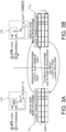
- FIG. 3 different operating modes of the logic module 110 are illustrated by means of a first truth table T 31 and a second truth table T 32 .
- step E400 corresponding here to a setting to VDD of a power supply rail of the module 110
- the module 100 is then (truth table T 31 ) in the “locked” operating mode of the control unit 100 and in which its output OUT always remains in the same logical state, here at '0'.
- the particular unlocking sequence (steps E401 then E402) to take the module 110 out of its “locked” state consists, for example, of applying a 0 to the LOCK input before applying a falling edge to the HANDLE input.
- the output signal OUT of the module 110 changes from the “locked” state when the power supply starts, in this example '0', to another state, in this example to '1'. This allows you to exit the default operating mode of the control unit described above.
- the output OUT can return to a logic state '0' allowing a “default” type initialization to be triggered (i.e. in the embodiment described previously corresponding to a “set to 0” type initialization) without putting the module 110 back into a locked state. This is achieved by setting the signal on the HANDLE input to '1'.
- step E404 the signal on the LOCK input is set to 1.
- This setting of the LOCK input to a logic state '1' may correspond to an activation or a setting of the "Tamper_Flag" signal to a logic state '1' following detection of a drop in supply voltage. Such detection is implemented, for example, by an external module or circuit for detecting fraudulent access.
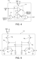
- FIG. 4 serves to illustrate a detailed embodiment of the logic module 110 mentioned above and receiving the hard masking signals from the hard masking inputs HM1, HM2, respectively on a first control input LOCK and a second control input HANDLE.
- the logic module 110 here integrates an asynchronous flip-flop 115, in particular an RS flip-flop, the R input of which is coupled to the first control input LOCK.
- the output of a logic gate 113 performing a logic function between the first control input LOCK and the second control input HANDLE is applied to the S input of the flip-flop.
- the logic gate 113 performs a NOR function between the first control input LOCK and the complement of the second control input HANDLE.
- the Q output of the flip-flop 115 is coupled to a logic gate 117 performing for example a NOR function and delivering the output signal OUT of module 110.
- the asynchronous flip-flop 115 has the particularity of being asymmetrical, so that when it is powered up (shown schematically on the Figure 4 by a passage from ground to a potential VDD of its power supply) it always initializes to the same logic state, here for example a logic state '1' on output Q.
- the RS type asynchronous flip-flop 115 can be made asymmetrical by asymmetrically sizing the two NOR or NAND gates that make up this flip-flop 115. Thus, by design, the initialization value of the module 110 is determined when it is powered.
- the flip-flop 115 is formed of a first set of transistors M1, M2, M5, M6 performing here a NOR logic function and a second set of transistors M3, M4, M7, M8 performing the same logic function as the first set of transistors M1, M2, M5, M6.
- the first set of transistors comprises a first group of transistors M1, M2, in this example N-type transistors, having an arrangement similar to that of a second group of transistors M3, M4, of N-type but provided with a lower threshold voltage than that of the transistors M3, M4 of the second group.
- the first set of transistors may be provided with a group of transistors M5, M6, in this example P-type transistors, having a similar arrangement to that of another group of transistors M7, M8, of P-type but provided with a threshold voltage greater than that of the transistors M7, M8.
- the asymmetry may also be obtained with different geometries of the transistors relative to each other and in particular their ratio (W/L) of width W to length L of the channel.
- FIG. 6 another initialization control unit 200 for controlling the initialization of at least one other given group of SRAM cells of the same SRAM memory as that provided with the group of cells controlled by the initialization control unit 100 is illustrated.
- This other initialization control unit 200 has a structure similar to that of the control unit 100 but differs in particular from that described in connection with the Figure 1 , in that its default initialization type this time corresponds to a “random” type initialization.
- the random initialization control signal R' therefore corresponds, in this example, to the default initialization control signal. This signal R' is emitted on the OM1 output.
- the initialization indicator signals O, F, R, Z are this time emitted respectively on the inputs SM3, SM2, SM1, SM4, while the initialization control signals O', F', R', Z' come this time respectively from the outputs OM3, OM2, OM1, OM4.
- control unit 100 and the other control unit 200 can be dedicated to managing the initialization of groups of cells belonging to different zones of a matrix or a memory plane.
- FIG. 7 An example of a memory map is shown schematically in the Figure 7 and comprises a matrix M of memory cells.
- the matrix is typically formed from a plurality of rows and columns of SRAM cells (not shown in this figure).
- two zones Z1, Z2 are distinguished in the matrix M, each formed from a group of cells.
- the memory comprises in particular a first group G1 of cells located in a first zone Z1 of the matrix.
- the first zone Z1 contains cells intended to perform a non-clonable physical function (PUF) and whose logical state, in particular the logical state initialization, is likely to be used to form a digital signature or a digital fingerprint of the memory.
- PAF non-clonable physical function
- the memory also comprises a second group G2 located in a second zone Z2 of the matrix typically larger in size than the first zone Z1.
- the second group G2 can be formed of several subgroups G21, G22 and advantageously comprise a subgroup G22 of cells capable of storing sensitive CSP data (for “Critical Security Parameters”).
- the memory can then have an initialization control unit 100 as described for example in connection with the Figure 1 dedicated to the first zone Z1 corresponding to the non-clonable physical function (PUF).
- Another control unit 200 as described for example in connection with the Figure 6 can be dedicated to the second zone Z2 and intended to control the initialization of the G22 subgroup of CSP cells that can store sensitive data. We can thus manage the default initialization and the sequencing of the initialization of the Z1 zone dedicated to the PUF differently from those of other zones and in particular of the CSP cell zone.
- the initialization control units 100, 200 may be implemented in a region peripheral to the memory cells, for example a region in which a row or column controller of the matrix is located.
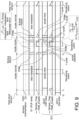
- timing diagram 9 gives an example of a timing diagram of the operation of a memory device which may be provided with one or more initialization control units as described above.
- the time scale on this timing diagram is not represented linearly, the ratio of the durations respectively between the times t1 and t2 and between the times t2 and 3 being typically much greater than on this schematic representation.
- Powering up the memory array here results in a transition from 0 to VDD of a grid or conductive line between a time t0 and a time t1.
- the cells of the first group G1 are then erased and then maintained in a metastable state while the cells of the subgroup G22 are initialized.
- the cells of the subgroup G22 will be initialized according to the default initialization type provided for powering up. Thus, for example, we can predict that the cells of the set G22 will have a random initialization.
- their high supply line VDD ( figure 8 ) is disconnected from a grid or power supply conductive line and/or their internal nodes N T and N F are connected to each other, for example by activating their access transistors TA T and TA F and connecting the bit lines BLTi, ..., BLFi together.
- a falling edge on the PDM_ENABLE activation signal puts the control unit associated with subgroup G22 of the CSP zone into an unlocked state, while the control unit associated with the first group G1 remains in a locked state.
- the device is in a so-called “normal” operating mode, which corresponds to a majority of the overall operating time of the matrix when it is powered, for example at least 99% and in this example 99.9% of the time when the power supply conductive grid is powered and thus set to the supply voltage VDD.
- the output(s) of the control unit associated with the first group G1 is not modified.
- This operating mode may in particular be an operating mode in which one wishes to access the cells of the first group G1 in order to carry out an enrollment procedure to determine the cells that one wishes to use to create a digital signature and/or an encryption key (PUF), or in order to read a digital signature and/or an encryption key contained in certain cells of the first group G1.
- PDM_ENABLE the state of the activation signal PDM_ENABLE is such that it does not modify not that of the output(s) of the control unit associated with the first group G1 of cells.
- a falling edge on the PDM_ENABLE activation signal unlocks the control unit associated with the first group G1 of cells.
- initializations according to initialization types that may be distinct from the default initialization type can be launched.
- "free” type initializations can be carried out during this phase on the cells of the first group G1.
- the CSP area is in a restricted access mode.
- control unit of the PUF zone being able to be distinct from the control unit of the CSP zone.
- a fraudulent access attempt to the memory may possibly be detected and results in a change of state of the Tamper_flag detection signal which, for example by means of a transition to a given state, here a high state corresponding to a logic '1', makes it possible to launch a default initialization of the cells of the first group G1 and the cells of the subgroup G22.
- the control unit(s) associated with the first group G1 and the subgroup G22 of cells are then put into a locked state.
- the cells of the first group G1 and the cells of the subgroup G22 are then put into a metastable state.
- An unlocking sequence (change of state of the detection signal then of the activation signal) then makes it possible to return the control unit associated with the first group G1 to an unlocked state, which again makes it possible to carry out one or more initializations on the cells of the first group G1 according to respective types which may be distinct from that of the default initialization.
- a new change of state of the activation signal can, from a time t3, make it possible to return to a “normal” operating mode.
- This change of state can occur in particular at the end of an enrollment operation or at the end of an “interrogation” or “challenge” operation of the PUF zone in which the cells of the first group G1 can be located.
- the first logic signal TAMPER_FLAG called "detection" described above and emitted at the input of the initialization control unit 100 may come from a module other than the fraudulent access detection module 11 mentioned above.
- a microprocessor or a microcontroller, or a logic circuit external to the memory circuit transmits to the initialization control unit 100 the first logic signal TAMPER_FLAG as a preventative measure, for example to protect a memory area or reserve privileged access to a memory area.
- the transmission of such a protection signal may possibly be carried out even before use of the memory, for example after its manufacture and during a factory test conducted by an operator.
- This operator having administration rights over the memory, triggers the emission of the logical signal TAMPER_FLAG by the aforementioned external module, in order to generate a sequence allowing, for example, the locking of a particular memory zone, for example of the ROM type and/or containing a secret code.
Landscapes
- Engineering & Computer Science (AREA)
- Microelectronics & Electronic Packaging (AREA)
- Computer Hardware Design (AREA)
- Power Engineering (AREA)
- Storage Device Security (AREA)
- Static Random-Access Memory (AREA)
Applications Claiming Priority (1)
| Application Number | Priority Date | Filing Date | Title |
|---|---|---|---|
| FR2309897A FR3153183B1 (fr) | 2023-09-19 | 2023-09-19 | Dispositif ameliore de gestion d’initialisation de memoire sram |
Publications (1)
| Publication Number | Publication Date |
|---|---|
| EP4528735A1 true EP4528735A1 (de) | 2025-03-26 |
Family
ID=90458036
Family Applications (1)
| Application Number | Title | Priority Date | Filing Date |
|---|---|---|---|
| EP24199047.2A Pending EP4528735A1 (de) | 2023-09-19 | 2024-09-06 | Verbesserte sram-speicherinitialisierungsverwaltungsvorrichtung |
Country Status (3)
| Country | Link |
|---|---|
| US (1) | US20250095723A1 (de) |
| EP (1) | EP4528735A1 (de) |
| FR (1) | FR3153183B1 (de) |
Citations (5)
| Publication number | Priority date | Publication date | Assignee | Title |
|---|---|---|---|---|
| FR2111286A5 (de) | 1970-10-15 | 1972-06-02 | Unitecta Oberflaechenschutz | |
| FR2213917A1 (de) | 1973-01-13 | 1974-08-09 | Delog Detag Flachglas Ag | |
| FR2214117A1 (de) | 1973-01-12 | 1974-08-09 | Bizerba Werke Kraut Kg Wilh | |
| JP2004335009A (ja) * | 2003-05-09 | 2004-11-25 | Nec Micro Systems Ltd | 半導体メモリ装置 |
| EP4170655A1 (de) * | 2021-10-25 | 2023-04-26 | Commissariat à l'énergie atomique et aux énergies alternatives | Sram mit rekonfigurierbarer initialisierung |
-
2023
- 2023-09-19 FR FR2309897A patent/FR3153183B1/fr active Active
-
2024
- 2024-09-06 EP EP24199047.2A patent/EP4528735A1/de active Pending
- 2024-09-12 US US18/882,959 patent/US20250095723A1/en active Pending
Patent Citations (5)
| Publication number | Priority date | Publication date | Assignee | Title |
|---|---|---|---|---|
| FR2111286A5 (de) | 1970-10-15 | 1972-06-02 | Unitecta Oberflaechenschutz | |
| FR2214117A1 (de) | 1973-01-12 | 1974-08-09 | Bizerba Werke Kraut Kg Wilh | |
| FR2213917A1 (de) | 1973-01-13 | 1974-08-09 | Delog Detag Flachglas Ag | |
| JP2004335009A (ja) * | 2003-05-09 | 2004-11-25 | Nec Micro Systems Ltd | 半導体メモリ装置 |
| EP4170655A1 (de) * | 2021-10-25 | 2023-04-26 | Commissariat à l'énergie atomique et aux énergies alternatives | Sram mit rekonfigurierbarer initialisierung |
Non-Patent Citations (2)
| Title |
|---|
| J. MCMAHAN ET AL.: "Challenging On-Chip SRAM Security with Boot-State Statistics", HOST, 2017 |
| R. GITERMAN ET AL.: "Power Analysis Resilient SRAM Design Implemented with a 1% Area Overhead Impedance Randomization Unit for Security Applications", ESSCIRC, 2019 |
Also Published As
| Publication number | Publication date |
|---|---|
| FR3153183B1 (fr) | 2025-09-19 |
| FR3153183A1 (fr) | 2025-03-21 |
| US20250095723A1 (en) | 2025-03-20 |
Similar Documents
| Publication | Publication Date | Title |
|---|---|---|
| EP3454320B1 (de) | Zufallscodegenerator und zugehöriges zufallscodeerzeugungsverfahren | |
| EP2842229B1 (de) | Reprogrammierbare logische vorrichtung mit strahlenwiderstandsfähigkeit | |
| US20180191512A1 (en) | Physically unclonable function generation with direct twin cell activation | |
| US20180287793A1 (en) | Random number generation with unstable bit states of non-volatile memory | |
| US10073989B2 (en) | Systems and methods for preventing data remanence in memory systems | |
| FR2715782A1 (fr) | Bascule bistable non volatile programmable, à état initial prédéfini, notamment pour circuit de redondance de mémoire. | |
| FR3128570A1 (fr) | Sram a initialisation reconfigurable | |
| EP3886361A1 (de) | Physisch nicht klonbares funktionsgerät | |
| EP3633677A1 (de) | Imc-speicherschaltkreis mit 6t-zellen | |
| EP3496101A1 (de) | Sram-speicher mit schneller löschfunktion | |
| WO2022207999A1 (fr) | Dispositif memoire et procede de protection d'un dispositif memoire de l'effet de martelage d'un rang | |
| EP3373303A1 (de) | Tfet-speicherlatch ohne aktualisierung | |
| EP4528735A1 (de) | Verbesserte sram-speicherinitialisierungsverwaltungsvorrichtung | |
| EP4390930A1 (de) | Sram mit puf-different-sektor-aufrechterhaltung | |
| EP3080813B1 (de) | System zur verwaltung des verschleisses eines elektronischen speichers | |
| US10970046B2 (en) | Random number generator compatible with complementary metal-oxide semiconductor technology | |
| FR3007185A1 (fr) | Dispositif de memoire associant un plan-memoire du type sram et un plan-memoire du type non volatil, et procedes de fonctionnement | |
| EP4390929A1 (de) | Sram-speicher mit deterministischer zufallsinitialisierung | |
| Noel et al. | A near-instantaneous and non-invasive erasure design technique to protect sensitive data stored in secure SRAMs | |
| EP3680904A1 (de) | Detektionsschaltkreis eines vorherrschenden dateninhalts in einer speicherzelle | |
| Chuang et al. | Highly reliable physically unclonable functions: Design, characterization and security analysis | |
| EP4539390A1 (de) | Kryptographische schlüsselerzeugung aus einem sram-speicher | |
| Okumura et al. | A 128-bit chip identification generating scheme exploiting load transistors' variation in SRAM bitcells | |
| Singh et al. | Memristor-Assisted Secure SRAM Architectures for Protection Against Data Imprinting Attacks | |
| Moka | A Physical-Unclonable-Function Circuit based on Cells Composed of Diode-Connected Transistors |
Legal Events
| Date | Code | Title | Description |
|---|---|---|---|
| PUAI | Public reference made under article 153(3) epc to a published international application that has entered the european phase |
Free format text: ORIGINAL CODE: 0009012 |
|
| STAA | Information on the status of an ep patent application or granted ep patent |
Free format text: STATUS: REQUEST FOR EXAMINATION WAS MADE |
|
| 17P | Request for examination filed |
Effective date: 20240906 |
|
| AK | Designated contracting states |
Kind code of ref document: A1 Designated state(s): AL AT BE BG CH CY CZ DE DK EE ES FI FR GB GR HR HU IE IS IT LI LT LU LV MC ME MK MT NL NO PL PT RO RS SE SI SK SM TR |