EP4529366A1 - Electrical connector for a data cable - Google Patents
Electrical connector for a data cable Download PDFInfo
- Publication number
- EP4529366A1 EP4529366A1 EP24189851.9A EP24189851A EP4529366A1 EP 4529366 A1 EP4529366 A1 EP 4529366A1 EP 24189851 A EP24189851 A EP 24189851A EP 4529366 A1 EP4529366 A1 EP 4529366A1
- Authority
- EP
- European Patent Office
- Prior art keywords
- circuit board
- electrical connector
- printed circuit
- conductive
- conductive surfaces
- Prior art date
- Legal status (The legal status is an assumption and is not a legal conclusion. Google has not performed a legal analysis and makes no representation as to the accuracy of the status listed.)
- Pending
Links
Images



Classifications
-
- H—ELECTRICITY
- H05—ELECTRIC TECHNIQUES NOT OTHERWISE PROVIDED FOR
- H05K—PRINTED CIRCUITS; CASINGS OR CONSTRUCTIONAL DETAILS OF ELECTRIC APPARATUS; MANUFACTURE OF ASSEMBLAGES OF ELECTRICAL COMPONENTS
- H05K1/00—Printed circuits
- H05K1/02—Details
- H05K1/0213—Electrical arrangements not otherwise provided for
- H05K1/0216—Reduction of cross-talk, noise or electromagnetic interference
-
- H—ELECTRICITY
- H01—ELECTRIC ELEMENTS
- H01R—ELECTRICALLY-CONDUCTIVE CONNECTIONS; STRUCTURAL ASSOCIATIONS OF A PLURALITY OF MUTUALLY-INSULATED ELECTRICAL CONNECTING ELEMENTS; COUPLING DEVICES; CURRENT COLLECTORS
- H01R13/00—Details of coupling devices of the kinds covered by groups H01R12/70 or H01R24/00 - H01R33/00
- H01R13/66—Structural association with built-in electrical component
- H01R13/665—Structural association with built-in electrical component with built-in electronic circuit
- H01R13/6658—Structural association with built-in electrical component with built-in electronic circuit on printed circuit board
-
- H—ELECTRICITY
- H01—ELECTRIC ELEMENTS
- H01R—ELECTRICALLY-CONDUCTIVE CONNECTIONS; STRUCTURAL ASSOCIATIONS OF A PLURALITY OF MUTUALLY-INSULATED ELECTRICAL CONNECTING ELEMENTS; COUPLING DEVICES; CURRENT COLLECTORS
- H01R24/00—Two-part coupling devices, or either of their cooperating parts, characterised by their overall structure
- H01R24/60—Contacts spaced along planar side wall transverse to longitudinal axis of engagement
- H01R24/62—Sliding engagements with one side only, e.g. modular jack coupling devices
- H01R24/64—Sliding engagements with one side only, e.g. modular jack coupling devices for high frequency, e.g. RJ 45
-
- H—ELECTRICITY
- H05—ELECTRIC TECHNIQUES NOT OTHERWISE PROVIDED FOR
- H05K—PRINTED CIRCUITS; CASINGS OR CONSTRUCTIONAL DETAILS OF ELECTRIC APPARATUS; MANUFACTURE OF ASSEMBLAGES OF ELECTRICAL COMPONENTS
- H05K1/00—Printed circuits
- H05K1/02—Details
- H05K1/0213—Electrical arrangements not otherwise provided for
- H05K1/0237—High frequency adaptations
- H05K1/025—Impedance arrangements, e.g. impedance matching, reduction of parasitic impedance
-
- H—ELECTRICITY
- H05—ELECTRIC TECHNIQUES NOT OTHERWISE PROVIDED FOR
- H05K—PRINTED CIRCUITS; CASINGS OR CONSTRUCTIONAL DETAILS OF ELECTRIC APPARATUS; MANUFACTURE OF ASSEMBLAGES OF ELECTRICAL COMPONENTS
- H05K1/00—Printed circuits
- H05K1/16—Printed circuits incorporating printed electric components, e.g. printed resistors, capacitors or inductors
- H05K1/162—Printed circuits incorporating printed electric components, e.g. printed resistors, capacitors or inductors incorporating printed capacitors
-
- H—ELECTRICITY
- H05—ELECTRIC TECHNIQUES NOT OTHERWISE PROVIDED FOR
- H05K—PRINTED CIRCUITS; CASINGS OR CONSTRUCTIONAL DETAILS OF ELECTRIC APPARATUS; MANUFACTURE OF ASSEMBLAGES OF ELECTRICAL COMPONENTS
- H05K2201/00—Indexing scheme relating to printed circuits covered by H05K1/00
- H05K2201/07—Electric details
- H05K2201/0776—Resistance and impedance
- H05K2201/0792—Means against parasitic impedance; Means against eddy currents
-
- H—ELECTRICITY
- H05—ELECTRIC TECHNIQUES NOT OTHERWISE PROVIDED FOR
- H05K—PRINTED CIRCUITS; CASINGS OR CONSTRUCTIONAL DETAILS OF ELECTRIC APPARATUS; MANUFACTURE OF ASSEMBLAGES OF ELECTRICAL COMPONENTS
- H05K2201/00—Indexing scheme relating to printed circuits covered by H05K1/00
- H05K2201/09—Shape and layout
- H05K2201/09209—Shape and layout details of conductors
- H05K2201/09654—Shape and layout details of conductors covering at least two types of conductors provided for in H05K2201/09218 - H05K2201/095
- H05K2201/09672—Superposed layout, i.e. in different planes
-
- H—ELECTRICITY
- H05—ELECTRIC TECHNIQUES NOT OTHERWISE PROVIDED FOR
- H05K—PRINTED CIRCUITS; CASINGS OR CONSTRUCTIONAL DETAILS OF ELECTRIC APPARATUS; MANUFACTURE OF ASSEMBLAGES OF ELECTRICAL COMPONENTS
- H05K2201/00—Indexing scheme relating to printed circuits covered by H05K1/00
- H05K2201/09—Shape and layout
- H05K2201/09209—Shape and layout details of conductors
- H05K2201/09654—Shape and layout details of conductors covering at least two types of conductors provided for in H05K2201/09218 - H05K2201/095
- H05K2201/09781—Dummy conductors, i.e. not used for normal transport of current; Dummy electrodes of components
-
- H—ELECTRICITY
- H05—ELECTRIC TECHNIQUES NOT OTHERWISE PROVIDED FOR
- H05K—PRINTED CIRCUITS; CASINGS OR CONSTRUCTIONAL DETAILS OF ELECTRIC APPARATUS; MANUFACTURE OF ASSEMBLAGES OF ELECTRICAL COMPONENTS
- H05K2201/00—Indexing scheme relating to printed circuits covered by H05K1/00
- H05K2201/10—Details of components or other objects attached to or integrated in a printed circuit board
- H05K2201/10227—Other objects, e.g. metallic pieces
- H05K2201/1028—Thin metal strips as connectors or conductors
-
- H—ELECTRICITY
- H05—ELECTRIC TECHNIQUES NOT OTHERWISE PROVIDED FOR
- H05K—PRINTED CIRCUITS; CASINGS OR CONSTRUCTIONAL DETAILS OF ELECTRIC APPARATUS; MANUFACTURE OF ASSEMBLAGES OF ELECTRICAL COMPONENTS
- H05K2201/00—Indexing scheme relating to printed circuits covered by H05K1/00
- H05K2201/10—Details of components or other objects attached to or integrated in a printed circuit board
- H05K2201/10227—Other objects, e.g. metallic pieces
- H05K2201/10333—Individual female type metallic connector elements
-
- H—ELECTRICITY
- H05—ELECTRIC TECHNIQUES NOT OTHERWISE PROVIDED FOR
- H05K—PRINTED CIRCUITS; CASINGS OR CONSTRUCTIONAL DETAILS OF ELECTRIC APPARATUS; MANUFACTURE OF ASSEMBLAGES OF ELECTRICAL COMPONENTS
- H05K2201/00—Indexing scheme relating to printed circuits covered by H05K1/00
- H05K2201/10—Details of components or other objects attached to or integrated in a printed circuit board
- H05K2201/10431—Details of mounted components
- H05K2201/1059—Connections made by press-fit insertion
Definitions
- the invention relates to an electrical connector for a data cable according to the features of claim 1.
- printed circuit boards In electrical connectors, particularly in the field of high-frequency technology, printed circuit boards have floating ground planes, with the ground planes extending across almost the entire printed circuit board layer. These ground planes are intended, in particular, to improve EMC behavior, reduce crosstalk, or influence the impedances of lines or components.
- An electrical connector that has a printed circuit board with a ground plane to improve EMC behavior, reduce crosstalk, or influence the impedances of lines or components is US 89 15 756 B2 known.
- a ground plane has a positive effect on stabilizing the layer stack of a printed circuit board. To improve this while maintaining the circuit design of an existing circuit, ground planes must have little to no impact on the existing circuit.
- an electrical connector for a data cable is provided with a housing and a printed circuit board arranged at least partially in the housing, wherein the printed circuit board is designed as a multilayer printed circuit board.
- First contact elements and second contact elements are arranged, each of which is connected to one another via a conductor track.
- a conductor track has a conducting path and contact pads.
- the circuit board has electrically insulated conductive surfaces.
- the conductive surfaces are arranged on at least one inner circuit board layer, wherein an inner circuit board layer has at least three conductive surfaces and the conductive surface is arranged so as to overlap at most one conducting path.
- the conductive surfaces are arranged in islands and are electrically isolated on the circuit board. "Island-like" means that the conductive surface is not connected to any other conductive surface. Conductive surfaces can be other conductive surfaces, traces, stubs, compensation units, and others. An overlap of the conductive surface with the signal-carrying conductive path and/or the contact pads may change some parameters in the circuit design used. To stabilize the layer stack without changing some parameters, conductive surfaces are arranged on the inner PCB layers in such a way that the conductive surfaces are large enough to create a stabilizing effect, but small enough that the conductive surface does not overlap with more than one conductive path. If a conductive surface were to overlap more than one conductive path, the influence of the conductive surface on the high-frequency transmission parameters would be too great, and the circuit design would have to be modified, which in turn increases development effort and thus costs.
- two conductor tracks each form a differential line, wherein a conductor track has a first and a second contact pad which are connected to one another via a conduction path.
- the contact elements can be divided into first and second contact elements, wherein the first contact elements are preferably designed as insulation displacement contacts and the second contact elements as plug contacts.
- the contact pads can also be divided into first and second contact pads, wherein the first contact elements are directly connected to the first contact pads and wherein the second contact elements are directly connected to the second contact pads.
- the first and second contact pads are formed around first and second through-openings.
- a contact pad can be formed on multiple circuit board layers.
- the through-openings are copper-plated at the edges, wherein these copper-plated edges connect the individual levels of the contact pad to one another and are part of a contact pad.
- the contact pads can have the shape of a circle, an oval, or a square.
- the first contact elements are designed as insulation displacement connectors.
- Insulation displacement connectors also known as IDCs, are characterized by their quick and easy installation.
- the wires can be electrically connected using the insulation displacement connectors without having to remove the insulation, thus reducing time and the risk of errors. Furthermore, no special tools are required to strip the wires.
- Insulation displacement connectors are characterized by an extremely reliable connection. When assembled, the terminals of the insulation displacement connector cut through the insulation, creating a gas-tight connection between the wire and the insulation displacement connector, preventing the ingress of moisture and other contaminants.
- a differential line has a first conductor track and a second conductor track
- the track often referred to as the positive track or tip track, is the first track here and below, whereas the negative track or ring track is defined here and below as the second track.
- a signal is transmitted on the first track, while the second track transmits the inverted signal.
- the receiver calculates the difference between the two signals, which corresponds to the original signal to be transmitted.
- a first and a second conductor track each form a differential line.
- the conductor tracks are defined from one to eight, with conductor tracks one and two, conductor tracks three and six, conductor tracks four and five, and conductor tracks seven and eight each forming a differential line.
- Compensation units in the form of plate capacitors are also arranged on the circuit board; the plate capacitors can also be designed as interdigital capacitors. In a simplified model, the capacitance of a plate capacitor is directly proportional to the relative permittivity of the dielectric and to the smallest plate area. Furthermore, the capacitance is reciprocal to the distance between the plates.
- more or the same number of conductive surfaces are formed on one inner circuit board layer than on the other inner circuit board layer. No conductive surface may be formed on an inner circuit board layer. If the circuit board has more than two inner circuit board layers, no conductive surface may be formed on more than one circuit board layer.
- the area of the conductive surface makes up a maximum of approximately between 0.5% and 100% of the area of the printed circuit board layer.
- the area of the conductive surface is a maximum of approximately 100%, preferably 75%, particularly preferably 35%, particularly preferably 15%, very particularly preferably 5%, most preferably 2%, most preferably 1%, most preferably 0.5% of the area of the printed circuit board layer.
- the total area of all conductive surfaces amounts to at least approximately between 2% and 125% of the surface area of the printed circuit board layer.
- the total area of all conductive surfaces amounts to at least approximately 2%, particularly preferably 5%, particularly preferably 15%, very particularly preferably 30%, most preferably 75%, and most preferably 125% of the surface area of the printed circuit board layer.
- the total area of all conductive surfaces on a printed circuit board layer makes up at least approximately between 2% and 100% of the surface area of the printed circuit board layer.
- the total area of all conductive surfaces on a printed circuit board layer is at least approximately 2%, particularly preferably 5%, particularly preferably 10%, very particularly preferably 20%, most preferably 50%, most preferably 100%, of the surface area of the printed circuit board layer.
- the goal is to form as many conductive surfaces with the largest possible surface area on one or more printed circuit board layers in order to achieve the greatest possible stability of the printed circuit board structure.
- the guide surface has the shape of an oval or a circle or a polygon, preferably a square or triangle or a trapezoid, circle, or parallelogram.
- Open spaces can be formed within the conductive surfaces, particularly when a conductor track is formed that overlaps the open spaces.
- the open spaces can take on any shape and size.
- Such an open space can also be arranged at the edge, so that a notch is formed within the conductive surface.
- the notch can be round, square, or similar.
- the conductive surface is always designed in such a way that it adapts to the surroundings on the circuit board and, if possible, does not overlap with any signal-carrying area.
- a via can be made within the open space of the conductive surface.
- the conductive material of the via must not be less than a standardized minimum distance from the conductive surface.
- Two or more vias can be arranged in one or more open spaces of a conductive surface.
- preferably more than five, particularly preferably more than ten, very particularly preferably more than twenty, extremely preferably more than fifty, extremely preferably more than one hundred conductive surfaces are arranged on the printed circuit board.
- At least two conductive surfaces on different circuit board layers are arranged so as to completely overlap one another.
- more than two conductive surfaces can also be arranged so as to completely overlap one another.
- all conductive surfaces are arranged so as to overlap one another. If a circuit board is used that has more than two inner circuit board layers, three or more conductive surfaces arranged on three or more circuit board layers can also be arranged so as to overlap or completely overlap one another.
- no conductive surface is arranged to overlap a conduction path.
- no conductive surface is arranged to overlap a signal-carrying component, in particular the conduction path and the contact pads.
- no conductive surface is arranged to overlap a stub line or compensation unit.
- the guide surfaces are formed in at least one row, wherein one row has two guide surfaces, wherein the guide surface centers of the guide surfaces of a row lie on an imaginary line, wherein the line is arranged parallel to the longitudinal axis or to the width axis.
- the guide surfaces are arranged in at least one group, wherein each group is composed of two overlapping rows, preferably completely overlapping rows. To form a group, the entire row does not have to be used. It is sufficient if at least two members of a row are involved in forming a group.
- the conductive surface is made of an electrically conductive material, preferably copper or aluminum.
- the conductive surfaces can also be made of any other material that stabilizes the printed circuit board layer structure.
- the electrical connector is designed as a socket.
- the electrical connector can also be designed as a plug-in connector or a junction box.
- the invention can also be used in applications that have multiple sockets or plug-in connectors arranged in parallel or one above the other.
- Overlap is defined above, here, and below as the existence of at least one vector that intersects two surfaces arranged in space, where the vector intersects one of the surfaces orthogonally. Complete overlap exists if there is no vector that, when intersecting one of the two surfaces orthogonally, does not also intersect the other surface.
- the front side is the side that can be inserted into another electrical connector or the side into which another electrical connector is inserted.
- the rear side is the side into which a connecting cable can be inserted into the electrical connector.
- the longitudinal axis is the axis that orthogonally intersects the front and back.
- the transverse axis is the axis that orthogonally intersects the top and bottom.
- the lateral axis is the axis that orthogonally intersects the surfaces in which the two sides of the housing base are arranged.
- the lateral axis is orthogonal to the longitudinal axis and orthogonal to the transverse axis.
- a plane is an infinitely extended surface in three-dimensional space in two spatial directions, where the spatial direction not spanning this surface is the transverse axis.
- the plane in space in which the roof of the housing top is located is defined as the top surface of the socket.
- the plane in space in which the bottom of the housing base is located is defined as the bottom of the socket.
- a stub cable is a cable that is not located in the signal path.
- the signal path is the path along which a signal transmitted via the electrical connector is transmitted directly.
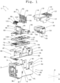
- FIG. 1 An electrical connector 1 is shown, which is designed as a socket 2.
- the socket 2 has a housing 10, wherein the housing 10 can be divided into an upper housing part 90 and a lower housing part 12. Both the lower housing part 12 and the upper housing part 90 are made of a conductive material, in particular of a metal housing 10. This ensures the electromagnetic compatibility and reduces electromagnetic interference.
- the metal housing 10 can be formed, for example, from sheet metal or a die-cast metal part, in particular a zinc die-cast part.
- the lower housing part 12 has a front side 3 and a rear side 4, wherein the front side 3 is the side into which a complementary plug is inserted and the rear side 4 is the side into which a cable (not shown) is inserted into the socket 2.
- the front side 3 has a window for this purpose, which has the typical shape of an RJ45 plug.
- the lower housing part 90 has a base 91 and, starting from the base 91, two side surfaces 92 pointing towards the upper housing part 11. The base 91 and the two side surfaces 92 connect the front side 3 and the rear side 4 to one another.
- the rear side 4 has an open surface 93.
- the lower housing part 90 has a roof 94.
- the roof 94 runs parallel to the base 91.
- the spatial plane in which the base 91 of the lower housing part 90 is arranged is defined as the underside 6 of the socket 2.
- the spatial plane in which the roof 94 is arranged is defined as the top side 5 of the socket 2.
- Each side surface 92 has an L-shaped bulge 95.
- the side surface 92 has holding means, which are preferably designed as bulges 96-98. A total of three bulges 96-98 are formed on each side surface 92.
- the first bulge 96 is arranged in the area of the rear side 4 and top side 5.
- the second bulge 97 is arranged in the middle of the side surface 92 and the third bulge 98 is arranged in the central region near the front side 3.
- a shielding part 80 is arranged within the lower housing part 90.
- the shielding part 80 has a base plate 81, wherein the base plate 81 rests on the bottom 91 of the lower housing part 90.
- the base plate 81 forms a fastening element 88 on the front edge, which points in the direction of the underside 6 of the socket 2.
- the shielding part 80 is fixed to the lower housing part 90 by the fastening element 88 and by a complementary holding means (not shown) of the lower housing part 90.
- the shielding part 80 Near the rear side 4, the shielding part 80 has two first outer surfaces 82, wherein the first outer surfaces 82 run parallel to the side surfaces 92 of the lower housing part 90.
- the two first outer surfaces 82 are connected to one another in the region of the upper side 5 via an overhang 84.
- the overhang 84 has an arcuate shape, with the arcuate shape of the overhang 84 decreasing towards the interior of the socket 2.
- the overhang 84 is arranged closer to the rear side 4 than the loading piece 50.
- the roof also has a fixing element 16 which projects beyond the rear side 4 of the socket 2. Using a cable tie (not shown) and the fixing element 16, the cable to be inserted can be additionally mechanically fixed to the socket 2.
- first outer surfaces 82 have holding means in the form of first locking lugs 85.
- the first locking lugs 85 point towards the interior of the socket 2.
- two L-shaped second outer surfaces 83 are arranged.
- the second outer surfaces 83 run parallel to the side surfaces 92 of the housing base 90.
- At the free end of the L-shaped A retaining lug 87 is arranged on the second outer surface 83, which points in the direction of the side surfaces 92 of the lower housing part 90. In the assembled state, the retaining lug 87 engages in the third bulge 98 of the lower housing part 90.
- the L-shaped second outer surfaces 83 are pressed in the direction of the side surfaces 92 of the lower housing part 90, whereby the retaining lugs 87 are pressed more firmly into the third bulge 98 of the lower housing part 90.
- the shielding part 80 and the shielding of the connector make contact, among other things, via the L-shaped second outer surfaces 83.
- the shielding transfer from the socket 2 to the connector takes place in this area.
- the second outer surfaces 83 have holding means in the form of second locking lugs 86.
- the second locking lugs 86 point in the direction of the interior of the socket 2.
- the upper housing part 11 is U-shaped. It has a roof 12, which is arranged in the space in the upper side 5 of the socket 2.
- the roof 12 has a canopy 13, which, when assembled, nestles into a protrusion 99 of the roof 94 of the lower housing part 90.
- the upper housing part 11 has a side wall 14, wherein a portion of the side wall 14 is L-shaped and nestles into the L-shaped bulge 95 of the side surface 92 of the lower housing part 90 when assembled.
- the region of the side wall 14 that is arranged closer to the rear side 4 is indented towards the center of the socket 2 and has a retaining means, which is preferably designed as a nose 15.
- the upper housing part 11 can be connected to the lower housing part 90 by means of a snap-fit connection.
- the nose 15 of the upper housing part 11 engages in the first bulge 96 of the lower housing part 90.
- a charging piece 50 is arranged in the upper housing part 11, wherein the charging piece 50 is made of a non-electrically conductive material, in particular of plastic.
- the body of the charging piece 50 is L-shaped.
- the first leg 51 of the L-shaped body which runs parallel to the top side 5 of the socket 2, preferably has four through-holes 52 through which the individual wires of the cable to be inserted are passed.
- guides 54 are arranged in the first leg 51, through which a row of insulation displacement terminals 31 can be passed.
- the second leg 53 of the L-shaped body stands perpendicular to the top side 5 of the socket 2 and has cavities 55.
- First contact elements 30, which are preferably designed as insulation displacement terminals 31, can be inserted through the guides 54 of the first leg 51 and the recesses 55 of the second leg 52.
- the insulation displacement terminals 31 penetrate the guides 54 or recesses 55, thereby stripping the individual wires of the inserted cable and establishing an electrical connection.
- the insulation displacement terminals 31 are arranged near the rear side 4.
- the insulation displacement terminals 31 point towards the upper housing part 11.
- the insulation displacement terminal 31 has a foot 110, which can be passed through a first through-opening 115.
- the foot 110 of the insulation displacement terminal 31 is electrically and mechanically contacted by means of soldering or pressing with the first contact pad 117.
- the insulation displacement terminal 31 has a hole 34 in its center.
- the insulation displacement terminals 31 are arranged in two rows, wherein a row is characterized in that the feet 110 of the insulation displacement terminals 31 in one row are arranged at the same distance from the rear side 4 of the connector.
- the insulation displacement terminals 31 can be arranged in one row or in more than one row, for example in two, three, four, or five rows.
- the insulation displacement terminal surfaces 32 are aligned parallel to one another in the present case.
- the insulation displacement terminal surfaces 32 of different rows can be at an angle to one another.
- the insulation displacement terminal surfaces 32 of insulation displacement terminals 31 in one row can be at different angles to one another.
- the insulation displacement terminal surfaces 32 can be perpendicular to one another.
- the insulation displacement terminals 31 in one row can have a different height than the insulation displacement terminals 31 in another row, with the height of an insulation displacement terminal 31 being the distance between the point on the insulation displacement terminal 31 into which a cable can be inserted and the top of the circuit board.
- the insulation displacement terminals 31 within a row can have different heights from one another. This makes it possible to design the socket 2 more compactly, since the installation space is optimized by arranging the individual wires one above the other in the charging piece 50.
- Each insulation displacement terminal 31 is electrically connected to a second contact element 35, which is preferably designed as a plug contact 36, via a conductor track 21.
- the plug contacts 36 are arranged near the front side 3 of the socket 2.
- the plug contacts 36 have a foot 111 which fits into a second through-opening 116 on the
- the printed circuit board 20 is guided and is mechanically fixed and electrically contacted by means of pressing and/or soldering.
- the plug contacts 36 are pin-shaped, with the plug contacts 36 projecting upwards toward the rear side 4 of the socket 2.
- the plug contacts 36 connected to conductor tracks three 103 and six 106 are shorter than the other plug contacts 36.
- the plug contacts 36 are spring-loaded.
- a support element 60 Arranged above the circuit board 20 is a support element 60 having recesses 61 through which the insulation displacement terminals 31 are guided.
- a raised portion 62 is formed, which, when assembled, touches the roof 12 of the upper housing part 11.
- a first notch 64 is arranged on the outer surface 63 of the raised portion 62, into which the second locking lug 86 of the shielding part 80 engages.
- a further second notch 65 is formed, into which the first locking lug 85 of the shielding part 80 engages. The engagement of the two locking lugs 85, 86 mechanically fixes the support element 60 to the shielding part 80.
- the carrier element 60 has, in the region of the rear side 4 on its lower side, two pins 66 which can be inserted into two complementary holes 27 on the printed circuit board 20 and two indentations 72 in the cover 70 and prevent displacement along a plane.
- the cover 70 is arranged below the circuit board 20.
- the cover 70 has rails 73 that rest on the base plate 81 of the shielding part 80. Furthermore, the cover 70 has recesses 71, 74 into which the feet 110, 111 of the plug contacts 36 and the insulation displacement terminals 31, which extend through the circuit board 20, can penetrate.
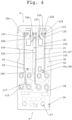
- the printed circuit board 20 is depicted with plug contacts 36 and insulation displacement terminals 31 arranged thereon.
- the plug contacts 36 are arranged in two rows, with the number of plug contacts 36 varying within a row.
- the row arranged closer to the front 3 of the socket 2 has six plug contacts 36, whereas the row arranged further from the front 3 of the socket 2 has two plug contacts 36.
- the number of rows and the number of plug contacts 36 within a row are variable.
- the plug contacts 36 in the second row are shorter than the other plug contacts 36.
- the plug contacts 36 can reach different heights with respect to the printed circuit board 20 and can protrude different distances towards the center of the circuit board.
- each conductor track 21 connects an insulation displacement terminal 31 to a plug contact 36.
- a conductor track 21 has a first contact pad 117 and a second contact pad 118, which are arranged around a first through-opening 115 and a second through-opening 116 and are electrically connected via a conductor path 25.
- the conductor path 25 can run over different circuit board layers 26 and have different conductor track widths. It has proven advantageous that, starting from the insulation displacement terminal 31, the width of the conductor track 21 becomes increasingly smaller and the distance between the conductor tracks 21, for example of a differential line 22, increases. This is advantageous because the impedance of the insulation displacement terminal 31 is significantly greater than the Impedance of the plug contact 36 and with a step-by-step adjustment of the impedance of the line path 25, the insertion loss and return loss are significantly improved.
- the circuit board 20 has eight conductor tracks 21.
- Two conductor tracks 21 each form a differential line 22, whereby a distinction is made between the first conductor track 23 and the second conductor track 24 for the two conductor tracks 21 of a differential line 22.
- four first conductor tracks 23 and four second conductor tracks 24 are arranged on the circuit board 20.
- the four first conductor tracks 23 are defined as conductor track one 101, conductor track three 103, conductor track five 105, and conductor track seven 107
- the second conductor tracks 24 are defined as conductor track two 102, conductor track four 104, conductor track six 106, and conductor track eight 108.
- Conductor track one 101 and conductor track two 102 form a first differential line 121.
- Conductor track three 103 and conductor track six 106 form a second differential line 122.
- Conductor track four 104 and conductor track five 105 form a third differential line 123, and conductor track seven 107 and conductor track eight 108 form a fourth differential line 124.
- the conductor tracks 21 of a differential line 22 can run on different circuit board layers 26, with the individual sections of the conductor tracks on the different circuit board layers 26 usually being connected by means of vias 29.
- the circuit board 20 has a total of nine compensation units 125, wherein the compensation units 125 are configured as plate capacitors 126.
- a plate capacitor 126 has two conductive plates 127 running parallel to one another. A dielectric is arranged between the plates 127.
- the capacitance of the plate capacitor 126 can be varied by selecting the circuit board layers 26 on which the plates 127 of the plate capacitor 126 are arranged. The capacitance can also be varied by changing the surface area of the plates 127 of the plate capacitor 126.
- the plates 127 of the plate capacitors 126 are preferably square and arranged almost completely overlapping one another. However, the plates 127 can also be polygonal, round, or oval.
- the plates 127 of the plate capacitors 126 are connected, for example, to a conductor track 21 via stub lines 28.
- the stub line 28 can be connected to a contact pad 117, 118 or the conductor path 25.
- Two of the nine plate capacitors 126 are connected between conductor track one 101 and conductor track three 103, with one plate capacitor 126 located near the insulation displacement terminals 31 and the other plate capacitor 126 located near the plug contacts 36. Another plate capacitor 126 is connected between conductor track six 106 and conductor track eight 108. Another plate capacitor 126 is connected between conductor track four 104 and conductor track six 106. Another plate capacitor 126 is connected between conductor track three 103 and conductor track five 105. Another plate capacitor 126 is connected between conductor track five 105 and conductor track six 106. Another plate capacitor 126 is connected between conductor track two 102 and conductor track four 104. Another plate capacitor 126 is connected between the conductor track four 104 and the conductor track eight 108. Another Plate capacitor 126 is connected between conductor track three 103 and conductor track seven 107. The plate capacitors 126 can also be designed as interdigital capacitors.
- the conductive surfaces 40 are formed in the inner circuit board layers 26. However, conductive surfaces 40 can also be arranged in the uppermost circuit board layer 26 and in the lowermost circuit board layer 26. A total of forty-six conductive surfaces 40 are arranged on the circuit board 20. However, more or fewer conductive surfaces 40 can also be arranged on the circuit board 20. Furthermore, a different number of conductive surfaces 40 can be arranged on the individual circuit board layers 26, in particular on the inner circuit board layers 26. The number of conductive surfaces 40 is selected such that the conductive surfaces 40 are preferably not arranged overlapping a conductive surface of the circuit, in particular the signal paths.
- the signal path is defined as the path which transmits a signal through the socket 2 on a direct path.
- the conductive surface 40 can be arranged overlapping a conductor track 21, in particular a signal path. However, the conductive surface 40 should not be arranged to overlap more than one signal path, since the influence on the impedance and thus on the insertion loss and return loss, as well as on the compensation circuit, would be too great and a change in the circuit design would be necessary to ensure the same transmission performance and comply with the standard requirements.
- Several conductive surfaces 40 can overlap a conductive path 25 or a contact pad 117, 118.
- a conductive surface 40 does not overlap two conductive paths 25 or two contact pads 117, 118, or a conductive path 25 and a contact pad 117, 118.
- the conductive surfaces 40 have no influence at all or no measurable influence on the conductive surfaces on the Printed circuit board 20, this is achieved in particular by the fact that no conductive surface 40 is arranged below or above a conductive path 25 or contact pads 117, 118.
- the conductive surfaces 40 can be arranged overlapping the compensation units 125, which are preferably designed as plate capacitors 126. The influence of the conductive surfaces 40 on the capacitances of the plate capacitors 126 is usually negligible. Likewise, one conductive surface 40 or several conductive surfaces 40 can be arranged overlapping to form a stub line 28. It is irrelevant whether the stub line 28 is connected to a contact pad 117, 118 or to a conduction path 25.
- the conductive surfaces 40 are designed such that they are small enough to overlap one or no conductor tracks 21, yet large enough to provide stability to the layer structure. Furthermore, as much of a printed circuit board layer 26 as possible should be covered with conductive surfaces 40. A minimum distance from the edge of the printed circuit board layer 26 is preferably maintained. However, the conductive surfaces 40 can also be arranged directly at the edge of a printed circuit board layer 26.
- the conductive surfaces 40 are preferably arranged in rows 41 on the circuit board 20, but can also be arranged individually on the circuit board 20.
- a row 41 has at least two conductive surfaces 40, wherein the conductive surface centers 43 of the conductive surfaces 40 of a row 41 lie on an imaginary line, wherein the line is arranged parallel to the longitudinal axis L or to the width axis B.
- the longitudinal axis L is orthogonal to the width axis B and the transverse axis Q.
- a conductive surface 40 can be part of two or more rows 41.
- the circuit board 20 has thirty-two Rows 41, with each circuit board layer 26 forming sixteen rows 41.
- each circuit board layer 26 four rows 41 with three conductive surfaces 40, eleven rows 41 with two conductive surfaces 40, and one row 41 with five conductive surfaces 40 are formed. Ten rows 41 are formed on an imaginary line arranged parallel to the longitudinal axis L, and six rows 41 are formed on an imaginary line arranged parallel to the width axis B.
- the arrangement of the conductive surfaces 40 gives the circuit board layer structure even more stability.
- the conductive surfaces 40 can also be arranged offset from one another, whereby areas that are critical with regard to the stability of the layer structure are specifically reinforced.
- the arrangement of conductive surfaces 40 can be arranged in groups. At least one group 42 can be arranged on the circuit board 20.
- a group 42 has at least two overlapping, preferably completely overlapping, rows 41.
- a group 42 does not have to use every member of a row 41 to be considered a group 42. However, at least two members of a row 41 must be involved in forming a group 42.
- the members of group 42 do not have to be adjacent to one another.
- the topmost circuit board layer 26 is indicated by solid lines, and the underlying circuit board layers 26 are indicated by dashed lines.
- the compensation units 125 are clearly visible, with the plates 127 of most of the plate capacitors 126 arranged completely overlapping each other.
- the two holes 27 are arranged, through which the pins 66 of the carrier element 60 are guided, thus preventing displacement of the circuit board 20. within a plane.
- the second contact pads 118 are significantly smaller than the first contact pads 117. Both contact pads 117, 118 are oval-shaped.
- Conductor tracks one 101 and two 102 of the first differential line 121 are arranged to completely overlap one another in sections. The same applies to the fourth differential line 124.
- conductor tracks five 105 and six 106 run over one another in sections, as do conductor tracks three 103 and four 104.
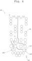
- the inner circuit board layers 26 are shown.
- the conductive surfaces 40 are clearly visible.
- the conductive surfaces 40 can be round as shown, but also oval or polygonal, in particular square, or have the shape of a parallelogram or a trapezoid.
- the conductive surfaces 40 are designed such that as many conductive surfaces as possible and as large as possible can be arranged on the circuit board 20. To achieve this, the conductive surfaces 40 must adapt to the circuit design and adjust their shape accordingly.
- the plates 127 of a plate capacitor 126 are never arranged on adjacent inner circuit board layers 26.
- the plates 127 of a plate capacitor 126 can also be arranged on adjacent inner circuit board layers 26.
Landscapes
- Physics & Mathematics (AREA)
- Electromagnetism (AREA)
- Engineering & Computer Science (AREA)
- Microelectronics & Electronic Packaging (AREA)
- Details Of Connecting Devices For Male And Female Coupling (AREA)
Abstract
Elektrischer Verbinder für ein Datenkabel mit folgenden Merkmalen:- ein Gehäuse (10),- eine zumindest teilweise im Gehäuse (10) angeordneten Leiterplatte (20), wobei die Leiterplatte (20) als mehrlagige Leiterplatte ausgebildet ist.- erste Kontaktelemente (30) und zweite Kontaktelemente (35), wobei diese über eine Leiterbahn (21) miteinander verbunden sind, wobei die Leiterbahn (21) einen Leitungspfad (25) und Kontaktpads (117, 118) aufweist.gekennzeichnet durch die weiteren Merkmale:- die Leiterplatte (20) bildet Leitflächen (40) aus, wobei jede Leitfläche (40) von anderen leitenden Flächen elektrisch isoliert ist,- die Leitflächen (40) sind auf den inneren Leiterplattenlagen (26) angeordnet,- eine innere Leiterplattenlage (26) weist mindestens drei Leitflächen (40) auf, und- die Leitfläche (40) ist höchstens zu einem Leitungspfad (25) überlappend angeordnet.Electrical connector for a data cable, having the following features:- a housing (10),- a printed circuit board (20) arranged at least partially in the housing (10), the printed circuit board (20) being designed as a multi-layer printed circuit board.- first contact elements (30) and second contact elements (35), said first contact elements being connected to one another via a conductor track (21), the conductor track (21) having a conducting path (25) and contact pads (117, 118).characterized by the further features:- the printed circuit board (20) forms conductive surfaces (40), each conductive surface (40) being electrically insulated from other conductive surfaces,- the conductive surfaces (40) are arranged on the inner printed circuit board layers (26),- an inner printed circuit board layer (26) has at least three conductive surfaces (40), and- the conductive surface (40) is arranged so as to overlap at most one conducting path (25).
Description
Die Erfindung betrifft einen elektrischen Verbinder für ein Datenkabel gemäß den Merkmalen des Anspruchs 1.The invention relates to an electrical connector for a data cable according to the features of
Bei elektrischen Verbindern, insbesondere im Bereich der Hochfrequenztechnik, weisen Leiterplatten floatende Masseflächen auf, wobei die Masseflächen sich über nahezu die gesamte Leiterplattenlage erstrecken. Diese Masseflächen sollen insbesondere das EMV-Verhalten verbessern, Crosstalk reduzieren oder die Impedanzen von Leitungen oder Bauteilen beeinflussen. Ein elektrischer Verbinder, welcher eine Leiterplatte mit Massefläche aufweist, um das EMV-Verhalten zu verbessern, Crosstalk zu reduzieren oder die Impedanzen von Leitungen oder Bauteilen zu beeinflussen, ist aus
Zusätzlich zu den genannten Vorteilen hat eine Massefläche einen positiven Effekt auf die Stabilisation des Lagenaufbaus einer Leiterplatte. Um diese zu verbessern und gleichzeitig das Schaltungsdesign einer bestehenden Schaltung beizubehalten, dürfen die Masseflächen kaum bis keinen Einfluss auf die bestehende Schaltung aufweisen.In addition to the aforementioned advantages, a ground plane has a positive effect on stabilizing the layer stack of a printed circuit board. To improve this while maintaining the circuit design of an existing circuit, ground planes must have little to no impact on the existing circuit.
Dieses Problem wird durch einen elektrischen Verbinder mit den Merkmalen des Patentanspruchs 1 gelöst.This problem is solved by an electrical connector having the features of
Vorteilhafte Ausgestaltungen und Weiterbildungen der Erfindung sind in den abhängigen Ansprüchen angegeben.Advantageous embodiments and further developments of the invention are specified in the dependent claims.
Erfindungsgemäß ist demnach ein elektrischer Verbinder für ein Datenkabel mit einem Gehäuse und eine zumindest teilweise im Gehäuse angeordnete Leiterplatte, wobei die Leiterplatte als mehrlagige Leiterplatte ausgebildet ist. An der Leiterplatte sind erste Kontaktelemente und zweite Kontaktelemente angeordnet, wobei diese jeweils über eine Leiterbahn miteinander verbunden sind. Eine Leiterbahn weist einen Leitungspfad und Kontaktpads auf. Die Leiterplatte weist elektrisch isolierte Leitflächen auf. Die Leitflächen sind dabei auf mindestens einer inneren Leiterplattenlage angeordnet, wobei eine innere Leiterplattenlage mindestens drei Leitflächen aufweist und die Leitfläche höchstens zu einem Leitungspfad überlappend angeordnet ist.According to the invention, an electrical connector for a data cable is provided with a housing and a printed circuit board arranged at least partially in the housing, wherein the printed circuit board is designed as a multilayer printed circuit board. First contact elements and second contact elements are arranged, each of which is connected to one another via a conductor track. A conductor track has a conducting path and contact pads. The circuit board has electrically insulated conductive surfaces. The conductive surfaces are arranged on at least one inner circuit board layer, wherein an inner circuit board layer has at least three conductive surfaces and the conductive surface is arranged so as to overlap at most one conducting path.
Die Leitflächen sind inselförmig und elektrisch isoliert auf der Leiterplatte angeordnet. Inselförmig meint dabei, dass die Leitfläche mit keiner anderen leitenden Fläche verbunden ist. Leitende Flächen können dabei andere Leitflächen, Leiterbahnen, Stichleitungen, Kompensationseinheiten und weitere sein. Eine Überlappung der Leitfläche mit dem signalführenden Leitungspfad und/oder den Kontaktpads verändert unter Umständen einige Parameter im verwendeten Schaltungsdesign. Um eine Stabilisierung des Lagenaufbaus zu erreichen, ohne einige Parameter zu verändern, werden Leitflächen derart auf den inneren Leiterplattenlagen der Leiterplatte angeordnet, sodass die Leitflächen groß genug sind, um eine stabilisierende Wirkung zu erzeugen, jedoch klein genug sind, sodass die Leitfläche nicht mit mehr als einem Leitungspfad überlappend angeordnet ist. Würde eine Leitfläche mehr als einen Leitungspfad überlappen, so wäre der Einfluss der Leitfläche auf die Hochfrequenzübertragungsparameter zu groß und das Schaltungsdesign müsste abgeändert werden, was wiederrum den Entwicklungsaufwand und damit die Kosten erhöht.The conductive surfaces are arranged in islands and are electrically isolated on the circuit board. "Island-like" means that the conductive surface is not connected to any other conductive surface. Conductive surfaces can be other conductive surfaces, traces, stubs, compensation units, and others. An overlap of the conductive surface with the signal-carrying conductive path and/or the contact pads may change some parameters in the circuit design used. To stabilize the layer stack without changing some parameters, conductive surfaces are arranged on the inner PCB layers in such a way that the conductive surfaces are large enough to create a stabilizing effect, but small enough that the conductive surface does not overlap with more than one conductive path. If a conductive surface were to overlap more than one conductive path, the influence of the conductive surface on the high-frequency transmission parameters would be too great, and the circuit design would have to be modified, which in turn increases development effort and thus costs.
Vorteilhafterweise bilden jeweils zwei Leiterbahnen eine differentielle Leitung aus, wobei eine Leiterbahn ein erstes und zweites Kontaktpad aufweist, welche über einen Leitungspfad miteinander verbunden sind.Advantageously, two conductor tracks each form a differential line, wherein a conductor track has a first and a second contact pad which are connected to one another via a conduction path.
Die Kontaktelemente sind in erste und zweite Kontaktelemente unterteilbar, wobei die ersten Kontaktelemente vorzugsweise als Schneidklemmen und die zweiten Kontaktelemente als Steckkontakte ausgebildet sind. Die Kontaktpads sind ebenfalls in erste und zweite Kontaktpads unterteilbar, wobei die ersten Kontaktelemente direkt mit den ersten Kontaktpads verbunden sind, und wobei die zweiten Kontaktelemente direkt mit den zweiten Kontaktpads verbunden sind. Die ersten und zweiten Kontaktpads sind um erste und zweite Durchgangsöffnungen herum ausgebildet. Ein Kontaktpad kann auf mehreren Leiterplattenlagen ausgebildet sein. Die Durchgangsöffnungen sind an den Rändern verkupfert, wobei diese verkupferten Ränder die einzelnen Ebenen des Kontaktpads miteinander verbinden, und Teil eines Kontaktpads sind. Die Kontaktpads können die Form eines Kreises, eines Ovals, eines Vierecks aufweisen.The contact elements can be divided into first and second contact elements, wherein the first contact elements are preferably designed as insulation displacement contacts and the second contact elements as plug contacts. The contact pads can also be divided into first and second contact pads, wherein the first contact elements are directly connected to the first contact pads and wherein the second contact elements are directly connected to the second contact pads. The first and second contact pads are formed around first and second through-openings. A contact pad can be formed on multiple circuit board layers. The through-openings are copper-plated at the edges, wherein these copper-plated edges connect the individual levels of the contact pad to one another and are part of a contact pad. The contact pads can have the shape of a circle, an oval, or a square.
Die ersten Kontaktelemente sind als Schneidklemmen ausgebildet. Schneidklemmen, welche auch IDC genannt werden, zeichnen sich dadurch aus, dass eine schnelle und einfache Installation bewerkstelligbar ist. Die Drähte können mithilfe der Schneidklemmen elektrisch kontaktiert werden, ohne dass die Isolation gesondert entfernt werden muss, wodurch Zeit und die Fehleranfälligkeit sinken. Zudem werden keine speziellen Werkzeuge zur Abisolierung der Drähte benötigt. Schneidklemmen zeichnen sich durch eine äußerst zuverlässige Verbindung aus. Beim Zusammensetzten durchschneiden die Klemmen der Schneidklemme die Isolierung, wodurch eine gasdichte Verbindung zwischen Draht und Schneidklemme entsteht und ein Eindringen von Feuchtigkeit und anderen Kontaminationen verhindert wird.The first contact elements are designed as insulation displacement connectors. Insulation displacement connectors, also known as IDCs, are characterized by their quick and easy installation. The wires can be electrically connected using the insulation displacement connectors without having to remove the insulation, thus reducing time and the risk of errors. Furthermore, no special tools are required to strip the wires. Insulation displacement connectors are characterized by an extremely reliable connection. When assembled, the terminals of the insulation displacement connector cut through the insulation, creating a gas-tight connection between the wire and the insulation displacement connector, preventing the ingress of moisture and other contaminants.
In elektrischen Verbindern findet die Datenübertragung vorzugsweise auf differentiellen Leitungen statt. Eine differentielle Leitung weist eine erste Leiterbahn und eine zweite Leiterbahn auf. Die häufig als Plus-Leiterbahn oder Tip-Leiterbahn benannte Leiterbahn ist hier und im Folgenden die erste Leiterbahn, wohingegen die Minus-Leiterbahn oder auch Ring-Leiterbahn hier und im Folgenden als zweite Leiterbahn definiert ist. Auf der ersten Leiterbahn wird ein Signal übertragen, während die zweite Leiterbahn das invertierte Signal transmittiert. Der Empfänger bildet die Differenz zwischen den beiden Signalen, wobei die Differenz dem ursprünglichen zu übertragenden Signal entspricht.In electrical connectors, data transmission preferably takes place on differential lines. A differential line has a first conductor track and a second conductor track The track, often referred to as the positive track or tip track, is the first track here and below, whereas the negative track or ring track is defined here and below as the second track. A signal is transmitted on the first track, while the second track transmits the inverted signal. The receiver calculates the difference between the two signals, which corresponds to the original signal to be transmitted.
Auf der Leiterplatte sind vier differentielle Leitungen ausgebildet, es können allerdings auch mehr oder weniger differentielle Leitungen ausgebildet sein. Jeweils eine erste und eine zweite Leiterbahn bilden dabei eine differentielle Leitung aus. Die Leiterbahnen sind von eins bis acht definiert, wobei die Leiterbahnen eins und zwei, die Leiterbahnen drei und sechs, die Leiterbahnen vier und fünf und die Leiterbahnen sieben und acht jeweils eine differentielle Leitung ausbilden. Auf der Leiterplatte sind zudem Kompensationseinheiten in Form von Plattenkondensatoren angeordnet, wobei die Plattenkondensatoren auch als Interdigitalkondensatoren ausgestaltet sein können. Die Kapazität eines Plattenkondensators ist in einem vereinfachten Modell direkt proportional zur relativen Permittivität des Dielektrikums und zur kleinsten Plattenfläche. Zudem ist die Kapazität reziprok zum Abstand der Platten zueinander.Four differential lines are formed on the circuit board, although more or fewer differential lines can also be formed. A first and a second conductor track each form a differential line. The conductor tracks are defined from one to eight, with conductor tracks one and two, conductor tracks three and six, conductor tracks four and five, and conductor tracks seven and eight each forming a differential line. Compensation units in the form of plate capacitors are also arranged on the circuit board; the plate capacitors can also be designed as interdigital capacitors. In a simplified model, the capacitance of a plate capacitor is directly proportional to the relative permittivity of the dielectric and to the smallest plate area. Furthermore, the capacitance is reciprocal to the distance between the plates.
Gemäß einer vorteilhaften Ausgestaltung der Erfindung sind auf einer inneren Leiterplattenlage mehr oder gleich viele Leitflächen ausgebildet als auf der anderen inneren Leiterplattenlage. Es kann auch auf einer inneren Leiterplattenlage keine Leitfläche ausgebildet sein. Weist die Leiterplatte mehr als 2 innere Leiterplattenlagen auf, kann auch auf mehr als einer Leiterplattenlage keine Leitfläche ausgebildet sein.According to an advantageous embodiment of the invention, more or the same number of conductive surfaces are formed on one inner circuit board layer than on the other inner circuit board layer. No conductive surface may be formed on an inner circuit board layer. If the circuit board has more than two inner circuit board layers, no conductive surface may be formed on more than one circuit board layer.
Gemäß einer besonders bevorzugten Ausgestaltung der Erfindung macht die Fläche der Leitfläche maximal annähernd zwischen 0,5 % bis 100 % der Fläche der Leiterplattenlage aus. Vorzugsweise beträgt die Fläche der Leitfläche maximal annähernd 100 %, bevorzugt 75 %, besonders bevorzugt 35 %, im Besonderen bevorzugt 15 %, ganz besonders bevorzugt 5 %, im äußersten bevorzugt 2 %, im aller äußersten bevorzugt 1 %, am bevorzugtesten 0,5 % der Fläche der Leiterplattenlage.According to a particularly preferred embodiment of the invention, the area of the conductive surface makes up a maximum of approximately between 0.5% and 100% of the area of the printed circuit board layer. Preferably, the area of the conductive surface is a maximum of approximately 100%, preferably 75%, particularly preferably 35%, particularly preferably 15%, very particularly preferably 5%, most preferably 2%, most preferably 1%, most preferably 0.5% of the area of the printed circuit board layer.
Vorteilhafterweise macht die Gesamtfläche aller Leitflächen mindestens annähernd zwischen 2 % bis 125 % der Fläche der Leiterplattenlage aus. Vorzugsweise beträgt die Gesamtfläche aller Leitflächen mindestens annähernd 2 %, besonders bevorzugt 5 %, im Besonderen bevorzugt 15 %, ganz besonders bevorzugt 30 %, im äußersten bevorzugt 75 %, im aller äußersten bevorzugt 125 % der Fläche der Leiterplattenlage.Advantageously, the total area of all conductive surfaces amounts to at least approximately between 2% and 125% of the surface area of the printed circuit board layer. Preferably, the total area of all conductive surfaces amounts to at least approximately 2%, particularly preferably 5%, particularly preferably 15%, very particularly preferably 30%, most preferably 75%, and most preferably 125% of the surface area of the printed circuit board layer.
In einer vorteilhaften Weiterbildung der Erfindung macht die Gesamtfläche aller Leitflächen auf einer Leiterplattenlage mindestens annähernd zwischen 2 % bis 100 % der Fläche der Leiterplattenlage aus. Vorzugsweise beträgt die Gesamtfläche aller Leitflächen auf einer Leiterplattenlage mindestens annähernd 2 %, besonders bevorzugt 5 %, im Besonderen bevorzugt 10 %, ganz besonders bevorzugt 20 %, im äußersten bevorzugt 50 %, im aller äußersten bevorzugt 100 %, der Fläche der Leiterplattenlage. Ziel ist es, so viele Leitflächen mit einer möglichst großen Fläche auf einer oder mehrerer Leiterplattenlagen auszubilden, um dadurch eine möglichst große Stabilität des Leiterplattenaufbaus zu erzielen.In an advantageous development of the invention, the total area of all conductive surfaces on a printed circuit board layer makes up at least approximately between 2% and 100% of the surface area of the printed circuit board layer. Preferably, the total area of all conductive surfaces on a printed circuit board layer is at least approximately 2%, particularly preferably 5%, particularly preferably 10%, very particularly preferably 20%, most preferably 50%, most preferably 100%, of the surface area of the printed circuit board layer. The goal is to form as many conductive surfaces with the largest possible surface area on one or more printed circuit board layers in order to achieve the greatest possible stability of the printed circuit board structure.
Gemäß einer bevorzugten Ausgestaltung der Erfindung weist die Leitfläche die Form eines Ovals oder eines Kreises oder eines Vielecks, vorzugsweise eines Vierecks oder Dreiecks oder eines Trapezes oder eines Kreises oder eines Parallelogramms, auf. Innerhalb der Leitflächen können Freiflächen ausgebildet sein, insbesondere dann, wenn überlappend zu den Freiflächen eine Leiterbahn ausgebildet ist. Die Freiflächen können jegliche Form und Größe annehmen. Auch kann eine solche Freifläche am Rand angeordnet sein, sodass innerhalb der Leitfläche eine Auskerbung ausgebildet ist. Die Auskerbung kann rund, eckig oder ähnliches sein. Die Leitfläche ist stets so ausgebildet, dass diese sich an die Umgebung auf der Leiterplatte anpasst und möglichst zu keinem signalführenden Bereich überlappend angeordnet ist. Zudem kann innerhalb der Freifläche der Leitfläche ein Via durchgeführt werden. Dazu darf das leitende Material des Vias einen normativ festgelegten Mindestabstand zu der Leitfläche nicht unterschreiten. Es können zwei oder mehr Vias in einer oder mehrerer Freiflächen einer Leitfläche angeordnet werden.According to a preferred embodiment of the invention, the guide surface has the shape of an oval or a circle or a polygon, preferably a square or triangle or a trapezoid, circle, or parallelogram. Open spaces can be formed within the conductive surfaces, particularly when a conductor track is formed that overlaps the open spaces. The open spaces can take on any shape and size. Such an open space can also be arranged at the edge, so that a notch is formed within the conductive surface. The notch can be round, square, or similar. The conductive surface is always designed in such a way that it adapts to the surroundings on the circuit board and, if possible, does not overlap with any signal-carrying area. In addition, a via can be made within the open space of the conductive surface. For this purpose, the conductive material of the via must not be less than a standardized minimum distance from the conductive surface. Two or more vias can be arranged in one or more open spaces of a conductive surface.
In einer besonders günstigen Ausgestaltung der Erfindung sind vorzugsweise mehr als fünf, besonders bevorzugt mehr als zehn, ganz besonders bevorzugt mehr als zwanzig, im äußersten bevorzugt mehr als fünfzig, im aller äußersten bevorzugt mehr als einhundert Leitflächen auf der Leiterplatte angeordnet.In a particularly advantageous embodiment of the invention, preferably more than five, particularly preferably more than ten, very particularly preferably more than twenty, extremely preferably more than fifty, extremely preferably more than one hundred conductive surfaces are arranged on the printed circuit board.
In einer vorteilhaften Weiterbildung der Erfindung sind zumindest zwei Leitflächen auf unterschiedlichen Leiterplattenlagen vollständig überlappend zueinander angeordnet. Es können allerdings auch mehr als zwei Leitflächen vollständig überlappend zueinander angeordnet sein. Vorzugsweise sind alle Leitflächen überlappend zueinander angeordnet. Wird eine Leiterplatte verwendet, welche mehr als zwei innere Leiterplattenlagen aufweist, so können auch drei oder mehr Leitflächen, welche auf drei oder mehr Leiterplattenlagen angeordnet sind, überlappend beziehungsweise vollständig überlappend zueinander angeordnet sein.In an advantageous development of the invention, at least two conductive surfaces on different circuit board layers are arranged so as to completely overlap one another. However, more than two conductive surfaces can also be arranged so as to completely overlap one another. Preferably, all conductive surfaces are arranged so as to overlap one another. If a circuit board is used that has more than two inner circuit board layers, three or more conductive surfaces arranged on three or more circuit board layers can also be arranged so as to overlap or completely overlap one another.
Gemäß einer besonders bevorzugten Ausgestaltung der Erfindung ist keine Leitfläche zu einem Leitungspfad überlappend angeordnet. Vorzugsweise ist keine Leitfläche zu einem signalführenden Bauteil, insbesondere dem Leitungspfad und den Kontaktpads, überlappend angeordnet. Vorzugsweise ist auch keine Leitfläche zu einer Stichleitung oder Kompensationseinheit überlappend angeordnet. Eine Überlappung der Leitfläche, insbesondere mit signalführenden Pfaden, würde die Schaltungseigenschaften beeinflussen, was sich negativ auf die Übertragungsleistung auswirken könnte und eine Abänderung des Schaltungsdesigns eventuell nach sich ziehen müsste.According to a particularly preferred embodiment of the invention, no conductive surface is arranged to overlap a conduction path. Preferably, no conductive surface is arranged to overlap a signal-carrying component, in particular the conduction path and the contact pads. Preferably, no conductive surface is arranged to overlap a stub line or compensation unit. An overlap of the conductive surface, in particular with signal-carrying paths, would influence the circuit properties, which could negatively impact the transmission performance and possibly require a modification of the circuit design.
In einer besonders bevorzugten Ausgestaltung der Erfindung sind die Leitflächen in mindestens einer Reihe ausgebildet, wobei eine Reihe zwei Leitflächen aufweist, wobei die Leitflächenmittelpunkte der Leitflächen einer Reihe auf einer gedachten Linie liegen, wobei die Linie parallel zu der Längsachse oder zu der Breitachse angeordnet ist.In a particularly preferred embodiment of the invention, the guide surfaces are formed in at least one row, wherein one row has two guide surfaces, wherein the guide surface centers of the guide surfaces of a row lie on an imaginary line, wherein the line is arranged parallel to the longitudinal axis or to the width axis.
Gemäß einer günstigen Weiterbildung der Erfindung sind die Leitflächen in mindestens einer Gruppe angeordnet, wobei sich eine Gruppe aus zwei zueinander überlappenden Reihen, vorzugsweise vollständig überlappenden Reihen, zusammensetzt. Um eine Gruppe auszubilden, muss dabei nicht die vollständige Reihe herangezogen werden. Es ist ausreichend, wenn zumindest zwei Mitglieder einer Reihe bei der Ausbildung einer Gruppe mit involviert sind.According to a favorable development of the invention, the guide surfaces are arranged in at least one group, wherein each group is composed of two overlapping rows, preferably completely overlapping rows. To form a group, the entire row does not have to be used. It is sufficient if at least two members of a row are involved in forming a group.
Vorteilhafterweise ist die Leitfläche aus einem elektrisch leitenden Material, vorzugsweise aus Kupfer oder Aluminium, ausgebildet. Die Leitflächen können allerdings auch aus jedem anderen Material ausgebildet sein, welches den Leiterplattenlagenaufbau stabilisiert.Advantageously, the conductive surface is made of an electrically conductive material, preferably copper or aluminum. However, the conductive surfaces can also be made of any other material that stabilizes the printed circuit board layer structure.
Gemäß einer besonders bevorzugten Ausgestaltung der Erfindung ist der elektrische Verbinder als Steckbuchse ausgebildet. Der elektrische Verbinder kann auch als Steckverbinder oder als Anschlussdose ausgebildet sein. Zudem kann die Erfindung auch in Anwendungen eingesetzt werden, welche mehrere Steckbuchsen oder Steckverbinder parallel oder übereinander angeordnet haben.According to a particularly preferred embodiment of the invention, the electrical connector is designed as a socket. The electrical connector can also be designed as a plug-in connector or a junction box. Furthermore, the invention can also be used in applications that have multiple sockets or plug-in connectors arranged in parallel or one above the other.
Überlappung ist im Vorherigen, hier und im Folgenden so definiert, dass mindestens ein Vektor existiert, der zwei im Raum angeordnete Flächen schneidet, wobei der Vektor eine der Flächen orthogonal schneidet. Eine vollständige Überlappung ist gegeben, wenn es keinen Vektor gibt, der, wenn er eine der beiden Flächen orthogonal schneidet, nicht auch die andere Fläche schneidet.Overlap is defined above, here, and below as the existence of at least one vector that intersects two surfaces arranged in space, where the vector intersects one of the surfaces orthogonally. Complete overlap exists if there is no vector that, when intersecting one of the two surfaces orthogonally, does not also intersect the other surface.
Die Vorderseite (Vorne) ist die Seite, die in einen anderen elektrischen Verbinder einführbar ist oder die Seite, in die ein anderer elektrischer Verbinder eingeführt wird. Die Hinterseite (Hinten) ist die Seite, in die ein Anschlusskabel in den elektrischen Verbinder einführbar ist.The front side is the side that can be inserted into another electrical connector or the side into which another electrical connector is inserted. The rear side is the side into which a connecting cable can be inserted into the electrical connector.
Die Längsachse ist diejenige Achse, die die Vorderseite und die Hinterseite orthogonal schneidet. Die Querachse ist diejenige Achse, die die Oberseite und Unterseite orthogonal schneidet. Die Breitachse ist diejenige Achse, die die Flächen in denen die beiden Seitenflächen des Gehäuseunterteils angeordnet sind orthogonal schneidet. Die Breitachse steht orthogonal auf der Längsachse und orthogonal auf der Querachse.The longitudinal axis is the axis that orthogonally intersects the front and back. The transverse axis is the axis that orthogonally intersects the top and bottom. The lateral axis is the axis that orthogonally intersects the surfaces in which the two sides of the housing base are arranged. The lateral axis is orthogonal to the longitudinal axis and orthogonal to the transverse axis.
Eine Ebene ist eine unendlich ausgedehnte Fläche im dreidimensionalen Raum in zwei Raumrichtungen, wobei die Raumrichtung, die nicht diese Fläche aufspannt, die Querachse ist. Die Ebene im Raum, in der das Dach des Gehäuseoberteils angeordnet ist, ist als Oberseite der Steckbuchse definiert. Die Ebene im Raum, in der der Boden des Gehäuseunterteils angeordnet ist, ist als Unterseite der Steckbuchse definiert.A plane is an infinitely extended surface in three-dimensional space in two spatial directions, where the spatial direction not spanning this surface is the transverse axis. The plane in space in which the roof of the housing top is located is defined as the top surface of the socket. The plane in space in which the bottom of the housing base is located is defined as the bottom of the socket.
Eine Stichleitung ist eine Leitung, die nicht im Signalpfad angeordnet ist. Der Signalpfad ist der Pfad, über den ein über den elektrischen Verbinder übertragenes Signal auf direktem Weg transmittiert wird.A stub cable is a cable that is not located in the signal path. The signal path is the path along which a signal transmitted via the electrical connector is transmitted directly.
Im Folgenden wird ein Ausführungsbeispiel der Erfindung anhand von Figuren erläutert. Es zeigen:
- Fig. 1
- eine perspektivische Ansicht des elektrischen Verbinders in Explosionsdarstellung, aufweisend ein Gehäuse, ein Ladestück, ein Trägerelement, eine Leiterplatte mit Kontaktelementen, einer Abdeckung und ein Schirmteil,
- Fig. 2
- eine perspektivische Ansicht einer Leiterplatte, auf welcher Kontaktelemente angeordnet sind,
- Fig. 3
- eine perspektivische Ansicht aller leitender Flächen der Leiterplatte aus
Fig. 2 , - Fig. 4
- eine Draufsicht auf die Leiterplatte aus
Fig. 2 , - Fig. 5
- eine Draufsicht auf die leitenden Flächen der inneren Leiterplattenlage eins,
- Fig. 6
- eine Draufsicht auf die leitenden Flächen der inneren Leiterplattenlage zwei,
- Fig. 1
- a perspective view of the electrical connector in exploded view, comprising a housing, a charging piece, a carrier element, a printed circuit board with contact elements, a cover and a shielding part,
- Fig. 2
- a perspective view of a printed circuit board on which contact elements are arranged,
- Fig. 3
- a perspective view of all conductive surfaces of the circuit board
Fig. 2 , - Fig. 4
- a top view of the circuit board
Fig. 2 , - Fig. 5
- a top view of the conductive surfaces of the inner circuit board layer one,
- Fig. 6
- a top view of the conductive surfaces of the inner circuit board layer two,
In den nachfolgenden Figuren bezeichnen gleiche Bezugszeichen gleiche Teile mit gleicher Bedeutung.In the following figures, the same reference symbols designate the same parts with the same meaning.
In
Das Gehäuseunterteil 12 weist eine Vorderseite 3 und eine Hinterseite 4 auf, wobei die Vorderseite 3 diejenige Seite ist, in welche ein komplementärer Stecker eingeführt wird und die Hinterseite 4 diejenige Seite ist, in welche ein Kabel (nicht gezeigt) in die Steckbuchse 2 eingeführt wird. Die Vorderseite 3 weist hierfür ein Fenster auf, welches die typische Form eines RJ45-Steckers innehat. Das Gehäuseunterteil 90 weist einen Boden 91 und ausgehend vom Boden 91 zwei in Richtung Gehäuseoberteil 11 zeigende Seitenflächen 92 auf. Der Boden 91 und die beiden Seitenflächen 92 verbinden Vorderseite 3 und Hinterseite 4 miteinander. Die Hinterseite 4 weist eine Freifläche 93 auf.The
Im Bereich der Vorderseite 3 weist das Gehäuseunterteil 90 ein Dach 94 auf. Das Dach 94 verläuft parallel zum Boden 91. Die Ebene im Raum, in der der Boden 91 des Gehäuseunterteils 90 angeordnet ist, ist als Unterseite 6 der Steckbuchse 2 definiert. Die Ebene im Raum, in der das Dach 94 angeordnet ist, ist als Oberseite 5 der Steckbuchse 2 definiert. Jede Seitenfläche 92 weist eine L-förmige Ausbuchtung 95 auf. Zusätzlich weist die Seitenfläche 92 Haltemittel, welche vorzugsweise als Ausbuchten 96-98 ausgebildet sind, auf. Insgesamt sind jeweils drei Ausbuchtungen 96-98 an einer Seitenfläche 92 ausgebildet. Die erste Ausbuchtung 96 ist im Bereich der Hinterseite 4 und Oberseite 5 angeordnet. Die zweite Ausbuchtung 97 ist in der Mitte der Seitenfläche 92 angeordnet und die dritte Ausbuchtung 98 ist im mittleren Bereich nahe der Vorderseite 3 angeordnet.In the area of the
Innerhalb des Gehäuseunterteils 90 ist im zusammengesetzten Zustand ein Schirmteil 80 angeordnet. Das Schirmteil 80 weist eine Grundplatte 81 auf, wobei die Grundplatte 81 an dem Boden 91 des Gehäuseunterteils 90 aufliegt. Die Grundplatte 81 bildet an der Vorderkante ein Befestigungselement 88 aus, welches in Richtung der Unterseite 6 der Steckbuchse 2 zeigt. Das Schirmteil 80 wird durch das Befestigungselement 88 und durch ein komplementäres Haltemittel (nicht gezeigt) des Gehäuseunterteils 90 an dem Gehäuseunterteil 90 fixiert. In der Nähe der Hinterseite 4 weist das Schirmteil 80 zwei erste Außenflächen 82 auf, wobei die ersten Außenflächen 82 parallel zu den Seitenflächen 92 des Gehäuseunterteils 90 verlaufen. Die beiden ersten Außenflächen 82 sind im Bereich der Oberseite 5 über einen Überhang 84 miteinander verbunden. Der Überhang 84 weist einen bogenförmigen Verlauf auf, wobei der bogenförmige Verlauf des Überhangs 84 in Richtung des Innenraums der Steckbuchse 2 abnehmend ist. Der Überhang 84 ist der Hinterseite 4 näher angeordnet als das Ladestück 50. Im zusammengesetzten Zustand der Steckbuchse 2 verlaufen die in der Hinterseite 4 eingeführten Einzeladern eines Kabels über den bogenförmigen Verlauf des Überhangs 84 in das Ladestück 50. Das Dach weist zudem ein Fixierelement 16 auf, welches über die Hinterseite 4 der Steckbuchse 2 hinausragt. Mithilfe eines Kabelbinders (nicht gezeigt) und dem Fixierelement 16 kann das einzuführende Kabel an der Steckbuchse 2 mechanisch zusätzlich fixiert werden.In the assembled state, a shielding
Zudem weisen die ersten Außenflächen 82 Haltemittel, in Form von ersten Rastnasen 85 auf. Die ersten Rastnasen 85 zeigen in Richtung des Innenraums der Steckbuchse 2. In der Mitte des Schirmteils 80 sind zwei L-förmige zweite Außenflächen 83 angeordnet. Die zweiten Außenflächen 83 verlaufen parallel zu den Seitenflächen 92 des Gehäuseunterteils 90. Am freien Ende der L-förmig ausgestalteten zweiten Außenfläche 83 ist eine Haltenase 87 angeordnet, welche in Richtung der Seitenflächen 92 des Gehäuseunterteils 90 zeigen. Im zusammengesetzten Zustand greift die Haltenase 87 in die dritte Ausbuchtung 98 des Gehäuseunterteils 90 ein. Beim Einführen eines komplementären Steckverbinders in die Steckbuchse 2 werden die L-förmigen zweiten Außenflächen 83 in Richtung der Seitenflächen 92 des Gehäuseunterteils 90 gedrückt, wobei die Haltenasen 87 verstärkt in die dritte Ausbuchtung 98 des Gehäuseunterteils 90 eingepresst werden. Das Schirmteil 80 und die Schirmung des Steckverbinders kontaktieren dabei unter anderem über die L-förmigen zweiten Außenflächen 83. Die Schirmübergabe von der Steckbuchse 2 zum Steckverbinder findet in diesem Bereich statt. Die zweiten Außenflächen 83 weisen Haltemittel, in Form von zweiten Rastnasen 86 auf. Die zweiten Rastnasen 86 zeigen in Richtung des Innenraums der Steckbuchse 2.In addition, the first
Das Gehäuseoberteil 11 ist U-förmig ausgebildet. Es weist ein Dach 12 auf, welches im Raum in der Oberseite 5 der Steckbuchse 2 angeordnet ist. Das Dach 12 weist ein Vordach 13 auf, welches sich im zusammengesetzten Zustand in eine Ausstülpung 99 des Dachs 94 des Gehäuseunterteils 90 einschmiegt. Zudem weist das Gehäuseoberteil 11 eine Seitenwand 14 auf, wobei ein Teil der Seitenwand 14 L-förmig ausgebildet ist und sich in die L-förmige Ausbuchtung 95 der Seitenfläche 92 des Gehäuseunterteils 90 im zusammengesetzten Zustand einschmiegt. Der Bereich der Seitenwand 14, der der Hinterseite 4 näher angeordnet ist, ist in Richtung Steckbuchsen 2 Mitte eingerückt und weist ein Haltemittel, welches vorzugsweise als Nase 15 ausgebildet ist, auf. Das Gehäuseoberteil 11 ist mittels einer Schnapp-Füge-Verbindung mit dem Gehäuseunterteil 90 verbindbar. Dabei greift die Nase 15 des Gehäuseoberteils 11 in die erste Ausbuchtung 96 des Gehäuseunterteils 90.The
In dem Gehäuseoberteil 11 ist ein Ladestück 50 angeordnet, wobei das Ladestück 50 aus einem nicht elektrisch leitenden Material, insbesondere aus Kunststoff, ausgebildet ist. Der Körper des Ladestücks 50 ist L-förmig ausgebildet. Der erste Schenkel 51 des L-förmigen Körpers, welcher parallel zur Oberseite 5 der Steckbuchse 2 verläuft, weist vorzugsweise vier Durchgangslöcher 52 auf, durch welche die Einzeladern des einzuführenden Kabels durchgeführt werden. Zudem sind an der der Oberseite 5 abgewandten Seite Führungen 54 im ersten Schenkel 51 angeordnet, durch welche eine Reihe von Schneidklemmen 31 durchführbar ist. Der zweite Schenkel 53 des L-förmigen Körpers steht senkrecht auf der Oberseite 5 der Steckbuchse 2 und weist Aushöhlungen 55 auf. Durch die Führungen 54 des ersten Schenkels 51 und den Aushöhlungen 55 des zweiten Schenkels 52 sind erste Kontaktelemente 30, welche vorzugsweise als Schneidklemmen 31 ausgebildet sind, einführbar. Beim Zusammensetzten der Steckbuchse 2 dringen die Schneidklemmen 31 in die Führungen 54 bzw. Aushöhlungen 55 ein, wodurch die Einzeladern des eingeführten Kabels abisoliert werden und sich eine elektrische Verbindung einstellt.A charging
Die Schneidklemmen 31 sind in Nähe der Hinterseite 4 angeordnet. Die Schneidklemmen 31 zeigen in Richtung Gehäuseoberteil 11. Die Schneidklemme 31 weist einen Fuß 110 auf, der durch eine erste Durchgangsöffnung 115 durchführbar ist. Der Fuß 110 der Schneidklemme 31 wird mittels einer Lötung oder einer Pressung mit dem ersten Kontaktpad 117 elektrisch und mechanisch kontaktiert. Die Schneidklemme 31 weist in dessen Mitte ein Loch 34 auf. Beim Zusammensetzen der Steckbuchse 2 sind die Einzeladern im Ladestück 50 angeordnet. Die Isolierung der Einzeladern wird von den Klemmelementen der Schneidklemme 31 abisoliert und es entsteht eine elektrische Verbindung zwischen Schneidklemme 31 und Einzelader. Im zusammengesetzten Zustand sind die abisolierten Einzeladern oberhalb des Lochs 34 angeordnet. Der Fuß 110 der Schneidklemme 31 ragt auf der dem Gehäuseunterteil 90 zugewandten Seite der Leiterplatte heraus und schmiegt sich in eine Aushöhlung 71 der Abdeckung 70 ein.The
Die Schneidklemmen 31 sind in zwei Reihen angeordnet, wobei eine Reihe dadurch charakterisiert ist, dass die Füße 110 der Schneidklemmen 31 einer Reihe von der Hinterseite 4 des Steckverbinders gleich weit weg angeordnet sind. Die Schneidklemmen 31 können in einer Reihe oder in mehr als einer Reihe angeordnet sein, beispielsweise in zwei drei, vier oder fünf Reihen. Die Schneidklemmenflächen 32 sind vorliegend parallel zueinander ausgerichtet. Die Schneidklemmenflächen 32 unterschiedlicher Reihen können einen Winkel zueinander aufweisen. Die Schneidklemmenflächen 32 von Schneidklemmen 31 einer Reihe können unterschiedliche Winkel zueinander aufweisen. Die Schneidklemmenflächen 32 können senkrecht aufeinander stehen.The
Die Schneidklemmen 31 einer Reihe können eine andere Höhe wie die Schneidklemmen 31 einer anderen Reihe aufweisen, wobei die Höhe einer Schneidklemme 31, der Abstand zwischen dem Punkt der Schneidklemme 31, in den ein Kabel eingeführt werden kann und der Leiterplattenoberseite ist. Die Schneidklemmen 31 innerhalb einer Reihe können unterschiedliche Höhen zueinander aufweisen. Dadurch ist es möglich, die Steckbuchse 2 kompakter auszugestalten, da der Bauraum optimiert genutzt wird, indem die Einzeladern übereinander in dem Ladestück 50 angeordnet werden können. Über eine Leiterbahn 21 ist jeweils eine Schneidklemme 31 mit einem zweiten Kontaktelement 35, welches vorzugsweise als Steckkontakt 36 ausgebildet ist, elektrisch verbunden.The
Die Steckkontakte 36 sind in der Nähe der Vorderseite 3 der Steckbuchse 2 angeordnet. Die Steckkontakte 36 weisen einen Fuß 111 auf, welcher in eine zweite Durchgangsöffnung 116 auf der Leiterplatte 20 geführt wird und mittels einer Pressung und/oder Lötung mechanisch fixiert und elektrisch kontaktiert wird. Die Steckkontakte 36 sind stiftartig ausgebildet, wobei die Stecckontakte 36 aufsteigend in Richtung Hinterseite 4 der Steckbuchse 2 ragen. Die Steckkontakte 36, welche mit den Leiterbahnen drei 103 und sechs 106 verbunden sind, sind kürzer als die anderen Steckkontakte 36 ausgebildet. Zudem sind die Steckkontakte 36 federnd ausgebildet.The
Oberhalb der Leiterplatte 20 ist ein Trägerelement 60 angeordnet, das Aussparungen 61 aufweist, durch welche die Schneidklemmen 31 geführt werden. Im mittleren Bereich des Trägerelements 60 ist eine Erhöhung 62 ausgebildet, welche im zusammengesetzten Zustand das Dach 12 des Gehäuseoberteils 11 berührt. An der Außenfläche 63 der Erhöhung 62 ist eine erste Einkerbung 64 angeordnet, in welche die zweite Rastnase 86 des Schirmteils 80 eingreift. Zudem ist im Bereich der Hinterseite 4 eine weitere zweite Einkerbung 65 ausgebildet, in welche die erste Rastnase 85 des Schirmteil 80 eingreift. Durch das Eingreifen der beiden Rastnasen 85, 86 wird das Trägerelement 60 an dem Schirmteil 80 mechanisch fixiert. Das Trägerelement 60 weist im Bereich der Hinterseite 4 an dessen unterer Seite zwei Stifte 66 auf, die in zwei komplementäre Löcher 27 auf der Leiterplatte 20 und zwei Einbuchtungen 72 in der Abdeckung 70 einführbar sind und eine Verschiebung entlang einer Ebene verhindern.Arranged above the
Unterhalb der Leiterplatte 20 ist die Abdeckung 70 angeordnet. Die Abdeckung 70 weist Schienen 73 auf, welche an der Grundplatte 81 des Schirmteils 80 aufliegen. Zudem weist die Abdeckung 70 Aushöhlungen 71, 74 auf, in welche die durch die Leiterplatte 20 geführten Füße 110, 111 der Steckkontakte 36 und der Schneidklemmen 31 eindringen können.The
In
Zudem ist in
In
Insgesamt weist die Leiterplatte 20 acht Leiterbahnen 21 auf. Jeweils zwei Leiterbahnen 21 bilden eine differentielle Leitung 22 aus, wobei bei den beiden Leiterbahnen 21 einer differentiellen Leitung 22 zwischen erster Leiterbahn 23 und zweiter Leiterbahn 24 unterschieden wird. Damit sind auf der Leiterplatte 20 vier erste Leiterbahnen 23 und vier zweite Leiterbahnen 24 angeordnet. Die vier ersten Leiterbahnen 23 sind als die Leiterbahn eins 101, Leiterbahn drei 103, Leiterbahn fünf 105 und Leiterbahn sieben 107 definiert, wohingegen die zweiten Leiterbahnen 24 als die Leiterbahn zwei 102, Leiterbahn vier 104, Leiterbahn sechs 106 und Leiterbahn acht 108 definiert sind. Die Leiterbahn eins 101 und die Leiterbahn zwei 102 bilden eine erste differentielle Leitung 121 aus. Die Leiterbahn drei 103 und die Leiterbahn sechs 106 bilden eine zweite differentielle Leitung 122 aus. Die Leiterbahn vier 104 und die Leiterbahn fünf 105 bilden eine dritte differentielle Leitung 123 aus und die Leiterbahn sieben 107 und die Leiterbahn acht 108 bilden eine vierte differentielle Leitung 124 aus. Die Leiterbahnen 21 einer differentiellen Leitung 22 können auf unterschiedlichen Leiterplattenlagen 26 verlaufen, wobei die Einzelabschnitte der Leiterbahnen auf den unterschiedlichen Leiterplattenlagen 26 zumeist mittels Vias 29 verbunden sind.In total, the
Die Leiterplatte 20 weist insgesamt neun Kompensationseinheiten 125 auf, wobei die Kompensationseinheiten 125 als Plattenkondensatoren 126 ausgestaltet sind. Ein Plattenkondensator 126 weist zwei zueinander parallel verlaufende, leitende Platten 127 auf. Zwischen den Platten 127 ist ein Dielektrikum angeordnet. Durch die Wahl, auf welchen Leiterplattenlagen 26 die Platten 127 des Plattenkondensators 126 angeordnet werden, ist die Kapazität des Plattenkondensators 126 veränderbar. Auch über die Größe der Flächen der Platten 127 des Plattenkondensators 126 ist die Kapazität veränderbar. Die Platten 127 der Plattenkondensatoren 126 sind vorzugsweise viereckig und nahezu vollständig überlappend zueinander angeordnet. Die Platten 127 können allerdings auch vieleckig, rund oder oval ausgebildet sein. Die Platten 127 der Plattenkondensatoren 126 sind zum Beispiel über Stichleitungen 28 mit einer Leiterbahn 21 verbunden. Dabei kann die Stichleitung 28 mit einem Kontaktpad 117, 118 oder dem Leitungspfad 25 verbunden sein.The
Zwei der neun Plattenkondensatoren 126 sind zwischen der Leiterbahn eins 101 und Leiterbahn drei 103 geschaltet, wobei ein Plattenkondensator 126 nahe der Schneidklemmen 31 und der andere Plattenkondensator 126 nahe den Steckkontakten 36 angeordnet ist. Ein anderer Plattenkondensator 126 ist zwischen die Leiterbahn sechs 106 und die Leiterbahn acht 108 geschaltet. Ein anderer Plattenkondensator 126 ist zwischen die Leiterbahn vier 104 und die Leiterbahn sechs 106 geschaltet. Ein anderer Plattenkondensator 126 ist zwischen die Leiterbahn drei 103 und die Leiterbahn fünf 105 geschaltet. Ein anderer Plattenkondensator 126 ist zwischen die Leiterbahn fünf 105 und die Leiterbahn sechs 106 geschaltet. Ein anderer Plattenkondensator 126 ist zwischen die Leiterbahn zwei 102 und die Leiterbahn vier 104 geschaltet. Ein anderer Plattenkondensator 126 ist zwischen die Leiterbahn vier 104 und die Leiterbahn acht 108 geschaltet. Ein anderer Plattenkondensator 126 ist zwischen die Leiterbahn drei 103 und die Leiterbahn sieben 107 geschaltet. Die Plattenkondensatoren 126 können ebenfalls als Interdigitalkondensatoren ausgebildet sein.Two of the nine
Die Leitflächen 40 sind in den inneren Leiterplattenlagen 26 ausgebildet. Es können allerdings auch Leitflächen 40 in der obersten Leiterplattenlage 26 und in der untersten Leiterplattenlage 26 angeordnet sein. Insgesamt sind sechsundvierzig Leitflächen 40 auf der Leiterplatte 20 angeordnet. Es können allerdings auch mehr oder weniger Leitflächen 40 auf der Leiterplatte 20 angeordnet sein. Zudem können unterschiedlich viele Leitflächen 40 auf den einzelnen Leiterplattenlagen 26, insbesondere auf den inneren Leiterplattenlagen 26 angeordnet sein. Die Anzahl der Leitflächen 40 ist derart ausgewählt, dass die Leitflächen 40 vorzugsweise nicht überlappend zu einer leitenden Fläche der Schaltung, insbesondere der Signalpfade, angeordnet sind. Als Signalpfad ist derjenige Pfad definiert, welcher ein Signal durch die Steckbuchse 2 auf direktem Pfad transmittiert. Die Leitfläche 40 kann überlappend zu einer Leiterbahn 21 insbesondere einem Signalpfad angeordnet sein. Die Leitfläche 40 sollte jedoch nicht zu mehr als einem Signalpfad überlappend angeordnet sein, da der Einfluss auf die Impedanz und damit auf die Einfügedämpfung und Rückflussdämpfung aber auch auf die Kompensationsschaltung zu groß und eine Änderung des Schaltungsdesigns vonnöten werden würde, um die gleiche Übertragungsleistung zu gewährleisten und die normativen Anforderungen einzuhalten. Es können mehrere Leitflächen 40 einen Leitungspfad 25 oder ein Kontaktpad 117, 118 überlappen. Bevorzugt überlappt eine Leitfläche 40 keine zwei Leitungspfade 25 oder zwei Kontaktpads 117, 118 oder ein Leitungspfad 25 und ein Kontaktpad 117, 118. Bestenfalls weisen die Leitflächen 40 überhaupt keinen Einfluss oder keinen messbaren Einfluss auf die leitenden Flächen auf der Leiterplatte 20 auf, dies wird insbesondere dadurch bewerkstelligt, dass keine Leitfläche 40 unterhalb oder oberhalb eines Leitungspfades 25 oder Kontaktpads 117, 118 angeordnet ist.The
Die Leitflächen 40 können überlappend zu den Kompensationseinheiten 125, welche vorzugsweise als Plattenkondensatoren 126 ausgebildet sind, angeordnet sein. Der Einfluss der Leitflächen 40 auf die Kapazitäten der Plattenkondensatoren 126 ist zumeist vernachlässigbar. Ebenfalls kann eine Leitfläche 40 oder können mehrere Leitflächen 40 überlappend zu einer Stichleitung 28 angeordnet sein. Dabei ist es unerheblich, ob die Stichleitung 28 mit einem Kontaktpad 117, 118 oder mit einem Leitungspfad 25 verbunden ist.The
Die Ausbildung der Leitflächen 40 wird derart ausgestaltet, dass die Leitflächen 40 klein genug sind, um eine oder keine Leiterbahn 21 zu überlappen, jedoch groß genug, um dem Lagenaufbau Stabilität zu verleihen. Zudem soll so viel Fläche einer Leiterplattenlage 26 mit Leitflächen 40 bedeckt sein wie möglich. Zum Rand der Leiterplattenlage 26 wird vorzugsweise ein Mindestabstand eingehalten. Die Leitflächen 40 können allerdings auch direkt am Rand einer Leiterplattenlage 26 angeordnet sein.The
Die Leitflächen 40 sind vorzugsweise in Reihen 41 auf der Leiterplatte 20 angeordnet, können allerdings auch einzeln auf der Leiterplatte 20 angeordnet sein. Eine Reihe 41 weist mindestens zwei Leitflächen 40 auf, wobei der Leitflächenmittelpunkte 43 der Leitflächen 40 einer Reihe 41 auf einer gedachten Linie liegen, wobei die Linie parallel zu der Längsachse L oder zu der Breitachse B angeordnet ist. Die Längsachse L steht dabei orthogonal auf der Breitachse B und Querachse Q. Dabei kann eine Leitfläche 40 Teil von zwei oder mehr Reihen 41 sein. Die Leiterplatte 20 weist in der derartigen Anordnung zweiunddreißig Reihen 41 auf, wobei jede Leiterplattenlage 26 sechszehn Reihen 41 ausbildet. Auf jeder Leiterplattenlage 26 sind vier Reihen 41 mit drei Leitflächen 40, elf Reihen 41 mit zwei Leitflächen 40 und eine 41 Reihe mit fünf Leitflächen 40 ausgebildet. Dabei sind zehn Reihen 41 auf einer gedachten Linie, welche parallel zur Längsachse L angeordnet ist, ausgebildet und 6 Reihen 41 auf einer gedachten Linie, welche parallel zur Breitachse B angeordnet ist, ausgebildet. Durch die Anordnung der Leitflächen 40 wird dem Leiterplattenlagenaufbau nochmals mehr Stabilität gegeben. Die Leitflächen 40 können allerdings auch versetzt zueinander angeordnet sein, wodurch Bereiche, die kritisch hinsichtlich der Stabilität des Lagenaufbaus sind, gezielt verstärkt werden.The
Die Anordnung von Leitflächen 40 ist in Gruppen einordbar. Auf der Leiterplatte 20 kann mindestens eine Gruppe 42 angeordnet sein. Eine Gruppe 42 weist mindestens zwei zueinander überlappende, vorzugsweise vollständig überlappende, Reihen 41 auf. Eine Gruppe 42 muss dabei nicht jedes Mitglied einer Reihe 41 verwenden, um als Gruppe 42 zu gelten. Es müssen jedoch mindestens zwei Mitglieder einer Reihe 41 bei der Bildung einer Gruppe 42 involviert sein. Die Mitglieder der Gruppe 42 müssen dabei nicht nebeneinander liegen.The arrangement of
In
In
Die Platten 127 eines Plattenkondensators 126 sind in dieser Ausführung nie auf benachbarten inneren Leiterplattenlagen 26 angeordnet. Die Platten 127 eines Plattenkondensators 126 können allerdings auch auf benachbarten inneren Leiterplattenlagen 26 angeordnet sein.In this embodiment, the
- 11
- Elektrischer VerbinderElectrical connector
- 22
- Steckbuchsesocket
- 33
- Vorderseitefront
- 44
- Hinterseiteback
- 55
- OberseiteTop
- 66
- Unterseitebottom
- 1010
- GehäuseHousing
- 1111
- GehäuseoberteilUpper case
- 1212
- DachRoof
- 1313
- Vordachcanopy
- 1414
- Seitenwandside wall
- 1515
- NaseNose
- 1616
- FixierelementFixing element
- 2020
- Leiterplattecircuit board
- 2121
- Leiterbahnconductor track
- 2222
- Differentielle LeitungDifferential line
- 2323
- Erste LeiterbahnFirst conductor track
- 2424
- Zweite LeiterbahnSecond conductor track
- 2525
- LeitungspfadConduction path
- 2626
- LeiterplattenlagePCB layer
- 2727
- LochHole
- 2828
- Stichleitungspur line
- 2929
- ViaVia
- 3030
- Erste KontaktelementeFirst contact elements
- 3131
- Schneidklemmeinsulation displacement terminal
- 3232
- SchneidklemmenflächeInsulation displacement surface
- 3333
- NaseNose
- 3434
- LochHole
- 3535
- Zweite KontaktelementeSecond contact elements
- 3636
- Steckkontaktplug contact
- 4040
- LeitflächeGuide surface
- 4141
- ReiheRow
- 4242
- Gruppegroup
- 4343
- LeitflächenmittelpunktControl surface center
- 5050
- Ladestückloading piece
- 5151
- Erste SchenkelFirst legs
- 5252
- DurchgangslöcherThrough holes
- 5353
- Zweite SchenkelSecond leg
- 5454
- FührungenGuided tours
- 5555
- Aushöhlungenhollows
- 6060
- TrägerelementSupport element
- 6161
- Aussparungenrecesses
- 6262
- Erhöhungincrease
- 6363
- Außenflächeexterior surface
- 6464
- Erste EinkerbungFirst notch
- 6565
- Zweite EinkerbungSecond notch
- 6666
- Stiftepens
- 7070
- Abdeckungcover
- 7171
- AushöhlungHollowing out
- 7272
- Einbuchtungindentation
- 7373
- Schienerail
- 7474
- AushöhlungHollowing out
- 8080
- Schirmteilumbrella part
- 8181
- GrundplatteBase plate
- 8282
- Erste AußenflächeFirst outdoor area
- 8383
- Zweite AußenflächeSecond outer surface
- 8484
- ÜberhangOverhang
- 8585
- Erste RastnaseFirst rest nose
- 8686
- Zweite RastnaseSecond locking lug
- 8787
- Haltenaseretaining nose
- 8888
- BefestigungselementFastening element
- 9090
- GehäuseunterteilLower housing part
- 9191
- BodenFloor
- 9292
- Seitenflächeside surface
- 9393
- Freiflächeopen space
- 9494
- DachRoof
- 9595
- Ausbuchtungbulge
- 9696
- Erste AusbuchtungFirst bulge
- 9797
- Zweite AusbuchtungSecond bulge
- 9898
- Dritte AusbuchtungThird bulge
- 9999
- Ausstülpungprotrusion
- 101101
- Leiterbahn einsTrack one
- 102102
- Leiterbahn zweiConductor track two
- 103103
- Leiterbahn dreiTrack three
- 104104
- Leiterbahn vierTrack four
- 105105
- Leiterbahn fünfTrack five
- 106106
- Leiterbahn sechsConductor track six
- 107107
- Leiterbahn siebenConductor track seven
- 108108
- Leiterbahn achtConductor track eight
- 110110
- FußFoot
- 111111
- FußFoot
- 112112
- Öffnungopening
- 115115
- Erste DurchgangsöffnungFirst passage opening
- 116116
- Zweite DurchgangsöffnungSecond passage opening
- 117117
- Erstes KontaktpadFirst contact pad
- 118118
- Zweites KontaktpadSecond contact pad
- 121121
- Erste differentielle LeitungFirst differential line
- 122122
- Zweite differentielle LeitungSecond differential line
- 123123
- Dritte differentielle LeitungThird differential line
- 124124
- Vierte differentielle LeitungFourth differential line
- 125125
- KompensationseinheitCompensation unit
- 126126
- PlattenkondensatorPlate capacitor
- 127127
- PlattenPlates
- LL
- LängsachseLongitudinal axis
- BB
- Breitachsebroad axis
- Querachsetransverse axis
Claims (14)
Applications Claiming Priority (1)
| Application Number | Priority Date | Filing Date | Title |
|---|---|---|---|
| DE102023125696.3A DE102023125696B4 (en) | 2023-09-21 | 2023-09-21 | Electrical connector for a data cable |
Publications (1)
| Publication Number | Publication Date |
|---|---|
| EP4529366A1 true EP4529366A1 (en) | 2025-03-26 |
Family
ID=91960422
Family Applications (1)
| Application Number | Title | Priority Date | Filing Date |
|---|---|---|---|
| EP24189851.9A Pending EP4529366A1 (en) | 2023-09-21 | 2024-07-19 | Electrical connector for a data cable |
Country Status (2)
| Country | Link |
|---|---|
| EP (1) | EP4529366A1 (en) |
| DE (1) | DE102023125696B4 (en) |
Citations (4)
| Publication number | Priority date | Publication date | Assignee | Title |
|---|---|---|---|---|
| US7345889B1 (en) * | 2004-09-28 | 2008-03-18 | Avaya Technology Corp. | Method and system for reducing radiated energy emissions in computational devices |
| WO2014158987A1 (en) * | 2013-03-14 | 2014-10-02 | Boulder Wind Power, Inc. | Methods and apparatus for optimizing electrically inoperative zones on laminated composite assemblies |
| US8915756B2 (en) | 2013-01-23 | 2014-12-23 | Commscope, Inc. Of North Carolina | Communication connector having a printed circuit board with thin conductive layers |
| US20150228706A1 (en) * | 2014-02-10 | 2015-08-13 | Samsung Display Co., Ltd. | Display device |
Family Cites Families (1)
| Publication number | Priority date | Publication date | Assignee | Title |
|---|---|---|---|---|
| DE102008026467B4 (en) * | 2008-06-03 | 2011-12-29 | Mc Technology Gmbh | connector system |
-
2023
- 2023-09-21 DE DE102023125696.3A patent/DE102023125696B4/en active Active
-
2024
- 2024-07-19 EP EP24189851.9A patent/EP4529366A1/en active Pending
Patent Citations (4)
| Publication number | Priority date | Publication date | Assignee | Title |
|---|---|---|---|---|
| US7345889B1 (en) * | 2004-09-28 | 2008-03-18 | Avaya Technology Corp. | Method and system for reducing radiated energy emissions in computational devices |
| US8915756B2 (en) | 2013-01-23 | 2014-12-23 | Commscope, Inc. Of North Carolina | Communication connector having a printed circuit board with thin conductive layers |
| WO2014158987A1 (en) * | 2013-03-14 | 2014-10-02 | Boulder Wind Power, Inc. | Methods and apparatus for optimizing electrically inoperative zones on laminated composite assemblies |
| US20150228706A1 (en) * | 2014-02-10 | 2015-08-13 | Samsung Display Co., Ltd. | Display device |
Also Published As
| Publication number | Publication date |
|---|---|
| DE102023125696B4 (en) | 2025-04-03 |
| DE102023125696A1 (en) | 2025-03-27 |
Similar Documents
| Publication | Publication Date | Title |
|---|---|---|
| DE69112658T2 (en) | Shielded connector. | |
| DE3752310T2 (en) | Electrical connectors | |
| DE69619429T2 (en) | High performance edge connector | |
| DE3909263C2 (en) | ||
| DE60032954T2 (en) | High speed connector and connection for PCB | |
| DE60129508T2 (en) | Communication connector with crosstalk compensation | |
| DE60036250T2 (en) | Modular jack connector with filter cartridge and contact for it | |
| DE69931430T2 (en) | Modular connector for high transmission speeds | |
| DE2205265A1 (en) | Interconnects | |
| EP0921609A2 (en) | Right angled HF coaxial connector | |
| EP2979333B1 (en) | Plug connector having crosstalk compensation | |
| EP1535372B1 (en) | Electrical socket | |
| EP3435482B1 (en) | Connection piece with a cable assembly and a plate assembly, method for producing such a connection piece | |
| DE102025121790A1 (en) | HIGH-PERFORMANCE PCB TO PCB CONNECTOR | |
| DE3883626T2 (en) | Multiple connection device. | |
| DE4236945A1 (en) | Connection element for a high-frequency signal transmission path | |
| DE3525012A1 (en) | BUS BAR FOR SURFACE MOUNTING | |
| DE69927662T2 (en) | Connector for locking telecommunication cables | |
| DE102023125696B4 (en) | Electrical connector for a data cable | |
| DE4126172A1 (en) | PLUG FOR COAXIAL TAPE CABLE | |
| WO2012171565A1 (en) | Electrical contact device for connecting circuit boards | |
| DE10322172B4 (en) | Contact strip for electrical contacting of both sides of a printed circuit board running metallic tracks | |
| AT520584B1 (en) | RJ-45 connector for high frequency applications | |
| EP1160921B1 (en) | Connector for connecting wires to a circuit board | |
| DE102023121768B3 (en) | Electrical connector for a data or communication cable |
Legal Events
| Date | Code | Title | Description |
|---|---|---|---|
| PUAI | Public reference made under article 153(3) epc to a published international application that has entered the european phase |
Free format text: ORIGINAL CODE: 0009012 |
|
| STAA | Information on the status of an ep patent application or granted ep patent |
Free format text: STATUS: THE APPLICATION HAS BEEN PUBLISHED |
|
| AK | Designated contracting states |
Kind code of ref document: A1 Designated state(s): AL AT BE BG CH CY CZ DE DK EE ES FI FR GB GR HR HU IE IS IT LI LT LU LV MC ME MK MT NL NO PL PT RO RS SE SI SK SM TR |
|
| STAA | Information on the status of an ep patent application or granted ep patent |
Free format text: STATUS: REQUEST FOR EXAMINATION WAS MADE |
|
| 17P | Request for examination filed |
Effective date: 20250926 |