EP4529366A1 - Connecteur électrique pour câble de données - Google Patents
Connecteur électrique pour câble de données Download PDFInfo
- Publication number
- EP4529366A1 EP4529366A1 EP24189851.9A EP24189851A EP4529366A1 EP 4529366 A1 EP4529366 A1 EP 4529366A1 EP 24189851 A EP24189851 A EP 24189851A EP 4529366 A1 EP4529366 A1 EP 4529366A1
- Authority
- EP
- European Patent Office
- Prior art keywords
- circuit board
- electrical connector
- printed circuit
- conductive
- conductive surfaces
- Prior art date
- Legal status (The legal status is an assumption and is not a legal conclusion. Google has not performed a legal analysis and makes no representation as to the accuracy of the status listed.)
- Pending
Links
Images



Classifications
-
- H—ELECTRICITY
- H05—ELECTRIC TECHNIQUES NOT OTHERWISE PROVIDED FOR
- H05K—PRINTED CIRCUITS; CASINGS OR CONSTRUCTIONAL DETAILS OF ELECTRIC APPARATUS; MANUFACTURE OF ASSEMBLAGES OF ELECTRICAL COMPONENTS
- H05K1/00—Printed circuits
- H05K1/02—Details
- H05K1/0213—Electrical arrangements not otherwise provided for
- H05K1/0216—Reduction of cross-talk, noise or electromagnetic interference
-
- H—ELECTRICITY
- H01—ELECTRIC ELEMENTS
- H01R—ELECTRICALLY-CONDUCTIVE CONNECTIONS; STRUCTURAL ASSOCIATIONS OF A PLURALITY OF MUTUALLY-INSULATED ELECTRICAL CONNECTING ELEMENTS; COUPLING DEVICES; CURRENT COLLECTORS
- H01R13/00—Details of coupling devices of the kinds covered by groups H01R12/70 or H01R24/00 - H01R33/00
- H01R13/66—Structural association with built-in electrical component
- H01R13/665—Structural association with built-in electrical component with built-in electronic circuit
- H01R13/6658—Structural association with built-in electrical component with built-in electronic circuit on printed circuit board
-
- H—ELECTRICITY
- H01—ELECTRIC ELEMENTS
- H01R—ELECTRICALLY-CONDUCTIVE CONNECTIONS; STRUCTURAL ASSOCIATIONS OF A PLURALITY OF MUTUALLY-INSULATED ELECTRICAL CONNECTING ELEMENTS; COUPLING DEVICES; CURRENT COLLECTORS
- H01R24/00—Two-part coupling devices, or either of their cooperating parts, characterised by their overall structure
- H01R24/60—Contacts spaced along planar side wall transverse to longitudinal axis of engagement
- H01R24/62—Sliding engagements with one side only, e.g. modular jack coupling devices
- H01R24/64—Sliding engagements with one side only, e.g. modular jack coupling devices for high frequency, e.g. RJ 45
-
- H—ELECTRICITY
- H05—ELECTRIC TECHNIQUES NOT OTHERWISE PROVIDED FOR
- H05K—PRINTED CIRCUITS; CASINGS OR CONSTRUCTIONAL DETAILS OF ELECTRIC APPARATUS; MANUFACTURE OF ASSEMBLAGES OF ELECTRICAL COMPONENTS
- H05K1/00—Printed circuits
- H05K1/02—Details
- H05K1/0213—Electrical arrangements not otherwise provided for
- H05K1/0237—High frequency adaptations
- H05K1/025—Impedance arrangements, e.g. impedance matching, reduction of parasitic impedance
-
- H—ELECTRICITY
- H05—ELECTRIC TECHNIQUES NOT OTHERWISE PROVIDED FOR
- H05K—PRINTED CIRCUITS; CASINGS OR CONSTRUCTIONAL DETAILS OF ELECTRIC APPARATUS; MANUFACTURE OF ASSEMBLAGES OF ELECTRICAL COMPONENTS
- H05K1/00—Printed circuits
- H05K1/16—Printed circuits incorporating printed electric components, e.g. printed resistors, capacitors or inductors
- H05K1/162—Printed circuits incorporating printed electric components, e.g. printed resistors, capacitors or inductors incorporating printed capacitors
-
- H—ELECTRICITY
- H05—ELECTRIC TECHNIQUES NOT OTHERWISE PROVIDED FOR
- H05K—PRINTED CIRCUITS; CASINGS OR CONSTRUCTIONAL DETAILS OF ELECTRIC APPARATUS; MANUFACTURE OF ASSEMBLAGES OF ELECTRICAL COMPONENTS
- H05K2201/00—Indexing scheme relating to printed circuits covered by H05K1/00
- H05K2201/07—Electric details
- H05K2201/0776—Resistance and impedance
- H05K2201/0792—Means against parasitic impedance; Means against eddy currents
-
- H—ELECTRICITY
- H05—ELECTRIC TECHNIQUES NOT OTHERWISE PROVIDED FOR
- H05K—PRINTED CIRCUITS; CASINGS OR CONSTRUCTIONAL DETAILS OF ELECTRIC APPARATUS; MANUFACTURE OF ASSEMBLAGES OF ELECTRICAL COMPONENTS
- H05K2201/00—Indexing scheme relating to printed circuits covered by H05K1/00
- H05K2201/09—Shape and layout
- H05K2201/09209—Shape and layout details of conductors
- H05K2201/09654—Shape and layout details of conductors covering at least two types of conductors provided for in H05K2201/09218 - H05K2201/095
- H05K2201/09672—Superposed layout, i.e. in different planes
-
- H—ELECTRICITY
- H05—ELECTRIC TECHNIQUES NOT OTHERWISE PROVIDED FOR
- H05K—PRINTED CIRCUITS; CASINGS OR CONSTRUCTIONAL DETAILS OF ELECTRIC APPARATUS; MANUFACTURE OF ASSEMBLAGES OF ELECTRICAL COMPONENTS
- H05K2201/00—Indexing scheme relating to printed circuits covered by H05K1/00
- H05K2201/09—Shape and layout
- H05K2201/09209—Shape and layout details of conductors
- H05K2201/09654—Shape and layout details of conductors covering at least two types of conductors provided for in H05K2201/09218 - H05K2201/095
- H05K2201/09781—Dummy conductors, i.e. not used for normal transport of current; Dummy electrodes of components
-
- H—ELECTRICITY
- H05—ELECTRIC TECHNIQUES NOT OTHERWISE PROVIDED FOR
- H05K—PRINTED CIRCUITS; CASINGS OR CONSTRUCTIONAL DETAILS OF ELECTRIC APPARATUS; MANUFACTURE OF ASSEMBLAGES OF ELECTRICAL COMPONENTS
- H05K2201/00—Indexing scheme relating to printed circuits covered by H05K1/00
- H05K2201/10—Details of components or other objects attached to or integrated in a printed circuit board
- H05K2201/10227—Other objects, e.g. metallic pieces
- H05K2201/1028—Thin metal strips as connectors or conductors
-
- H—ELECTRICITY
- H05—ELECTRIC TECHNIQUES NOT OTHERWISE PROVIDED FOR
- H05K—PRINTED CIRCUITS; CASINGS OR CONSTRUCTIONAL DETAILS OF ELECTRIC APPARATUS; MANUFACTURE OF ASSEMBLAGES OF ELECTRICAL COMPONENTS
- H05K2201/00—Indexing scheme relating to printed circuits covered by H05K1/00
- H05K2201/10—Details of components or other objects attached to or integrated in a printed circuit board
- H05K2201/10227—Other objects, e.g. metallic pieces
- H05K2201/10333—Individual female type metallic connector elements
-
- H—ELECTRICITY
- H05—ELECTRIC TECHNIQUES NOT OTHERWISE PROVIDED FOR
- H05K—PRINTED CIRCUITS; CASINGS OR CONSTRUCTIONAL DETAILS OF ELECTRIC APPARATUS; MANUFACTURE OF ASSEMBLAGES OF ELECTRICAL COMPONENTS
- H05K2201/00—Indexing scheme relating to printed circuits covered by H05K1/00
- H05K2201/10—Details of components or other objects attached to or integrated in a printed circuit board
- H05K2201/10431—Details of mounted components
- H05K2201/1059—Connections made by press-fit insertion
Definitions
- the invention relates to an electrical connector for a data cable according to the features of claim 1.
- printed circuit boards In electrical connectors, particularly in the field of high-frequency technology, printed circuit boards have floating ground planes, with the ground planes extending across almost the entire printed circuit board layer. These ground planes are intended, in particular, to improve EMC behavior, reduce crosstalk, or influence the impedances of lines or components.
- An electrical connector that has a printed circuit board with a ground plane to improve EMC behavior, reduce crosstalk, or influence the impedances of lines or components is US 89 15 756 B2 known.
- a ground plane has a positive effect on stabilizing the layer stack of a printed circuit board. To improve this while maintaining the circuit design of an existing circuit, ground planes must have little to no impact on the existing circuit.
- an electrical connector for a data cable is provided with a housing and a printed circuit board arranged at least partially in the housing, wherein the printed circuit board is designed as a multilayer printed circuit board.
- First contact elements and second contact elements are arranged, each of which is connected to one another via a conductor track.
- a conductor track has a conducting path and contact pads.
- the circuit board has electrically insulated conductive surfaces.
- the conductive surfaces are arranged on at least one inner circuit board layer, wherein an inner circuit board layer has at least three conductive surfaces and the conductive surface is arranged so as to overlap at most one conducting path.
- the conductive surfaces are arranged in islands and are electrically isolated on the circuit board. "Island-like" means that the conductive surface is not connected to any other conductive surface. Conductive surfaces can be other conductive surfaces, traces, stubs, compensation units, and others. An overlap of the conductive surface with the signal-carrying conductive path and/or the contact pads may change some parameters in the circuit design used. To stabilize the layer stack without changing some parameters, conductive surfaces are arranged on the inner PCB layers in such a way that the conductive surfaces are large enough to create a stabilizing effect, but small enough that the conductive surface does not overlap with more than one conductive path. If a conductive surface were to overlap more than one conductive path, the influence of the conductive surface on the high-frequency transmission parameters would be too great, and the circuit design would have to be modified, which in turn increases development effort and thus costs.
- two conductor tracks each form a differential line, wherein a conductor track has a first and a second contact pad which are connected to one another via a conduction path.
- the contact elements can be divided into first and second contact elements, wherein the first contact elements are preferably designed as insulation displacement contacts and the second contact elements as plug contacts.
- the contact pads can also be divided into first and second contact pads, wherein the first contact elements are directly connected to the first contact pads and wherein the second contact elements are directly connected to the second contact pads.
- the first and second contact pads are formed around first and second through-openings.
- a contact pad can be formed on multiple circuit board layers.
- the through-openings are copper-plated at the edges, wherein these copper-plated edges connect the individual levels of the contact pad to one another and are part of a contact pad.
- the contact pads can have the shape of a circle, an oval, or a square.
- the first contact elements are designed as insulation displacement connectors.
- Insulation displacement connectors also known as IDCs, are characterized by their quick and easy installation.
- the wires can be electrically connected using the insulation displacement connectors without having to remove the insulation, thus reducing time and the risk of errors. Furthermore, no special tools are required to strip the wires.
- Insulation displacement connectors are characterized by an extremely reliable connection. When assembled, the terminals of the insulation displacement connector cut through the insulation, creating a gas-tight connection between the wire and the insulation displacement connector, preventing the ingress of moisture and other contaminants.
- a differential line has a first conductor track and a second conductor track
- the track often referred to as the positive track or tip track, is the first track here and below, whereas the negative track or ring track is defined here and below as the second track.
- a signal is transmitted on the first track, while the second track transmits the inverted signal.
- the receiver calculates the difference between the two signals, which corresponds to the original signal to be transmitted.
- a first and a second conductor track each form a differential line.
- the conductor tracks are defined from one to eight, with conductor tracks one and two, conductor tracks three and six, conductor tracks four and five, and conductor tracks seven and eight each forming a differential line.
- Compensation units in the form of plate capacitors are also arranged on the circuit board; the plate capacitors can also be designed as interdigital capacitors. In a simplified model, the capacitance of a plate capacitor is directly proportional to the relative permittivity of the dielectric and to the smallest plate area. Furthermore, the capacitance is reciprocal to the distance between the plates.
- more or the same number of conductive surfaces are formed on one inner circuit board layer than on the other inner circuit board layer. No conductive surface may be formed on an inner circuit board layer. If the circuit board has more than two inner circuit board layers, no conductive surface may be formed on more than one circuit board layer.
- the area of the conductive surface makes up a maximum of approximately between 0.5% and 100% of the area of the printed circuit board layer.
- the area of the conductive surface is a maximum of approximately 100%, preferably 75%, particularly preferably 35%, particularly preferably 15%, very particularly preferably 5%, most preferably 2%, most preferably 1%, most preferably 0.5% of the area of the printed circuit board layer.
- the total area of all conductive surfaces amounts to at least approximately between 2% and 125% of the surface area of the printed circuit board layer.
- the total area of all conductive surfaces amounts to at least approximately 2%, particularly preferably 5%, particularly preferably 15%, very particularly preferably 30%, most preferably 75%, and most preferably 125% of the surface area of the printed circuit board layer.
- the total area of all conductive surfaces on a printed circuit board layer makes up at least approximately between 2% and 100% of the surface area of the printed circuit board layer.
- the total area of all conductive surfaces on a printed circuit board layer is at least approximately 2%, particularly preferably 5%, particularly preferably 10%, very particularly preferably 20%, most preferably 50%, most preferably 100%, of the surface area of the printed circuit board layer.
- the goal is to form as many conductive surfaces with the largest possible surface area on one or more printed circuit board layers in order to achieve the greatest possible stability of the printed circuit board structure.
- the guide surface has the shape of an oval or a circle or a polygon, preferably a square or triangle or a trapezoid, circle, or parallelogram.
- Open spaces can be formed within the conductive surfaces, particularly when a conductor track is formed that overlaps the open spaces.
- the open spaces can take on any shape and size.
- Such an open space can also be arranged at the edge, so that a notch is formed within the conductive surface.
- the notch can be round, square, or similar.
- the conductive surface is always designed in such a way that it adapts to the surroundings on the circuit board and, if possible, does not overlap with any signal-carrying area.
- a via can be made within the open space of the conductive surface.
- the conductive material of the via must not be less than a standardized minimum distance from the conductive surface.
- Two or more vias can be arranged in one or more open spaces of a conductive surface.
- preferably more than five, particularly preferably more than ten, very particularly preferably more than twenty, extremely preferably more than fifty, extremely preferably more than one hundred conductive surfaces are arranged on the printed circuit board.
- At least two conductive surfaces on different circuit board layers are arranged so as to completely overlap one another.
- more than two conductive surfaces can also be arranged so as to completely overlap one another.
- all conductive surfaces are arranged so as to overlap one another. If a circuit board is used that has more than two inner circuit board layers, three or more conductive surfaces arranged on three or more circuit board layers can also be arranged so as to overlap or completely overlap one another.
- no conductive surface is arranged to overlap a conduction path.
- no conductive surface is arranged to overlap a signal-carrying component, in particular the conduction path and the contact pads.
- no conductive surface is arranged to overlap a stub line or compensation unit.
- the guide surfaces are formed in at least one row, wherein one row has two guide surfaces, wherein the guide surface centers of the guide surfaces of a row lie on an imaginary line, wherein the line is arranged parallel to the longitudinal axis or to the width axis.
- the guide surfaces are arranged in at least one group, wherein each group is composed of two overlapping rows, preferably completely overlapping rows. To form a group, the entire row does not have to be used. It is sufficient if at least two members of a row are involved in forming a group.
- the conductive surface is made of an electrically conductive material, preferably copper or aluminum.
- the conductive surfaces can also be made of any other material that stabilizes the printed circuit board layer structure.
- the electrical connector is designed as a socket.
- the electrical connector can also be designed as a plug-in connector or a junction box.
- the invention can also be used in applications that have multiple sockets or plug-in connectors arranged in parallel or one above the other.
- Overlap is defined above, here, and below as the existence of at least one vector that intersects two surfaces arranged in space, where the vector intersects one of the surfaces orthogonally. Complete overlap exists if there is no vector that, when intersecting one of the two surfaces orthogonally, does not also intersect the other surface.
- the front side is the side that can be inserted into another electrical connector or the side into which another electrical connector is inserted.
- the rear side is the side into which a connecting cable can be inserted into the electrical connector.
- the longitudinal axis is the axis that orthogonally intersects the front and back.
- the transverse axis is the axis that orthogonally intersects the top and bottom.
- the lateral axis is the axis that orthogonally intersects the surfaces in which the two sides of the housing base are arranged.
- the lateral axis is orthogonal to the longitudinal axis and orthogonal to the transverse axis.
- a plane is an infinitely extended surface in three-dimensional space in two spatial directions, where the spatial direction not spanning this surface is the transverse axis.
- the plane in space in which the roof of the housing top is located is defined as the top surface of the socket.
- the plane in space in which the bottom of the housing base is located is defined as the bottom of the socket.
- a stub cable is a cable that is not located in the signal path.
- the signal path is the path along which a signal transmitted via the electrical connector is transmitted directly.
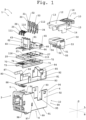
- FIG. 1 An electrical connector 1 is shown, which is designed as a socket 2.
- the socket 2 has a housing 10, wherein the housing 10 can be divided into an upper housing part 90 and a lower housing part 12. Both the lower housing part 12 and the upper housing part 90 are made of a conductive material, in particular of a metal housing 10. This ensures the electromagnetic compatibility and reduces electromagnetic interference.
- the metal housing 10 can be formed, for example, from sheet metal or a die-cast metal part, in particular a zinc die-cast part.
- the lower housing part 12 has a front side 3 and a rear side 4, wherein the front side 3 is the side into which a complementary plug is inserted and the rear side 4 is the side into which a cable (not shown) is inserted into the socket 2.
- the front side 3 has a window for this purpose, which has the typical shape of an RJ45 plug.
- the lower housing part 90 has a base 91 and, starting from the base 91, two side surfaces 92 pointing towards the upper housing part 11. The base 91 and the two side surfaces 92 connect the front side 3 and the rear side 4 to one another.
- the rear side 4 has an open surface 93.
- the lower housing part 90 has a roof 94.
- the roof 94 runs parallel to the base 91.
- the spatial plane in which the base 91 of the lower housing part 90 is arranged is defined as the underside 6 of the socket 2.
- the spatial plane in which the roof 94 is arranged is defined as the top side 5 of the socket 2.
- Each side surface 92 has an L-shaped bulge 95.
- the side surface 92 has holding means, which are preferably designed as bulges 96-98. A total of three bulges 96-98 are formed on each side surface 92.
- the first bulge 96 is arranged in the area of the rear side 4 and top side 5.
- the second bulge 97 is arranged in the middle of the side surface 92 and the third bulge 98 is arranged in the central region near the front side 3.
- a shielding part 80 is arranged within the lower housing part 90.
- the shielding part 80 has a base plate 81, wherein the base plate 81 rests on the bottom 91 of the lower housing part 90.
- the base plate 81 forms a fastening element 88 on the front edge, which points in the direction of the underside 6 of the socket 2.
- the shielding part 80 is fixed to the lower housing part 90 by the fastening element 88 and by a complementary holding means (not shown) of the lower housing part 90.
- the shielding part 80 Near the rear side 4, the shielding part 80 has two first outer surfaces 82, wherein the first outer surfaces 82 run parallel to the side surfaces 92 of the lower housing part 90.
- the two first outer surfaces 82 are connected to one another in the region of the upper side 5 via an overhang 84.
- the overhang 84 has an arcuate shape, with the arcuate shape of the overhang 84 decreasing towards the interior of the socket 2.
- the overhang 84 is arranged closer to the rear side 4 than the loading piece 50.
- the roof also has a fixing element 16 which projects beyond the rear side 4 of the socket 2. Using a cable tie (not shown) and the fixing element 16, the cable to be inserted can be additionally mechanically fixed to the socket 2.
- first outer surfaces 82 have holding means in the form of first locking lugs 85.
- the first locking lugs 85 point towards the interior of the socket 2.
- two L-shaped second outer surfaces 83 are arranged.
- the second outer surfaces 83 run parallel to the side surfaces 92 of the housing base 90.
- At the free end of the L-shaped A retaining lug 87 is arranged on the second outer surface 83, which points in the direction of the side surfaces 92 of the lower housing part 90. In the assembled state, the retaining lug 87 engages in the third bulge 98 of the lower housing part 90.
- the L-shaped second outer surfaces 83 are pressed in the direction of the side surfaces 92 of the lower housing part 90, whereby the retaining lugs 87 are pressed more firmly into the third bulge 98 of the lower housing part 90.
- the shielding part 80 and the shielding of the connector make contact, among other things, via the L-shaped second outer surfaces 83.
- the shielding transfer from the socket 2 to the connector takes place in this area.
- the second outer surfaces 83 have holding means in the form of second locking lugs 86.
- the second locking lugs 86 point in the direction of the interior of the socket 2.
- the upper housing part 11 is U-shaped. It has a roof 12, which is arranged in the space in the upper side 5 of the socket 2.
- the roof 12 has a canopy 13, which, when assembled, nestles into a protrusion 99 of the roof 94 of the lower housing part 90.
- the upper housing part 11 has a side wall 14, wherein a portion of the side wall 14 is L-shaped and nestles into the L-shaped bulge 95 of the side surface 92 of the lower housing part 90 when assembled.
- the region of the side wall 14 that is arranged closer to the rear side 4 is indented towards the center of the socket 2 and has a retaining means, which is preferably designed as a nose 15.
- the upper housing part 11 can be connected to the lower housing part 90 by means of a snap-fit connection.
- the nose 15 of the upper housing part 11 engages in the first bulge 96 of the lower housing part 90.
- a charging piece 50 is arranged in the upper housing part 11, wherein the charging piece 50 is made of a non-electrically conductive material, in particular of plastic.
- the body of the charging piece 50 is L-shaped.
- the first leg 51 of the L-shaped body which runs parallel to the top side 5 of the socket 2, preferably has four through-holes 52 through which the individual wires of the cable to be inserted are passed.
- guides 54 are arranged in the first leg 51, through which a row of insulation displacement terminals 31 can be passed.
- the second leg 53 of the L-shaped body stands perpendicular to the top side 5 of the socket 2 and has cavities 55.
- First contact elements 30, which are preferably designed as insulation displacement terminals 31, can be inserted through the guides 54 of the first leg 51 and the recesses 55 of the second leg 52.
- the insulation displacement terminals 31 penetrate the guides 54 or recesses 55, thereby stripping the individual wires of the inserted cable and establishing an electrical connection.
- the insulation displacement terminals 31 are arranged near the rear side 4.
- the insulation displacement terminals 31 point towards the upper housing part 11.
- the insulation displacement terminal 31 has a foot 110, which can be passed through a first through-opening 115.
- the foot 110 of the insulation displacement terminal 31 is electrically and mechanically contacted by means of soldering or pressing with the first contact pad 117.
- the insulation displacement terminal 31 has a hole 34 in its center.
- the insulation displacement terminals 31 are arranged in two rows, wherein a row is characterized in that the feet 110 of the insulation displacement terminals 31 in one row are arranged at the same distance from the rear side 4 of the connector.
- the insulation displacement terminals 31 can be arranged in one row or in more than one row, for example in two, three, four, or five rows.
- the insulation displacement terminal surfaces 32 are aligned parallel to one another in the present case.
- the insulation displacement terminal surfaces 32 of different rows can be at an angle to one another.
- the insulation displacement terminal surfaces 32 of insulation displacement terminals 31 in one row can be at different angles to one another.
- the insulation displacement terminal surfaces 32 can be perpendicular to one another.
- the insulation displacement terminals 31 in one row can have a different height than the insulation displacement terminals 31 in another row, with the height of an insulation displacement terminal 31 being the distance between the point on the insulation displacement terminal 31 into which a cable can be inserted and the top of the circuit board.
- the insulation displacement terminals 31 within a row can have different heights from one another. This makes it possible to design the socket 2 more compactly, since the installation space is optimized by arranging the individual wires one above the other in the charging piece 50.
- Each insulation displacement terminal 31 is electrically connected to a second contact element 35, which is preferably designed as a plug contact 36, via a conductor track 21.
- the plug contacts 36 are arranged near the front side 3 of the socket 2.
- the plug contacts 36 have a foot 111 which fits into a second through-opening 116 on the
- the printed circuit board 20 is guided and is mechanically fixed and electrically contacted by means of pressing and/or soldering.
- the plug contacts 36 are pin-shaped, with the plug contacts 36 projecting upwards toward the rear side 4 of the socket 2.
- the plug contacts 36 connected to conductor tracks three 103 and six 106 are shorter than the other plug contacts 36.
- the plug contacts 36 are spring-loaded.
- a support element 60 Arranged above the circuit board 20 is a support element 60 having recesses 61 through which the insulation displacement terminals 31 are guided.
- a raised portion 62 is formed, which, when assembled, touches the roof 12 of the upper housing part 11.
- a first notch 64 is arranged on the outer surface 63 of the raised portion 62, into which the second locking lug 86 of the shielding part 80 engages.
- a further second notch 65 is formed, into which the first locking lug 85 of the shielding part 80 engages. The engagement of the two locking lugs 85, 86 mechanically fixes the support element 60 to the shielding part 80.
- the carrier element 60 has, in the region of the rear side 4 on its lower side, two pins 66 which can be inserted into two complementary holes 27 on the printed circuit board 20 and two indentations 72 in the cover 70 and prevent displacement along a plane.
- the cover 70 is arranged below the circuit board 20.
- the cover 70 has rails 73 that rest on the base plate 81 of the shielding part 80. Furthermore, the cover 70 has recesses 71, 74 into which the feet 110, 111 of the plug contacts 36 and the insulation displacement terminals 31, which extend through the circuit board 20, can penetrate.
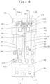
- the printed circuit board 20 is depicted with plug contacts 36 and insulation displacement terminals 31 arranged thereon.
- the plug contacts 36 are arranged in two rows, with the number of plug contacts 36 varying within a row.
- the row arranged closer to the front 3 of the socket 2 has six plug contacts 36, whereas the row arranged further from the front 3 of the socket 2 has two plug contacts 36.
- the number of rows and the number of plug contacts 36 within a row are variable.
- the plug contacts 36 in the second row are shorter than the other plug contacts 36.
- the plug contacts 36 can reach different heights with respect to the printed circuit board 20 and can protrude different distances towards the center of the circuit board.
- each conductor track 21 connects an insulation displacement terminal 31 to a plug contact 36.
- a conductor track 21 has a first contact pad 117 and a second contact pad 118, which are arranged around a first through-opening 115 and a second through-opening 116 and are electrically connected via a conductor path 25.
- the conductor path 25 can run over different circuit board layers 26 and have different conductor track widths. It has proven advantageous that, starting from the insulation displacement terminal 31, the width of the conductor track 21 becomes increasingly smaller and the distance between the conductor tracks 21, for example of a differential line 22, increases. This is advantageous because the impedance of the insulation displacement terminal 31 is significantly greater than the Impedance of the plug contact 36 and with a step-by-step adjustment of the impedance of the line path 25, the insertion loss and return loss are significantly improved.
- the circuit board 20 has eight conductor tracks 21.
- Two conductor tracks 21 each form a differential line 22, whereby a distinction is made between the first conductor track 23 and the second conductor track 24 for the two conductor tracks 21 of a differential line 22.
- four first conductor tracks 23 and four second conductor tracks 24 are arranged on the circuit board 20.
- the four first conductor tracks 23 are defined as conductor track one 101, conductor track three 103, conductor track five 105, and conductor track seven 107
- the second conductor tracks 24 are defined as conductor track two 102, conductor track four 104, conductor track six 106, and conductor track eight 108.
- Conductor track one 101 and conductor track two 102 form a first differential line 121.
- Conductor track three 103 and conductor track six 106 form a second differential line 122.
- Conductor track four 104 and conductor track five 105 form a third differential line 123, and conductor track seven 107 and conductor track eight 108 form a fourth differential line 124.
- the conductor tracks 21 of a differential line 22 can run on different circuit board layers 26, with the individual sections of the conductor tracks on the different circuit board layers 26 usually being connected by means of vias 29.
- the circuit board 20 has a total of nine compensation units 125, wherein the compensation units 125 are configured as plate capacitors 126.
- a plate capacitor 126 has two conductive plates 127 running parallel to one another. A dielectric is arranged between the plates 127.
- the capacitance of the plate capacitor 126 can be varied by selecting the circuit board layers 26 on which the plates 127 of the plate capacitor 126 are arranged. The capacitance can also be varied by changing the surface area of the plates 127 of the plate capacitor 126.
- the plates 127 of the plate capacitors 126 are preferably square and arranged almost completely overlapping one another. However, the plates 127 can also be polygonal, round, or oval.
- the plates 127 of the plate capacitors 126 are connected, for example, to a conductor track 21 via stub lines 28.
- the stub line 28 can be connected to a contact pad 117, 118 or the conductor path 25.
- Two of the nine plate capacitors 126 are connected between conductor track one 101 and conductor track three 103, with one plate capacitor 126 located near the insulation displacement terminals 31 and the other plate capacitor 126 located near the plug contacts 36. Another plate capacitor 126 is connected between conductor track six 106 and conductor track eight 108. Another plate capacitor 126 is connected between conductor track four 104 and conductor track six 106. Another plate capacitor 126 is connected between conductor track three 103 and conductor track five 105. Another plate capacitor 126 is connected between conductor track five 105 and conductor track six 106. Another plate capacitor 126 is connected between conductor track two 102 and conductor track four 104. Another plate capacitor 126 is connected between the conductor track four 104 and the conductor track eight 108. Another Plate capacitor 126 is connected between conductor track three 103 and conductor track seven 107. The plate capacitors 126 can also be designed as interdigital capacitors.
- the conductive surfaces 40 are formed in the inner circuit board layers 26. However, conductive surfaces 40 can also be arranged in the uppermost circuit board layer 26 and in the lowermost circuit board layer 26. A total of forty-six conductive surfaces 40 are arranged on the circuit board 20. However, more or fewer conductive surfaces 40 can also be arranged on the circuit board 20. Furthermore, a different number of conductive surfaces 40 can be arranged on the individual circuit board layers 26, in particular on the inner circuit board layers 26. The number of conductive surfaces 40 is selected such that the conductive surfaces 40 are preferably not arranged overlapping a conductive surface of the circuit, in particular the signal paths.
- the signal path is defined as the path which transmits a signal through the socket 2 on a direct path.
- the conductive surface 40 can be arranged overlapping a conductor track 21, in particular a signal path. However, the conductive surface 40 should not be arranged to overlap more than one signal path, since the influence on the impedance and thus on the insertion loss and return loss, as well as on the compensation circuit, would be too great and a change in the circuit design would be necessary to ensure the same transmission performance and comply with the standard requirements.
- Several conductive surfaces 40 can overlap a conductive path 25 or a contact pad 117, 118.
- a conductive surface 40 does not overlap two conductive paths 25 or two contact pads 117, 118, or a conductive path 25 and a contact pad 117, 118.
- the conductive surfaces 40 have no influence at all or no measurable influence on the conductive surfaces on the Printed circuit board 20, this is achieved in particular by the fact that no conductive surface 40 is arranged below or above a conductive path 25 or contact pads 117, 118.
- the conductive surfaces 40 can be arranged overlapping the compensation units 125, which are preferably designed as plate capacitors 126. The influence of the conductive surfaces 40 on the capacitances of the plate capacitors 126 is usually negligible. Likewise, one conductive surface 40 or several conductive surfaces 40 can be arranged overlapping to form a stub line 28. It is irrelevant whether the stub line 28 is connected to a contact pad 117, 118 or to a conduction path 25.
- the conductive surfaces 40 are designed such that they are small enough to overlap one or no conductor tracks 21, yet large enough to provide stability to the layer structure. Furthermore, as much of a printed circuit board layer 26 as possible should be covered with conductive surfaces 40. A minimum distance from the edge of the printed circuit board layer 26 is preferably maintained. However, the conductive surfaces 40 can also be arranged directly at the edge of a printed circuit board layer 26.
- the conductive surfaces 40 are preferably arranged in rows 41 on the circuit board 20, but can also be arranged individually on the circuit board 20.
- a row 41 has at least two conductive surfaces 40, wherein the conductive surface centers 43 of the conductive surfaces 40 of a row 41 lie on an imaginary line, wherein the line is arranged parallel to the longitudinal axis L or to the width axis B.
- the longitudinal axis L is orthogonal to the width axis B and the transverse axis Q.
- a conductive surface 40 can be part of two or more rows 41.
- the circuit board 20 has thirty-two Rows 41, with each circuit board layer 26 forming sixteen rows 41.
- each circuit board layer 26 four rows 41 with three conductive surfaces 40, eleven rows 41 with two conductive surfaces 40, and one row 41 with five conductive surfaces 40 are formed. Ten rows 41 are formed on an imaginary line arranged parallel to the longitudinal axis L, and six rows 41 are formed on an imaginary line arranged parallel to the width axis B.
- the arrangement of the conductive surfaces 40 gives the circuit board layer structure even more stability.
- the conductive surfaces 40 can also be arranged offset from one another, whereby areas that are critical with regard to the stability of the layer structure are specifically reinforced.
- the arrangement of conductive surfaces 40 can be arranged in groups. At least one group 42 can be arranged on the circuit board 20.
- a group 42 has at least two overlapping, preferably completely overlapping, rows 41.
- a group 42 does not have to use every member of a row 41 to be considered a group 42. However, at least two members of a row 41 must be involved in forming a group 42.
- the members of group 42 do not have to be adjacent to one another.
- the topmost circuit board layer 26 is indicated by solid lines, and the underlying circuit board layers 26 are indicated by dashed lines.
- the compensation units 125 are clearly visible, with the plates 127 of most of the plate capacitors 126 arranged completely overlapping each other.
- the two holes 27 are arranged, through which the pins 66 of the carrier element 60 are guided, thus preventing displacement of the circuit board 20. within a plane.
- the second contact pads 118 are significantly smaller than the first contact pads 117. Both contact pads 117, 118 are oval-shaped.
- Conductor tracks one 101 and two 102 of the first differential line 121 are arranged to completely overlap one another in sections. The same applies to the fourth differential line 124.
- conductor tracks five 105 and six 106 run over one another in sections, as do conductor tracks three 103 and four 104.
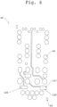
- the inner circuit board layers 26 are shown.
- the conductive surfaces 40 are clearly visible.
- the conductive surfaces 40 can be round as shown, but also oval or polygonal, in particular square, or have the shape of a parallelogram or a trapezoid.
- the conductive surfaces 40 are designed such that as many conductive surfaces as possible and as large as possible can be arranged on the circuit board 20. To achieve this, the conductive surfaces 40 must adapt to the circuit design and adjust their shape accordingly.
- the plates 127 of a plate capacitor 126 are never arranged on adjacent inner circuit board layers 26.
- the plates 127 of a plate capacitor 126 can also be arranged on adjacent inner circuit board layers 26.
Landscapes
- Physics & Mathematics (AREA)
- Electromagnetism (AREA)
- Engineering & Computer Science (AREA)
- Microelectronics & Electronic Packaging (AREA)
- Details Of Connecting Devices For Male And Female Coupling (AREA)
Applications Claiming Priority (1)
| Application Number | Priority Date | Filing Date | Title |
|---|---|---|---|
| DE102023125696.3A DE102023125696B4 (de) | 2023-09-21 | 2023-09-21 | Elektrischer Verbinder für ein Datenkabel |
Publications (1)
| Publication Number | Publication Date |
|---|---|
| EP4529366A1 true EP4529366A1 (fr) | 2025-03-26 |
Family
ID=91960422
Family Applications (1)
| Application Number | Title | Priority Date | Filing Date |
|---|---|---|---|
| EP24189851.9A Pending EP4529366A1 (fr) | 2023-09-21 | 2024-07-19 | Connecteur électrique pour câble de données |
Country Status (2)
| Country | Link |
|---|---|
| EP (1) | EP4529366A1 (fr) |
| DE (1) | DE102023125696B4 (fr) |
Citations (4)
| Publication number | Priority date | Publication date | Assignee | Title |
|---|---|---|---|---|
| US7345889B1 (en) * | 2004-09-28 | 2008-03-18 | Avaya Technology Corp. | Method and system for reducing radiated energy emissions in computational devices |
| WO2014158987A1 (fr) * | 2013-03-14 | 2014-10-02 | Boulder Wind Power, Inc. | Procédés et appareils pour optimiser des zones inopérantes électriquement sur des ensembles composites stratifiés |
| US8915756B2 (en) | 2013-01-23 | 2014-12-23 | Commscope, Inc. Of North Carolina | Communication connector having a printed circuit board with thin conductive layers |
| US20150228706A1 (en) * | 2014-02-10 | 2015-08-13 | Samsung Display Co., Ltd. | Display device |
Family Cites Families (1)
| Publication number | Priority date | Publication date | Assignee | Title |
|---|---|---|---|---|
| DE102008026467B4 (de) * | 2008-06-03 | 2011-12-29 | Mc Technology Gmbh | Steckverbindersystem |
-
2023
- 2023-09-21 DE DE102023125696.3A patent/DE102023125696B4/de active Active
-
2024
- 2024-07-19 EP EP24189851.9A patent/EP4529366A1/fr active Pending
Patent Citations (4)
| Publication number | Priority date | Publication date | Assignee | Title |
|---|---|---|---|---|
| US7345889B1 (en) * | 2004-09-28 | 2008-03-18 | Avaya Technology Corp. | Method and system for reducing radiated energy emissions in computational devices |
| US8915756B2 (en) | 2013-01-23 | 2014-12-23 | Commscope, Inc. Of North Carolina | Communication connector having a printed circuit board with thin conductive layers |
| WO2014158987A1 (fr) * | 2013-03-14 | 2014-10-02 | Boulder Wind Power, Inc. | Procédés et appareils pour optimiser des zones inopérantes électriquement sur des ensembles composites stratifiés |
| US20150228706A1 (en) * | 2014-02-10 | 2015-08-13 | Samsung Display Co., Ltd. | Display device |
Also Published As
| Publication number | Publication date |
|---|---|
| DE102023125696B4 (de) | 2025-04-03 |
| DE102023125696A1 (de) | 2025-03-27 |
Similar Documents
| Publication | Publication Date | Title |
|---|---|---|
| DE69112658T2 (de) | Abgeschirmter Verbinder. | |
| DE3752310T2 (de) | Elektrische Steckverbinder | |
| DE69619429T2 (de) | Hochleistungsfähiger Leiterplattenrandverbinder | |
| DE3909263C2 (fr) | ||
| DE60032954T2 (de) | Hochgeschwindigkeitsstecker und Verbindung für Leiterplatte | |
| DE60129508T2 (de) | Kommunikationsverbinder mit Nebensprechkompensation | |
| DE60036250T2 (de) | Modularer Jack-Verbinder mit Filtereinsatz und Kontakt dafür | |
| DE69931430T2 (de) | Modularer Verbinder für hohe Übertragungsgeschwindigkeiten | |
| DE2205265A1 (de) | Verbinder | |
| EP0921609A2 (fr) | Connecteur coaxial à haute fréquence et à angle droit | |
| EP2979333B1 (fr) | Connecteur à compensation de diaphonie | |
| EP1535372B1 (fr) | Fiche femelle electrique | |
| EP3435482B1 (fr) | Liaison de connexion comprenant un système de câble et un système de plaque, procédé de fabrication d'une telle liaison de connexion | |
| DE102025121790A1 (de) | Hochleistungsfähige platine zu platine verbinder | |
| DE3883626T2 (de) | Vielfache Verbindungsvorrichtung. | |
| DE4236945A1 (de) | Verbindungselement für eine Hochfrequenz-Signalübertragungsstrecke | |
| DE3525012A1 (de) | Busleiste fuer die oberflaechenmontage | |
| DE69927662T2 (de) | Verbinder zum Abschliessen von Fernmeldekabeln | |
| DE102023125696B4 (de) | Elektrischer Verbinder für ein Datenkabel | |
| DE4126172A1 (de) | Stecker fuer koaxialbandkabel | |
| WO2012171565A1 (fr) | Système de contact électrique servant à relier des circuits imprimés | |
| DE10322172B4 (de) | Kontaktleiste zur elektrischen Kontaktierung von beidseitig auf einer Leiterplatte verlaufenden metallischen Leiterbahnen | |
| AT520584B1 (de) | RJ-45 Stecker für Hochfrequenzanwendungen | |
| EP1160921B1 (fr) | Connecteur pour connecter des fils à une carte à circuits | |
| DE102023121768B3 (de) | Elektrischer Verbinder für ein Daten- oder Kommunikationska-bel |
Legal Events
| Date | Code | Title | Description |
|---|---|---|---|
| PUAI | Public reference made under article 153(3) epc to a published international application that has entered the european phase |
Free format text: ORIGINAL CODE: 0009012 |
|
| STAA | Information on the status of an ep patent application or granted ep patent |
Free format text: STATUS: THE APPLICATION HAS BEEN PUBLISHED |
|
| AK | Designated contracting states |
Kind code of ref document: A1 Designated state(s): AL AT BE BG CH CY CZ DE DK EE ES FI FR GB GR HR HU IE IS IT LI LT LU LV MC ME MK MT NL NO PL PT RO RS SE SI SK SM TR |
|
| STAA | Information on the status of an ep patent application or granted ep patent |
Free format text: STATUS: REQUEST FOR EXAMINATION WAS MADE |
|
| 17P | Request for examination filed |
Effective date: 20250926 |