EP4531415A1 - Verfahren und vorrichtung zur bestimmung von pixeldaten und elektronische vorrichtung - Google Patents
Verfahren und vorrichtung zur bestimmung von pixeldaten und elektronische vorrichtung Download PDFInfo
- Publication number
- EP4531415A1 EP4531415A1 EP23893128.1A EP23893128A EP4531415A1 EP 4531415 A1 EP4531415 A1 EP 4531415A1 EP 23893128 A EP23893128 A EP 23893128A EP 4531415 A1 EP4531415 A1 EP 4531415A1
- Authority
- EP
- European Patent Office
- Prior art keywords
- pixel data
- photosensitive
- scan sensor
- line scan
- row
- Prior art date
- Legal status (The legal status is an assumption and is not a legal conclusion. Google has not performed a legal analysis and makes no representation as to the accuracy of the status listed.)
- Pending
Links
Images


Classifications
-
- H—ELECTRICITY
- H04—ELECTRIC COMMUNICATION TECHNIQUE
- H04N—PICTORIAL COMMUNICATION, e.g. TELEVISION
- H04N25/00—Circuitry of solid-state image sensors [SSIS]; Control thereof
- H04N25/60—Noise processing, e.g. detecting, correcting, reducing or removing noise
- H04N25/61—Noise processing, e.g. detecting, correcting, reducing or removing noise the noise originating only from the lens unit, e.g. flare, shading, vignetting or "cos4"
- H04N25/611—Correction of chromatic aberration
-
- H—ELECTRICITY
- H04—ELECTRIC COMMUNICATION TECHNIQUE
- H04N—PICTORIAL COMMUNICATION, e.g. TELEVISION
- H04N25/00—Circuitry of solid-state image sensors [SSIS]; Control thereof
- H04N25/70—SSIS architectures; Circuits associated therewith
- H04N25/701—Line sensors
-
- H—ELECTRICITY
- H04—ELECTRIC COMMUNICATION TECHNIQUE
- H04N—PICTORIAL COMMUNICATION, e.g. TELEVISION
- H04N1/00—Scanning, transmission or reproduction of documents or the like, e.g. facsimile transmission; Details thereof
- H04N1/04—Scanning arrangements, i.e. arrangements for the displacement of active reading or reproducing elements relative to the original or reproducing medium, or vice versa
- H04N1/19—Scanning arrangements, i.e. arrangements for the displacement of active reading or reproducing elements relative to the original or reproducing medium, or vice versa using multi-element arrays
- H04N1/191—Scanning arrangements, i.e. arrangements for the displacement of active reading or reproducing elements relative to the original or reproducing medium, or vice versa using multi-element arrays the array comprising a one-dimensional [1D] array
- H04N1/192—Simultaneously or substantially simultaneously scanning picture elements on one main scanning line
- H04N1/193—Simultaneously or substantially simultaneously scanning picture elements on one main scanning line using electrically scanned linear arrays, e.g. linear CCD arrays
-
- H—ELECTRICITY
- H04—ELECTRIC COMMUNICATION TECHNIQUE
- H04N—PICTORIAL COMMUNICATION, e.g. TELEVISION
- H04N1/00—Scanning, transmission or reproduction of documents or the like, e.g. facsimile transmission; Details thereof
- H04N1/04—Scanning arrangements, i.e. arrangements for the displacement of active reading or reproducing elements relative to the original or reproducing medium, or vice versa
- H04N1/19—Scanning arrangements, i.e. arrangements for the displacement of active reading or reproducing elements relative to the original or reproducing medium, or vice versa using multi-element arrays
- H04N1/191—Scanning arrangements, i.e. arrangements for the displacement of active reading or reproducing elements relative to the original or reproducing medium, or vice versa using multi-element arrays the array comprising a one-dimensional [1D] array
- H04N1/192—Simultaneously or substantially simultaneously scanning picture elements on one main scanning line
- H04N1/193—Simultaneously or substantially simultaneously scanning picture elements on one main scanning line using electrically scanned linear arrays, e.g. linear CCD arrays
- H04N1/1934—Combination of arrays
-
- H—ELECTRICITY
- H04—ELECTRIC COMMUNICATION TECHNIQUE
- H04N—PICTORIAL COMMUNICATION, e.g. TELEVISION
- H04N1/00—Scanning, transmission or reproduction of documents or the like, e.g. facsimile transmission; Details thereof
- H04N1/46—Colour picture communication systems
- H04N1/48—Picture signal generators
- H04N1/486—Picture signal generators with separate detectors, each detector being used for one specific colour component
-
- H—ELECTRICITY
- H04—ELECTRIC COMMUNICATION TECHNIQUE
- H04N—PICTORIAL COMMUNICATION, e.g. TELEVISION
- H04N23/00—Cameras or camera modules comprising electronic image sensors; Control thereof
- H04N23/10—Cameras or camera modules comprising electronic image sensors; Control thereof for generating image signals from different wavelengths
- H04N23/13—Cameras or camera modules comprising electronic image sensors; Control thereof for generating image signals from different wavelengths with multiple sensors
- H04N23/15—Image signal generation with circuitry for avoiding or correcting image misregistration
-
- H—ELECTRICITY
- H04—ELECTRIC COMMUNICATION TECHNIQUE
- H04N—PICTORIAL COMMUNICATION, e.g. TELEVISION
- H04N23/00—Cameras or camera modules comprising electronic image sensors; Control thereof
- H04N23/80—Camera processing pipelines; Components thereof
- H04N23/84—Camera processing pipelines; Components thereof for processing colour signals
-
- H—ELECTRICITY
- H04—ELECTRIC COMMUNICATION TECHNIQUE
- H04N—PICTORIAL COMMUNICATION, e.g. TELEVISION
- H04N23/00—Cameras or camera modules comprising electronic image sensors; Control thereof
- H04N23/80—Camera processing pipelines; Components thereof
- H04N23/84—Camera processing pipelines; Components thereof for processing colour signals
- H04N23/843—Demosaicing, e.g. interpolating colour pixel values
-
- H—ELECTRICITY
- H04—ELECTRIC COMMUNICATION TECHNIQUE
- H04N—PICTORIAL COMMUNICATION, e.g. TELEVISION
- H04N25/00—Circuitry of solid-state image sensors [SSIS]; Control thereof
- H04N25/10—Circuitry of solid-state image sensors [SSIS]; Control thereof for transforming different wavelengths into image signals
-
- H—ELECTRICITY
- H04—ELECTRIC COMMUNICATION TECHNIQUE
- H04N—PICTORIAL COMMUNICATION, e.g. TELEVISION
- H04N25/00—Circuitry of solid-state image sensors [SSIS]; Control thereof
- H04N25/10—Circuitry of solid-state image sensors [SSIS]; Control thereof for transforming different wavelengths into image signals
- H04N25/11—Arrangement of colour filter arrays [CFA]; Filter mosaics
-
- H—ELECTRICITY
- H04—ELECTRIC COMMUNICATION TECHNIQUE
- H04N—PICTORIAL COMMUNICATION, e.g. TELEVISION
- H04N25/00—Circuitry of solid-state image sensors [SSIS]; Control thereof
- H04N25/40—Extracting pixel data from image sensors by controlling scanning circuits, e.g. by modifying the number of pixels sampled or to be sampled
-
- H—ELECTRICITY
- H04—ELECTRIC COMMUNICATION TECHNIQUE
- H04N—PICTORIAL COMMUNICATION, e.g. TELEVISION
- H04N25/00—Circuitry of solid-state image sensors [SSIS]; Control thereof
- H04N25/70—SSIS architectures; Circuits associated therewith
- H04N25/703—SSIS architectures incorporating pixels for producing signals other than image signals
- H04N25/708—Pixels for edge detection
Definitions
- the present disclosure relates to the field of image processing, and specifically, to a pixel data determination method and apparatus, and an electronic device.
- the line array sensor performs linear scanning, and has the advantages of a wide coverage, a compact structure, a space-saving design, 1:1 image reproduction without distortion, etc.
- This type of line array camera is a line scan camera formed by three rows of red, green, and blue chips. Each pixel point comprises red, green, and blue pixel data. In the scanning process, each pixel point is exposed multiple times, and with the combination of the red, green, and blue photosensitive chips, a color image can be formed with only a single white light illumination.
- using the method to determine the color image can easily result in the occurrence of a color edge in the determined image, which may interfere with the final image determination and recognition.
- Embodiments of the present disclosure provide a pixel data determination method and apparatus, and an electronic device, so as to at least solve the technical problems that in the related art, when determining target pixel data corresponding to a target pixel row, the target pixel data may exhibit a color edge.
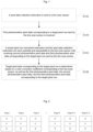
- a pixel data determination method includes: sending a pixel data collection instruction to a line scan sensor, where the line scan sensor includes three photosensitive chips arranged in parallel, the three photosensitive chips respectively correspond to three colors, and the pixel data collection instruction is configured to enable the three photosensitive chips located at different positions to respectively scan corresponding pixel rows; receiving first photosensitive pixel data corresponding to a target pixel row sent by the line scan sensor, where the first photosensitive pixel data is photosensitive pixel data scanned by a first position photosensitive chip, and when the first photosensitive pixel data corresponding to the target pixel row is acquired, the target pixel row corresponds to a scanning position of the first position photosensitive chip; cyclically and sequentially sending a preset pixel row movement instruction and the pixel data collection instruction to the line scan sensor until receiving second photosensitive pixel data and third photosensitive pixel data corresponding to the target pixel row sent by the line scan sensor, where the second photosensitive pixel data is photosensitive pixel data
- the method before the sending a pixel data collection instruction to a line scan sensor, the method further includes: acquiring a scanning area where the line scan sensor scans an object to be scanned; determining an initial scanning position of the scan sensor based on the scanning area; and sending a position adjustment instruction to the line scan sensor, where the position adjustment instruction carries the initial scanning position.
- the method further includes: determining an end scanning position of the scan sensor based on the scanning area; determining all pixel rows from the initial scanning position to the end scanning position; cyclically and sequentially sending the preset pixel row movement instruction and the pixel data collection instruction to the line scan sensor until receiving the first photosensitive pixel data, the second photosensitive pixel data, and the third photosensitive pixel data respectively corresponding to all the pixel rows sent by the line scan sensor; and determining image data corresponding to the scanning area based on the first photosensitive pixel data, the second photosensitive pixel data, and the third photosensitive pixel data respectively corresponding to all the pixel rows.
- the method before the sending a pixel data collection instruction to a line scan sensor, the method further includes: determining a moving pixel row; and determining the pixel data collection instruction and the preset pixel row movement instruction based on the moving pixel row.
- the determining a moving pixel row includes: acquiring a target resolution; and determining the target moving pixel row based on the target resolution.
- the method before the determining target pixel data corresponding to the target pixel row based on a color correction coefficient corresponding to the line scan sensor, as well as the first photosensitive pixel data, the second photosensitive pixel data, and the third photosensitive pixel data corresponding to the target pixel row, the method includes: acquiring the color correction coefficient corresponding to the line scan sensor.
- the three photosensitive chips include: a blue light photosensitive chip, a green light photosensitive chip, and a red light photosensitive chip.
- a pixel data determination apparatus includes: a sending module, configured to send a pixel data collection instruction to a line scan sensor, where the line scan sensor includes three photosensitive chips located at different positions, and the pixel data collection instruction is configured to enable the three photosensitive chips located at the different positions to respectively scan corresponding pixel rows; a receiving module, configured to receive first photosensitive pixel data corresponding to a target pixel row sent by the line scan sensor, where the first photosensitive pixel data is photosensitive pixel data scanned by a first position photosensitive chip, and when the first photosensitive pixel data corresponding to the target pixel row is acquired, the target pixel row corresponds to a scanning position of the first position photosensitive chip; a transceiving module, configured to cyclically and sequentially send a preset pixel row movement instruction and the pixel data collection instruction to the line scan sensor until receiving second photosensitive pixel data and third photosensitive pixel data corresponding to the target pixel row sent by the line scan sensor,
- an electronic device includes a processor; and a memory configured to store executable instructions of the processor, where the processor is configured to execute the instructions to implement any one of the above pixel data determination methods.
- a computer-readable storage medium is provided. Instructions in the computer-readable storage medium, when executed by a processor of an electronic device, cause the electronic device to perform any one of the above pixel data determination methods.
- the pixel data collection instruction is sent to the line scan sensor, where the line scan sensor includes the three photosensitive chips arranged in parallel, the three photosensitive chips respectively correspond to three colors, and the pixel data collection instruction is configured to enable the three photosensitive chips located at the different positions to respectively scan the corresponding pixel rows.
- the first photosensitive pixel data corresponding to the target pixel row sent by the line scan sensor is received.
- the preset pixel row movement instruction and the pixel data collection instruction are cyclically and sequentially sent to the line scan sensor until receiving the second photosensitive pixel data and the third photosensitive pixel data corresponding to the target pixel row sent by the line scan sensor, where the first photosensitive pixel data is photosensitive pixel data scanned by the first position photosensitive chip, and when the first photosensitive pixel data corresponding to the target pixel row is acquired, the target pixel row corresponds to the scanning position of the first position photosensitive chip; the second photosensitive pixel data is the photosensitive pixel data scanned by the second position photosensitive chip, and the third photosensitive pixel data is the photosensitive pixel data scanned by the third position photosensitive chip; when the second photosensitive pixel data corresponding to the target pixel row is acquired, the target pixel row corresponds to the scanning position of the second position photosensitive chip; and when the third photosensitive pixel data corresponding to the target pixel row is acquired, the target pixel row corresponds to the scanning position of the third position photosensitive chip.
- the target pixel data corresponding to the target pixel row is determined based on the color correction coefficient corresponding to the line scan sensor, as well as the first photosensitive pixel data, the second photosensitive pixel data, and the third photosensitive pixel data corresponding to the target pixel row. That is, the pixel data of the target pixel row is determined through multi-time scanning based on the respective scanning of the first position photosensitive chip, the second position photosensitive chip, and the third position photosensitive chip, and is obtained through scanning at the determined scanning positions. Compared with the related art, pixel data of a target pixel row is obtained through one-time scanning that scans all pixel data, and after correction through the color correction coefficient, the problem of color fringing may exist.
- the corresponding pixel data is scanned at the determined scanning positions, such that an area range of the determined pixel data is standard.
- the determined pixel data is more accurate, meaning that the problem of color fringing cannot occur, thereby solving the technical problem that in the related art, when the target pixel data corresponding to the target pixel row is determined, the target pixel data may exhibit a color edge.
- a process, a method, a system, a product, or a device including a series of steps or units is not necessarily limited to those explicitly-listed steps or units, but may include other steps or units that are not explicitly listed or inherent to the process, the method, the system, the product, or the device.
- an embodiment of a pixel data determination method is provided. It should be noted that steps shown in the flowchart of the accompanying drawings may be performed in a computer system, such as a set of computer-executable instructions. Furthermore, although a logical sequence is shown in the flowchart, in some cases, the steps shown or described may be performed in a different sequence than that presented herein.
- the method according to the above embodiments may be implemented by software and a necessary general-purpose hardware platform, and certainly, may also be implemented by hardware, but the former is a preferred implementation in many cases.
- the technical solutions of the present disclosure essentially or parts making contribution to the prior art may be embodied in the form of a software product.
- the computer software product is stored in a storage medium (e.g., a ROM/RAM, a magnetic disk, and a compact disc), which includes a plurality of instructions used to allow one terminal device (which may be a mobile phone, a computer, a server, a network device, or the like) to perform the method according to various embodiments of the present disclosure.
- the determination module 608 is connected to the above transceiving module 606, and is configured to determine target pixel data corresponding to the target pixel row based on a color correction coefficient corresponding to the line scan sensor, as well as the first photosensitive pixel data, the second photosensitive pixel data, and the third photosensitive pixel data corresponding to the target pixel row.
- an electronic device includes a processor; and a memory configured to store executable instructions of the processor, where the processor is configured to execute the instructions to implement any one of the above pixel data determination methods.
- the units described as separate components may or may not be physically separated, and components displayed as units may or may not be physical units, that is, may be located in one position, or may be distributed over a plurality of units. Some or all of the units may be selected according to actual needs to achieve the objectives of the solutions of the embodiments.
- various functional units in the embodiments of the present disclosure may be integrated into one processing unit, each of the units may exist alone physically, or two or more units may be integrated into one unit.
- the above integrated unit may be implemented in the form of hardware or a software functional unit.
- the integrated unit may be stored in a computer-readable storage medium.
- the computer software product is stored in a storage medium and includes a plurality of instructions used to allow a computer device (which may be a personal computer, a server, a network device, or the like) to perform all or part of the steps of the methods in the embodiments of the present disclosure.
- the aforementioned storage medium includes a U disk, a read-only memory (ROM), a random access memory (RAM), a mobile hard drive, a magnetic disk, an optical disk, or other media capable of storing program code.
- the pixel data collection instruction is sent to the line scan sensor, where the line scan sensor includes the three photosensitive chips arranged in parallel, the three photosensitive chips respectively correspond to three colors, and the pixel data collection instruction is configured to enable the three photosensitive chips located at the different positions to respectively scan the corresponding pixel rows.
- the first photosensitive pixel data corresponding to the target pixel row sent by the line scan sensor is received.
- the preset pixel row movement instruction and the pixel data collection instruction are cyclically and sequentially sent to the line scan sensor until receiving the second photosensitive pixel data and the third photosensitive pixel data corresponding to the target pixel row sent by the line scan sensor, where the first photosensitive pixel data is photosensitive pixel data scanned by the first position photosensitive chip, and when the first photosensitive pixel data corresponding to the target pixel row is acquired, the target pixel row corresponds to the scanning position of the first position photosensitive chip; the second photosensitive pixel data is the photosensitive pixel data scanned by the second position photosensitive chip, and the third photosensitive pixel data is the photosensitive pixel data scanned by the third position photosensitive chip; when the second photosensitive pixel data corresponding to the target pixel row is acquired, the target pixel row corresponds to the scanning position of the second position photosensitive chip; and when the third photosensitive pixel data corresponding to the target pixel row is acquired, the target pixel row corresponds to the scanning position of the third position photosensitive chip.
Landscapes
- Engineering & Computer Science (AREA)
- Multimedia (AREA)
- Signal Processing (AREA)
- Color Television Image Signal Generators (AREA)
- Image Input (AREA)
- Facsimile Scanning Arrangements (AREA)
- Studio Devices (AREA)
Applications Claiming Priority (2)
| Application Number | Priority Date | Filing Date | Title |
|---|---|---|---|
| CN202211484430.6A CN115866422A (zh) | 2022-11-24 | 2022-11-24 | 像素数据确定方法、装置及电子设备 |
| PCT/CN2023/102899 WO2024109028A1 (zh) | 2022-11-24 | 2023-06-27 | 像素数据确定方法、装置及电子设备 |
Publications (2)
| Publication Number | Publication Date |
|---|---|
| EP4531415A1 true EP4531415A1 (de) | 2025-04-02 |
| EP4531415A4 EP4531415A4 (de) | 2025-12-10 |
Family
ID=85666038
Family Applications (1)
| Application Number | Title | Priority Date | Filing Date |
|---|---|---|---|
| EP23893128.1A Pending EP4531415A4 (de) | 2022-11-24 | 2023-06-27 | Verfahren und vorrichtung zur bestimmung von pixeldaten und elektronische vorrichtung |
Country Status (6)
| Country | Link |
|---|---|
| US (1) | US20250386105A1 (de) |
| EP (1) | EP4531415A4 (de) |
| JP (1) | JP2025523978A (de) |
| KR (1) | KR20250024079A (de) |
| CN (1) | CN115866422A (de) |
| WO (1) | WO2024109028A1 (de) |
Families Citing this family (1)
| Publication number | Priority date | Publication date | Assignee | Title |
|---|---|---|---|---|
| CN115866422A (zh) * | 2022-11-24 | 2023-03-28 | 威海华菱光电股份有限公司 | 像素数据确定方法、装置及电子设备 |
Family Cites Families (13)
| Publication number | Priority date | Publication date | Assignee | Title |
|---|---|---|---|---|
| JPS62117462A (ja) * | 1985-11-18 | 1987-05-28 | Canon Inc | 原稿走査装置 |
| JPH0620221B2 (ja) * | 1987-07-15 | 1994-03-16 | 大日本スクリ−ン製造株式会社 | 読取りタイミングを相対的にずらせた画像読取り装置 |
| JPH02203676A (ja) * | 1989-02-01 | 1990-08-13 | Mitsubishi Electric Corp | カラー画像読取装置 |
| JP2918381B2 (ja) * | 1992-02-05 | 1999-07-12 | アルプス電気株式会社 | 磁気ヘッド |
| US7675560B2 (en) * | 2006-05-16 | 2010-03-09 | Konica Minolta Holdings, Inc. | Solid-state image sensing device |
| US8654416B2 (en) * | 2009-07-16 | 2014-02-18 | Konica Minolta Business Technologies, Inc. | Image reader |
| CN110413805B (zh) * | 2018-04-25 | 2022-02-01 | 杭州海康威视数字技术股份有限公司 | 一种图像存储方法、装置、电子设备及存储介质 |
| JP2019199050A (ja) * | 2018-05-18 | 2019-11-21 | キヤノン株式会社 | 画像形成装置、そのための画像データを生成する方法、およびプログラム |
| CN111314571A (zh) * | 2020-01-21 | 2020-06-19 | 许之敏 | 一种扫描成像方法、计算机设备和存储介质 |
| CN113315906B (zh) * | 2021-04-20 | 2023-04-28 | 维沃移动通信(杭州)有限公司 | 图像处理方法、装置及电子设备 |
| CN113676675B (zh) * | 2021-08-16 | 2023-08-15 | Oppo广东移动通信有限公司 | 图像生成方法、装置、电子设备和计算机可读存储介质 |
| CN113824935B (zh) * | 2021-09-23 | 2024-04-09 | 合肥埃科光电科技股份有限公司 | 伪彩色线扫描相机的时间延迟积分方法、装置及设备 |
| CN115866422A (zh) * | 2022-11-24 | 2023-03-28 | 威海华菱光电股份有限公司 | 像素数据确定方法、装置及电子设备 |
-
2022
- 2022-11-24 CN CN202211484430.6A patent/CN115866422A/zh active Pending
-
2023
- 2023-06-27 WO PCT/CN2023/102899 patent/WO2024109028A1/zh not_active Ceased
- 2023-06-27 EP EP23893128.1A patent/EP4531415A4/de active Pending
- 2023-06-27 KR KR1020257001503A patent/KR20250024079A/ko active Pending
- 2023-06-27 US US18/878,577 patent/US20250386105A1/en active Pending
- 2023-06-27 JP JP2025502929A patent/JP2025523978A/ja active Pending
Also Published As
| Publication number | Publication date |
|---|---|
| JP2025523978A (ja) | 2025-07-25 |
| WO2024109028A1 (zh) | 2024-05-30 |
| CN115866422A (zh) | 2023-03-28 |
| EP4531415A4 (de) | 2025-12-10 |
| KR20250024079A (ko) | 2025-02-18 |
| US20250386105A1 (en) | 2025-12-18 |
Similar Documents
| Publication | Publication Date | Title |
|---|---|---|
| US8730357B2 (en) | Image processing device, image processing method, and program | |
| US6873442B1 (en) | Method and system for generating a low resolution image from a sparsely sampled extended dynamic range image sensing device | |
| US9092883B2 (en) | Image processing device, image processing method and storage medium storing image processing program | |
| US8854511B2 (en) | Apparatus and method for image processing and storage medium, and image pickup apparatus | |
| US7777791B2 (en) | Defective pixel correction device | |
| JP4045645B2 (ja) | 補間処理装置および補間処理プログラムを記録した記録媒体 | |
| JP2012508479A (ja) | カラーおよび全色性チャネルcfa画像の修正 | |
| US20030063185A1 (en) | Three-dimensional imaging with complementary color filter arrays | |
| EP0861005A2 (de) | Einzel-Chip-Farbkamera mit Begrenzung unerwünschter falscher Farbsignale | |
| CN113676629B (zh) | 图像传感器、图像采集装置、图像处理方法及图像处理器 | |
| US20090128643A1 (en) | Image Pickup Apparatus, Method for Capturing Image, and Method for Designing Image Pickup Apparatus | |
| US20050174441A1 (en) | Color filter array and color interpolation algorithm | |
| KR20070090106A (ko) | 카메라 시스템의 제어방법 및 그 방법을 이용한 카메라시스템 | |
| CN111861964A (zh) | 图像处理方法、装置和存储介质 | |
| US7415170B2 (en) | Data processing apparatus, image processing apparatus, camera, and data processing method | |
| JPWO2013099792A1 (ja) | 画像処理装置、方法及びプログラム並びに撮像装置 | |
| EP4531415A1 (de) | Verfahren und vorrichtung zur bestimmung von pixeldaten und elektronische vorrichtung | |
| US8270713B2 (en) | Method and apparatus providing hardware-efficient demosaicing of image data | |
| US6795119B1 (en) | Solid-state image pickup apparatus for producing image signals with pixel signals mixed in a horizontal direction and a signal reading method for the same | |
| CN115471420B (zh) | 图像处理装置、成像设备、方法、电子设备及存储介质 | |
| JP2002344978A (ja) | 画像処理装置 | |
| EP4117282A1 (de) | Bildsensor, bildgebungsvorrichtung, elektronische vorrichtung, bildverarbeitungssystem und signalverarbeitungsverfahren | |
| US10075687B2 (en) | Imaging apparatus and imaging method to obtain high quality luminance images | |
| JP3826174B2 (ja) | 撮像装置 | |
| CN104956669B (zh) | 图像处理装置、摄像装置和图像处理方法 |
Legal Events
| Date | Code | Title | Description |
|---|---|---|---|
| STAA | Information on the status of an ep patent application or granted ep patent |
Free format text: STATUS: THE INTERNATIONAL PUBLICATION HAS BEEN MADE |
|
| PUAI | Public reference made under article 153(3) epc to a published international application that has entered the european phase |
Free format text: ORIGINAL CODE: 0009012 |
|
| STAA | Information on the status of an ep patent application or granted ep patent |
Free format text: STATUS: REQUEST FOR EXAMINATION WAS MADE |
|
| 17P | Request for examination filed |
Effective date: 20241223 |
|
| AK | Designated contracting states |
Kind code of ref document: A1 Designated state(s): AL AT BE BG CH CY CZ DE DK EE ES FI FR GB GR HR HU IE IS IT LI LT LU LV MC ME MK MT NL NO PL PT RO RS SE SI SK SM TR |
|
| REG | Reference to a national code |
Ref country code: DE Ref legal event code: R079 Free format text: PREVIOUS MAIN CLASS: H04N0025110000 Ipc: H04N0025701000 |
|
| A4 | Supplementary search report drawn up and despatched |
Effective date: 20251111 |
|
| RIC1 | Information provided on ipc code assigned before grant |
Ipc: H04N 25/701 20230101AFI20251105BHEP Ipc: H04N 25/10 20230101ALI20251105BHEP Ipc: H04N 23/15 20230101ALI20251105BHEP Ipc: H04N 1/193 20060101ALI20251105BHEP Ipc: H04N 1/48 20060101ALI20251105BHEP Ipc: H04N 23/84 20230101ALN20251105BHEP |
|
| DAV | Request for validation of the european patent (deleted) | ||
| DAX | Request for extension of the european patent (deleted) |