EP4539254A2 - Sangle à double fonction pour éléments résonants et antennes à ultra haute fréquence - Google Patents
Sangle à double fonction pour éléments résonants et antennes à ultra haute fréquence Download PDFInfo
- Publication number
- EP4539254A2 EP4539254A2 EP25153116.6A EP25153116A EP4539254A2 EP 4539254 A2 EP4539254 A2 EP 4539254A2 EP 25153116 A EP25153116 A EP 25153116A EP 4539254 A2 EP4539254 A2 EP 4539254A2
- Authority
- EP
- European Patent Office
- Prior art keywords
- uhf
- coupling
- coil
- antenna
- rfid
- Prior art date
- Legal status (The legal status is an assumption and is not a legal conclusion. Google has not performed a legal analysis and makes no representation as to the accuracy of the status listed.)
- Pending
Links
Images




Classifications
-
- G—PHYSICS
- G08—SIGNALLING
- G08B—SIGNALLING SYSTEMS, e.g. PERSONAL CALLING SYSTEMS; ORDER TELEGRAPHS; ALARM SYSTEMS
- G08B13/00—Burglar, theft or intruder alarms
- G08B13/22—Electrical actuation
- G08B13/24—Electrical actuation by interference with electromagnetic field distribution
- G08B13/2402—Electronic Article Surveillance [EAS], i.e. systems using tags for detecting removal of a tagged item from a secure area, e.g. tags for detecting shoplifting
- G08B13/2405—Electronic Article Surveillance [EAS], i.e. systems using tags for detecting removal of a tagged item from a secure area, e.g. tags for detecting shoplifting characterised by the tag technology used
- G08B13/2414—Electronic Article Surveillance [EAS], i.e. systems using tags for detecting removal of a tagged item from a secure area, e.g. tags for detecting shoplifting characterised by the tag technology used using inductive tags
- G08B13/2417—Electronic Article Surveillance [EAS], i.e. systems using tags for detecting removal of a tagged item from a secure area, e.g. tags for detecting shoplifting characterised by the tag technology used using inductive tags having a radio frequency identification chip
-
- H—ELECTRICITY
- H01—ELECTRIC ELEMENTS
- H01Q—ANTENNAS, i.e. RADIO AERIALS
- H01Q1/00—Details of, or arrangements associated with, antennas
- H01Q1/12—Supports; Mounting means
- H01Q1/22—Supports; Mounting means by structural association with other equipment or articles
- H01Q1/2208—Supports; Mounting means by structural association with other equipment or articles associated with components used in interrogation type services, i.e. in systems for information exchange between an interrogator/reader and a tag/transponder, e.g. in Radio Frequency Identification [RFID] systems
-
- E—FIXED CONSTRUCTIONS
- E05—LOCKS; KEYS; WINDOW OR DOOR FITTINGS; SAFES
- E05B—LOCKS; ACCESSORIES THEREFOR; HANDCUFFS
- E05B73/00—Devices for locking portable objects against unauthorised removal; Miscellaneous locking devices
- E05B73/0017—Anti-theft devices, e.g. tags or monitors, fixed to articles, e.g. clothes, and to be removed at the check-out of shops
-
- G—PHYSICS
- G06—COMPUTING OR CALCULATING; COUNTING
- G06K—GRAPHICAL DATA READING; PRESENTATION OF DATA; RECORD CARRIERS; HANDLING RECORD CARRIERS
- G06K19/00—Record carriers for use with machines and with at least a part designed to carry digital markings
- G06K19/06—Record carriers for use with machines and with at least a part designed to carry digital markings characterised by the kind of the digital marking, e.g. shape, nature, code
- G06K19/067—Record carriers with conductive marks, printed circuits or semiconductor circuit elements, e.g. credit or identity cards also with resonating or responding marks without active components
- G06K19/07—Record carriers with conductive marks, printed circuits or semiconductor circuit elements, e.g. credit or identity cards also with resonating or responding marks without active components with integrated circuit chips
-
- G—PHYSICS
- G06—COMPUTING OR CALCULATING; COUNTING
- G06K—GRAPHICAL DATA READING; PRESENTATION OF DATA; RECORD CARRIERS; HANDLING RECORD CARRIERS
- G06K19/00—Record carriers for use with machines and with at least a part designed to carry digital markings
- G06K19/06—Record carriers for use with machines and with at least a part designed to carry digital markings characterised by the kind of the digital marking, e.g. shape, nature, code
- G06K19/067—Record carriers with conductive marks, printed circuits or semiconductor circuit elements, e.g. credit or identity cards also with resonating or responding marks without active components
- G06K19/07—Record carriers with conductive marks, printed circuits or semiconductor circuit elements, e.g. credit or identity cards also with resonating or responding marks without active components with integrated circuit chips
- G06K19/0723—Record carriers with conductive marks, printed circuits or semiconductor circuit elements, e.g. credit or identity cards also with resonating or responding marks without active components with integrated circuit chips the record carrier comprising an arrangement for non-contact communication, e.g. wireless communication circuits on transponder cards, non-contact smart cards or RFIDs
- G06K19/0724—Record carriers with conductive marks, printed circuits or semiconductor circuit elements, e.g. credit or identity cards also with resonating or responding marks without active components with integrated circuit chips the record carrier comprising an arrangement for non-contact communication, e.g. wireless communication circuits on transponder cards, non-contact smart cards or RFIDs the arrangement being a circuit for communicating at a plurality of frequencies, e.g. for managing time multiplexed communication over at least two antennas of different types
-
- G—PHYSICS
- G06—COMPUTING OR CALCULATING; COUNTING
- G06K—GRAPHICAL DATA READING; PRESENTATION OF DATA; RECORD CARRIERS; HANDLING RECORD CARRIERS
- G06K19/00—Record carriers for use with machines and with at least a part designed to carry digital markings
- G06K19/06—Record carriers for use with machines and with at least a part designed to carry digital markings characterised by the kind of the digital marking, e.g. shape, nature, code
- G06K19/067—Record carriers with conductive marks, printed circuits or semiconductor circuit elements, e.g. credit or identity cards also with resonating or responding marks without active components
- G06K19/07—Record carriers with conductive marks, printed circuits or semiconductor circuit elements, e.g. credit or identity cards also with resonating or responding marks without active components with integrated circuit chips
- G06K19/077—Constructional details, e.g. mounting of circuits in the carrier
- G06K19/07749—Constructional details, e.g. mounting of circuits in the carrier the record carrier being capable of non-contact communication, e.g. constructional details of the antenna of a non-contact smart card
- G06K19/0775—Constructional details, e.g. mounting of circuits in the carrier the record carrier being capable of non-contact communication, e.g. constructional details of the antenna of a non-contact smart card arrangements for connecting the integrated circuit to the antenna
- G06K19/07756—Constructional details, e.g. mounting of circuits in the carrier the record carrier being capable of non-contact communication, e.g. constructional details of the antenna of a non-contact smart card arrangements for connecting the integrated circuit to the antenna the connection being non-galvanic, e.g. capacitive
-
- G—PHYSICS
- G06—COMPUTING OR CALCULATING; COUNTING
- G06K—GRAPHICAL DATA READING; PRESENTATION OF DATA; RECORD CARRIERS; HANDLING RECORD CARRIERS
- G06K19/00—Record carriers for use with machines and with at least a part designed to carry digital markings
- G06K19/06—Record carriers for use with machines and with at least a part designed to carry digital markings characterised by the kind of the digital marking, e.g. shape, nature, code
- G06K19/067—Record carriers with conductive marks, printed circuits or semiconductor circuit elements, e.g. credit or identity cards also with resonating or responding marks without active components
- G06K19/07—Record carriers with conductive marks, printed circuits or semiconductor circuit elements, e.g. credit or identity cards also with resonating or responding marks without active components with integrated circuit chips
- G06K19/077—Constructional details, e.g. mounting of circuits in the carrier
- G06K19/07749—Constructional details, e.g. mounting of circuits in the carrier the record carrier being capable of non-contact communication, e.g. constructional details of the antenna of a non-contact smart card
- G06K19/07766—Constructional details, e.g. mounting of circuits in the carrier the record carrier being capable of non-contact communication, e.g. constructional details of the antenna of a non-contact smart card comprising at least a second communication arrangement in addition to a first non-contact communication arrangement
- G06K19/07767—Constructional details, e.g. mounting of circuits in the carrier the record carrier being capable of non-contact communication, e.g. constructional details of the antenna of a non-contact smart card comprising at least a second communication arrangement in addition to a first non-contact communication arrangement the first and second communication means being two different antennas types, e.g. dipole and coil type, or two antennas of the same kind but operating at different frequencies
-
- G—PHYSICS
- G06—COMPUTING OR CALCULATING; COUNTING
- G06K—GRAPHICAL DATA READING; PRESENTATION OF DATA; RECORD CARRIERS; HANDLING RECORD CARRIERS
- G06K19/00—Record carriers for use with machines and with at least a part designed to carry digital markings
- G06K19/06—Record carriers for use with machines and with at least a part designed to carry digital markings characterised by the kind of the digital marking, e.g. shape, nature, code
- G06K19/067—Record carriers with conductive marks, printed circuits or semiconductor circuit elements, e.g. credit or identity cards also with resonating or responding marks without active components
- G06K19/07—Record carriers with conductive marks, printed circuits or semiconductor circuit elements, e.g. credit or identity cards also with resonating or responding marks without active components with integrated circuit chips
- G06K19/077—Constructional details, e.g. mounting of circuits in the carrier
- G06K19/07749—Constructional details, e.g. mounting of circuits in the carrier the record carrier being capable of non-contact communication, e.g. constructional details of the antenna of a non-contact smart card
- G06K19/07773—Antenna details
- G06K19/07777—Antenna details the antenna being of the inductive type
- G06K19/07779—Antenna details the antenna being of the inductive type the inductive antenna being a coil
-
- G—PHYSICS
- G06—COMPUTING OR CALCULATING; COUNTING
- G06K—GRAPHICAL DATA READING; PRESENTATION OF DATA; RECORD CARRIERS; HANDLING RECORD CARRIERS
- G06K19/00—Record carriers for use with machines and with at least a part designed to carry digital markings
- G06K19/06—Record carriers for use with machines and with at least a part designed to carry digital markings characterised by the kind of the digital marking, e.g. shape, nature, code
- G06K19/067—Record carriers with conductive marks, printed circuits or semiconductor circuit elements, e.g. credit or identity cards also with resonating or responding marks without active components
- G06K19/07—Record carriers with conductive marks, printed circuits or semiconductor circuit elements, e.g. credit or identity cards also with resonating or responding marks without active components with integrated circuit chips
- G06K19/077—Constructional details, e.g. mounting of circuits in the carrier
- G06K19/07749—Constructional details, e.g. mounting of circuits in the carrier the record carrier being capable of non-contact communication, e.g. constructional details of the antenna of a non-contact smart card
- G06K19/07773—Antenna details
- G06K19/07786—Antenna details the antenna being of the HF type, such as a dipole
-
- G—PHYSICS
- G06—COMPUTING OR CALCULATING; COUNTING
- G06K—GRAPHICAL DATA READING; PRESENTATION OF DATA; RECORD CARRIERS; HANDLING RECORD CARRIERS
- G06K19/00—Record carriers for use with machines and with at least a part designed to carry digital markings
- G06K19/06—Record carriers for use with machines and with at least a part designed to carry digital markings characterised by the kind of the digital marking, e.g. shape, nature, code
- G06K19/067—Record carriers with conductive marks, printed circuits or semiconductor circuit elements, e.g. credit or identity cards also with resonating or responding marks without active components
- G06K19/07—Record carriers with conductive marks, printed circuits or semiconductor circuit elements, e.g. credit or identity cards also with resonating or responding marks without active components with integrated circuit chips
- G06K19/077—Constructional details, e.g. mounting of circuits in the carrier
- G06K19/07749—Constructional details, e.g. mounting of circuits in the carrier the record carrier being capable of non-contact communication, e.g. constructional details of the antenna of a non-contact smart card
- G06K19/07773—Antenna details
- G06K19/0779—Antenna details the antenna being foldable or folded
-
- G—PHYSICS
- G08—SIGNALLING
- G08B—SIGNALLING SYSTEMS, e.g. PERSONAL CALLING SYSTEMS; ORDER TELEGRAPHS; ALARM SYSTEMS
- G08B13/00—Burglar, theft or intruder alarms
- G08B13/22—Electrical actuation
- G08B13/24—Electrical actuation by interference with electromagnetic field distribution
- G08B13/2402—Electronic Article Surveillance [EAS], i.e. systems using tags for detecting removal of a tagged item from a secure area, e.g. tags for detecting shoplifting
- G08B13/2428—Tag details
- G08B13/2434—Tag housing and attachment details
-
- G—PHYSICS
- G08—SIGNALLING
- G08B—SIGNALLING SYSTEMS, e.g. PERSONAL CALLING SYSTEMS; ORDER TELEGRAPHS; ALARM SYSTEMS
- G08B13/00—Burglar, theft or intruder alarms
- G08B13/22—Electrical actuation
- G08B13/24—Electrical actuation by interference with electromagnetic field distribution
- G08B13/2402—Electronic Article Surveillance [EAS], i.e. systems using tags for detecting removal of a tagged item from a secure area, e.g. tags for detecting shoplifting
- G08B13/2428—Tag details
- G08B13/2448—Tag with at least dual detection means, e.g. combined inductive and ferromagnetic tags, dual frequencies within a single technology, tampering detection or signalling means on the tag
-
- H—ELECTRICITY
- H01—ELECTRIC ELEMENTS
- H01Q—ANTENNAS, i.e. RADIO AERIALS
- H01Q1/00—Details of, or arrangements associated with, antennas
- H01Q1/12—Supports; Mounting means
- H01Q1/22—Supports; Mounting means by structural association with other equipment or articles
- H01Q1/2208—Supports; Mounting means by structural association with other equipment or articles associated with components used in interrogation type services, i.e. in systems for information exchange between an interrogator/reader and a tag/transponder, e.g. in Radio Frequency Identification [RFID] systems
- H01Q1/2225—Supports; Mounting means by structural association with other equipment or articles associated with components used in interrogation type services, i.e. in systems for information exchange between an interrogator/reader and a tag/transponder, e.g. in Radio Frequency Identification [RFID] systems used in active tags, i.e. provided with its own power source or in passive tags, i.e. deriving power from RF signal
-
- H—ELECTRICITY
- H01—ELECTRIC ELEMENTS
- H01Q—ANTENNAS, i.e. RADIO AERIALS
- H01Q1/00—Details of, or arrangements associated with, antennas
- H01Q1/36—Structural form of radiating elements, e.g. cone, spiral, umbrella; Particular materials used therewith
-
- H—ELECTRICITY
- H01—ELECTRIC ELEMENTS
- H01Q—ANTENNAS, i.e. RADIO AERIALS
- H01Q7/00—Loop antennas with a substantially uniform current distribution around the loop and having a directional radiation pattern in a plane perpendicular to the plane of the loop
Definitions
- the subject application teaches embodiments that relate generally to combined HF and UHF circuits, and specifically to coupling regions configured to support both EAS antenna elements and RFID chips.
- EAS systems typically operate in the high frequency (HF) range, nominally at 8.2 MHz, while certain Radio Frequency Identification (RFID) systems operate in the ultra high frequency (UHF) range, nominally at 865 MHz.
- EAS systems typically include a HF coil antenna coupled to a capacitive element that forms a resonant circuit configured to return a signal when excited by a nearby field at the resonant frequency of the EAS circuit elements.
- UHF RFID systems typically include a UHF antenna and/or tuning loop coupled to an RFID chip that powers the RFID chip when excited by a nearby field at the resonant frequency of the UHF antenna and internal capacitance of the RFID chip. The RFID chip sends a coded return signal when powered.
- EAS devices and RFID devices are used for different purposes and are manufactured and sold as separate items.
- the present disclosure illustrates new modalities for straps for combined EAS and RFID circuits.
- the systems and methods disclosed herein describe various aspects of straps and antenna structures for combined EAS and RFID circuits.
- EAS devices and RFID devices are generally designed for different functions and, therefore, are manufactured separately.
- EAS devices are generally attached to items and are used to prevent theft of those items from stores by requiring deactivation of the EAS device at a point-of-sale terminal when purchased.
- RFID devices can be used for many different purposes including, for example, item identification, item tracking, and inventory.
- items can include both an EAS device and an RFID device to provide the respective benefits of both devices.
- consumer goods can include both an EAS device and an RFID device to allow for theft protection and for inventory management.
- Combining the functionality of an EAS device and an RFID device into a single device can provide several advantages.
- One advantage is that combining an EAS device and an RFID device into a single device reduces manufacturing and inventory costs required for multiple tags.
- Another advantage is that combining an EAS device and an RFID device into a single device reduces the number of devices that must be separately attached to each item or the number of customized supply chains applying different tags to items. This reduces the potential for damage to items that might be caused by numerous attachment points to an item. This also reduces the number of attached devices that might need to be removed by the consumer or merchant, potentially saving time and reducing labor costs.
- Yet another advantage of combining an EAS device and an RFID device into a single device is that the radio frequency elements can be purposefully isolated from one another to avoid interference. When separate EAS devices and RFID devices are in close proximity, it is possible for the radio frequency elements in one device to interfere with the function of the other device.
- a single combined device can be designed to reduce the likelihood of interference.
- the strap structure 100 comprises a first coupling pad 102 and a second coupling pad 104.
- the frequency of the RFID chip 108 presently set forth is not limited to any particular frequency.
- an RFID chip 108 may operate at 13.56 MHz.
- the RFID chip 102 can be connected via narrow sections 106 of the strap structure 100.
- An inductive element, UHF tuning loop 110 can be configured to provide a resonance with the capacitance of the RFID chip 108 in the UHF frequency range.
- the strap structure 100 can be directly coupled, or conductively coupled, to the UHF tuning loop 110.
- a coil antenna 112 is coupled to the strap structure 100.
- the coil antenna 112 comprises an inner coil end 114 and an outer coil end 116 that interface with the first coupling pad 102 and second coupling pad 104 respectively of the strap structure 100.
- the coil antenna 112 can be capacitively coupled to the strap structure 100.
- the coil antenna 112 can be conductively coupled to the strap structure 100.
- the coil antenna 112, due to its structure, can operate as a slot or pole type UHF antenna.
- an additional UHF antenna element 118 can be provided.
- the coil antenna 112 can be configured such that a gap 120 is created between turns of the coil antenna 112, allowing the UHF tuning loop 110 to be placed between the turns of the coil antenna 112 as illustrated in FIG. 1B . This can advantageously ensure that the metal of the coil antenna 112 does not pass directly under the UHF tuning loop 110 which could change the inductance of the UHF tuning loop 110 and could introduce unwanted losses, or otherwise interfere with the operation of the circuit.
- the coil antenna 112 resonates with the total capacitance presented by the strap structure 100 via the UHF tuning loop 110.
- the UHF tuning loop 110 can present a relatively low inductance on the order of about 20nH to about 30nH which is negligible at the desired resonant frequency for the coil antenna 112.
- the desired resonant absorption frequency for EAS systems is approximately 8.2MHz.
- the UHF tuning loop 110 can therefore operate as a structure commonly described as a bridge.
- a feature of EAS components is the ability to deactivate the EAS functionality of the circuit at a point of sale terminal when an item is purchased by a consumer. Typically this is achieved by exposing the circuit to a strong field at, or near, the circuit's resonant frequency. This exposure of the circuit at the resonant frequency causes a high current to flow in the conductors and an associated high voltage to be developed across the capacity components.
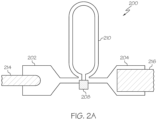
- an improved strap/bridge circuit 200 is disclosed.
- the overlap between each of the coil ends of the antenna coil and the associated coupling pads can be configured to be different.
- the inner coil end 214 of the coil antenna can be configured to be smaller than the outer coil end 216 of the coil antenna.
- the first coupling pad 202 and second coupling pad 204 can be coupled to the inner coil end 214 and outer coil end 216 respectively via an adhesive that acts as a dielectric between the coil ends and coupling pads.
- FIG. 2A shows changes in dimensions only for the coil ends, in other embodiments the sizes of one or more of the coil ends and/or one of more of the coupling pads can be configured to be different as would be understood in the art.
- the circuit resonates at a resonant frequency that is determined by the inductance of the antenna coil and tuning coil, and the total capacitance determined by the configuration of the coil ends and coupling pads.
- a common current flows through the capacitors C 1 and C 2 .
- the voltage across each of the capacitors C 1 and C 2 is inversely proportional to the capacitance of each. Therefore, by minimizing C 1 and maximizing C 2 it is possible to develop a higher voltage across C 1 than C 2 . In this way, the highest possible voltage for a given field strength is developed across C 1 .
- the dielectric (adhesive) used to couple the coil end to the coupling pad can be formulated to undergo a dielectric breakdown at a threshold breakdown voltage that is lower than the voltage presented at C 1 but higher than the voltage presented at C 2 .
- the breakdown voltage can be selected by changing the dielectric constant, the conductivity, thickness, or other suitable property of the dielectic (adhesive) so as to make any resonance of the circuit undetectable by an EAS gate reader system.
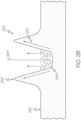
- one or more points of separation can be reduced between capacitor places. This can be achieved by embossing or otherwise mechanically modifying the metal layers of capacitor plates. Similarly, to reduce the breakdown voltage for C 1 or C 2 , one or more points of separation can be reduced between a coil end and a coupling pad. Referring now to FIG. 2B , a structure 220 on the metal surface 222 of a coil end (and/or a coupling pad) can be made using a laser system.
- a laser beam 224 causes metal to evaporate at the impact point 226 of the laser beam 224, that also melts adjacent metal 228 which is forced away and up by the pressure of the evaporating metal at the impact point 226.
- multiple points on one or more metal surfaces 222 can be made to decrease the breakdown voltage.
- the UHF tuning loop 110, 210 can be configured to change properties when a high current flows through the UHF tuning loop 110, 210.
- the UHF tuning loop 110, 210 can include a fuse type structure that causes the UHF tuning loop 110, 210 to become an open circuit above a threshold AC current.
- the UHF tuning loop 110, 210 can become an open circuit when the EAS function of the circuit is de-activated.
- the tuning of the entire circuit can be changed, leading to a changed read range.
- the read range can be greatly reduced or substantially eliminated.
- Example fuse type structures can include, but are not limited to, polymers with conductive particles and/or structures that normally have a low resistance but which under localized heating caused by a high AC current are caused to expand non-reversibly and have a high resistance.
- a dual mode strap 300 is illustrated that is configured for both a UHF response and a resonance suitable for triggering an EAS gate.
- the dual mode strap 300 includes asymmetric coupling pads and includes a relatively large coupling pad 302 and a relatively small coupling pad 304 that are coupled to a UHF RFID chip 308.
- the large coupling pad 302 is configured to be large enough to support a first coupling area 310 and a second coupling area 312.
- the large coupling pad 302 is configured to function as a bridge across the coil ends of an antenna coil with a defined capacitance set by the adhesive properties and the overlaps areas as describe above.
- the small coupling pad 302 is configured to support a third coupling area 314 for coupling to an additional UHF antenna element 318.
- the dual mode strap 300 can therefore support both resonant absorption for EAS functionality and UHF RFID functionality as the UHF RFID chip 308 is coupled to the coil antenna at one end and a UHF RFID antenna at the other end.
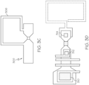
- the first coupling area 310, the second coupling area 312, and/or the third coupling area 314 can be a different size than the overlap area; for example the coupling area can be smaller than the overlap area as illustrated in FIG. 3B .
- the dual mode strap 300 of FIGS. 3A and 3B can include a UHF tuning loop 306. Because both coil ends of the coil antenna of FIG. 3B are coupled to the large coupling pad 302 (and not the small coupling pad 304), the UHF tuning loop 306 can be positioned as shown in FIG. 3C so as to be offset from the coil antenna to avoid interference. As described above, the UHF tuning loop 306 can include a fuse type structure that causes the UHF tuning loop 306 to open circuit above a threshold AC current, for example when the EAS function of the circuit is de-activated.
- the first coupling point 310 and second coupling point 312 can be configured to be asymmetric in size so as to concentrate voltage at one of the coupling points (e.g., second coupling point 312, as shown in FIG. 3(d) ) for de-activating the circuit by exposing the circuit to a high strength field at the resonant frequency of the circuit.
- the coupling points e.g., second coupling point 312, as shown in FIG. 3(d)
- the modified coil antenna structure 400 is configured to have a large coil with a narrow gap width 402 between turns. This causes the coil antenna to act a sloop type antenna such that at UHF frequencies, the energy couples across the narrow gap width 402 to form a short at UHF frequencies, but which allows energy at HF frequencies to flow around the coil antenna turns normally.
- the coil antenna can include a wider gap width 404 for a portion of the coil antenna for UHF frequencies.
- a strap 406, tuning loop 408, and RFID chip 410 are included as described previously for other embodiments.
- the coupling between the turns can be enhanced by decreasing the gap width by, for example, laser cutting a narrow gap 420 as illustrated in FIG. 4A , and/or by increasing the relative edge-to-edge area between turns by cutting a curvilinear gap 422 (or cutting any suitable pattern) as illustrated in FIG. 4B .
- a first embodiment of a foldover circuit 500 is presented.
- the foldover circuit 500 can be configured such that when the foldover circuit 500 is folded at a fold line 502, coupling pad 508 of the strap 510 functions as a bridge for coil antenna 512.
- Coupling pad 508 can be conductively coupled to a first coil end 504 of coil antenna 512.
- coupling pad 508 can be capacitively coupled to second coil end 506 of coil antenna 512, for example using a dielectric adhesive as described above.
- an additional UHF antenna element 518 can be capacitively coupled to the strap 510 when the foldover circuit 500 is folded.
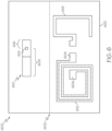
- Foldover circuit 600 can be configured such that when the foldover circuit 600 is folded at fold line 602, a bridge portion 608 (first coupling pad) of the strap 610 contacts a first coil end 606 and a second coil end 608 of coil antenna 612.
- the bridge portion 608 and coil ends 606, 608 are capacitively coupled using a dielectric adhesive as described above.
- an additional UHF antenna element 618 can be capacitively coupled to a UHF portion 616 (second coupling pad) of the strap 610 when the foldover circuit 600 is folded.
- the strap 610 and RFID chip 614 can be configured on one side of a substrate 620, while the coil antenna 612 and UHF antenna element 618 can be configured on a second side of the substrate 620.
- the substrate 620 can comprise any suitable material including, but not limited to, a paper, a card, a plastic such as PET, or a fabric such as nylon or polypropylene.
- the substrate 620 can be folded at fold line 602 and the two sides laminated together.
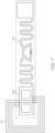
- a portion of a UHF antenna 718 functions as a bridge.
- a structure at the end of a UHF antenna 718 commonly described as a top load 720, and comprising a relatively large area of conductor functions as the resonating capacitor in the circuit with the coil antenna 712.
- the UHF antenna 718 can be applied to the coil antenna 712 or the coil antenna 712 can be applied to the top load 720 portion of the UHF antenna 718.
- the RFID chip can be directly attached, commonly described as a flip chip, or can be built with a strap as described above, and can be attached before or after the coil antenna 712. Additional details about the manufacture and use of RFID straps are described in U.S. Patent No. 7,158,037 and U.S. Patent No. 7,292,148 , each incorporated herein by reference in their respective entireties.
Landscapes
- Engineering & Computer Science (AREA)
- Physics & Mathematics (AREA)
- General Physics & Mathematics (AREA)
- Microelectronics & Electronic Packaging (AREA)
- Theoretical Computer Science (AREA)
- Computer Hardware Design (AREA)
- Computer Networks & Wireless Communication (AREA)
- Automation & Control Theory (AREA)
- Computer Security & Cryptography (AREA)
- Electromagnetism (AREA)
- Details Of Aerials (AREA)
- Support Of Aerials (AREA)
- Variable-Direction Aerials And Aerial Arrays (AREA)
Applications Claiming Priority (4)
| Application Number | Priority Date | Filing Date | Title |
|---|---|---|---|
| US201662440131P | 2016-12-29 | 2016-12-29 | |
| EP17835981.6A EP3563297B1 (fr) | 2016-12-29 | 2017-12-29 | Sangle à double fonction pour éléments résonants et antennes à ultra haute fréquence |
| EP23182083.8A EP4235967B1 (fr) | 2016-12-29 | 2017-12-29 | Sangle à double fonction pour éléments résonants et antennes à ultra haute fréquence |
| PCT/US2017/068961 WO2018126137A2 (fr) | 2016-12-29 | 2017-12-29 | Sangle à double fonction pour éléments résonants et antennes à ultra haute fréquence |
Related Parent Applications (2)
| Application Number | Title | Priority Date | Filing Date |
|---|---|---|---|
| EP17835981.6A Division EP3563297B1 (fr) | 2016-12-29 | 2017-12-29 | Sangle à double fonction pour éléments résonants et antennes à ultra haute fréquence |
| EP23182083.8A Division EP4235967B1 (fr) | 2016-12-29 | 2017-12-29 | Sangle à double fonction pour éléments résonants et antennes à ultra haute fréquence |
Publications (2)
| Publication Number | Publication Date |
|---|---|
| EP4539254A2 true EP4539254A2 (fr) | 2025-04-16 |
| EP4539254A3 EP4539254A3 (fr) | 2025-07-16 |
Family
ID=61074514
Family Applications (3)
| Application Number | Title | Priority Date | Filing Date |
|---|---|---|---|
| EP23182083.8A Active EP4235967B1 (fr) | 2016-12-29 | 2017-12-29 | Sangle à double fonction pour éléments résonants et antennes à ultra haute fréquence |
| EP25153116.6A Pending EP4539254A3 (fr) | 2016-12-29 | 2017-12-29 | Sangle à double fonction pour éléments résonants et antennes à ultra haute fréquence |
| EP17835981.6A Active EP3563297B1 (fr) | 2016-12-29 | 2017-12-29 | Sangle à double fonction pour éléments résonants et antennes à ultra haute fréquence |
Family Applications Before (1)
| Application Number | Title | Priority Date | Filing Date |
|---|---|---|---|
| EP23182083.8A Active EP4235967B1 (fr) | 2016-12-29 | 2017-12-29 | Sangle à double fonction pour éléments résonants et antennes à ultra haute fréquence |
Family Applications After (1)
| Application Number | Title | Priority Date | Filing Date |
|---|---|---|---|
| EP17835981.6A Active EP3563297B1 (fr) | 2016-12-29 | 2017-12-29 | Sangle à double fonction pour éléments résonants et antennes à ultra haute fréquence |
Country Status (6)
| Country | Link |
|---|---|
| US (3) | US10679478B2 (fr) |
| EP (3) | EP4235967B1 (fr) |
| JP (1) | JP6987867B2 (fr) |
| CN (2) | CN110100254B (fr) |
| BR (1) | BR112019012977A8 (fr) |
| WO (1) | WO2018126137A2 (fr) |
Families Citing this family (13)
| Publication number | Priority date | Publication date | Assignee | Title |
|---|---|---|---|---|
| CN102668241B (zh) * | 2010-03-24 | 2015-01-28 | 株式会社村田制作所 | Rfid系统 |
| USD840983S1 (en) * | 2017-10-20 | 2019-02-19 | Avery Dennison Retail Information Services, Llc | RFID inlay |
| EP3973454A1 (fr) | 2019-05-23 | 2022-03-30 | Sml Intelligent Inventory Solutions Llc | Étiquettes mixtes rfid/eas et procédés de fabrication |
| US12265870B2 (en) | 2019-05-23 | 2025-04-01 | Sml Intelligent Inventory Solutions Llc | Combination RFID/EAS tags and methods of manufacture |
| US20220222501A1 (en) * | 2019-05-28 | 2022-07-14 | Avery Dennison Retail Information Services Llc | Radio Frequency Identification (RFID) Tags for Metallic and Three-Dimensional (3D) Objects and Methods of Making and Using Thereof |
| CN114586041A (zh) | 2019-08-28 | 2022-06-03 | 艾利丹尼森零售信息服务有限公司 | 旋转不敏感型射频识别器件和形成该器件的方法 |
| CN115136142B (zh) * | 2019-12-28 | 2025-09-02 | 艾利丹尼森零售信息服务有限公司 | 双模射频识别器件 |
| CN115087985B (zh) | 2019-12-28 | 2025-07-18 | 艾利丹尼森零售信息服务有限公司 | 与电抗型连接带联用的调谐组件方法和系统 |
| EP4418459A3 (fr) | 2019-12-28 | 2024-11-13 | Avery Dennison Retail Information Services LLC | Etiquettes d'identification par radiofrequence pour objets tridimensionnels |
| CN115335880B (zh) * | 2020-02-06 | 2024-12-24 | 艾利丹尼森零售信息服务有限公司 | 用于增加射频识别电子物品监视系统的可靠性和有效性的射频识别装置的控制 |
| FR3111022B1 (fr) | 2020-05-28 | 2023-01-20 | Centre Technique Du Papier | Dispositif de radio-identification comprenant un élément de jonction |
| USD1005271S1 (en) | 2021-10-15 | 2023-11-21 | Avery Dennison Retail Information Services Llc | Antenna |
| WO2025006654A1 (fr) * | 2023-06-29 | 2025-01-02 | Checkpoint Systems, Inc. | Circuit eas et étiquette |
Citations (2)
| Publication number | Priority date | Publication date | Assignee | Title |
|---|---|---|---|---|
| US7158037B2 (en) | 2004-03-22 | 2007-01-02 | Avery Dennison Corporation | Low cost method of producing radio frequency identification tags with straps without antenna patterning |
| US7292148B2 (en) | 2004-06-18 | 2007-11-06 | Avery Dennison Corporation | Method of variable position strap mounting for RFID transponder |
Family Cites Families (37)
| Publication number | Priority date | Publication date | Assignee | Title |
|---|---|---|---|---|
| US5103210A (en) * | 1990-06-27 | 1992-04-07 | Checkpoint Systems, Inc. | Activatable/deactivatable security tag for use with an electronic security system |
| JP4195164B2 (ja) * | 2000-01-31 | 2008-12-10 | トッパン・フォームズ株式会社 | Icチップの実装方法 |
| US6407669B1 (en) * | 2001-02-02 | 2002-06-18 | 3M Innovative Properties Company | RFID tag device and method of manufacturing |
| US6667092B1 (en) * | 2002-09-26 | 2003-12-23 | International Paper Company | RFID enabled corrugated structures |
| US7224280B2 (en) * | 2002-12-31 | 2007-05-29 | Avery Dennison Corporation | RFID device and method of forming |
| JP4829242B2 (ja) * | 2004-10-22 | 2011-12-07 | 株式会社サトー | ラベルおよびラベルを物体に貼付するための方法 |
| US7452748B1 (en) * | 2004-11-08 | 2008-11-18 | Alien Technology Corporation | Strap assembly comprising functional block deposited therein and method of making same |
| US7804411B2 (en) * | 2004-11-15 | 2010-09-28 | Sensormatic Electronics, LLC | Combination EAS and RFID label or tag using a hybrid RFID antenna |
| FR2901041B1 (fr) * | 2006-05-12 | 2008-10-10 | Eric Heurtier | Etiquette integrant une antenne anti-vol rf et un transporteur rfid uhf |
| US8794531B2 (en) * | 2006-07-13 | 2014-08-05 | Confidex Oy | Radio frequency identification tag |
| US8381991B2 (en) * | 2006-12-18 | 2013-02-26 | Mikoh Company | Radio frequency identification tag with privacy and security capabilities |
| US8026818B2 (en) * | 2006-12-20 | 2011-09-27 | Checkpoint Systems, Inc. | EAS and UHF combination tag |
| US7768407B2 (en) * | 2007-06-22 | 2010-08-03 | Avery Dennison Corporation | Foldable RFID device interposer and method |
| US8633821B2 (en) * | 2007-12-03 | 2014-01-21 | Avery Dennison Corporation | Dual use RFID/EAS device |
| US10339436B2 (en) * | 2015-05-21 | 2019-07-02 | Smartrac Technology Fletcher, Inc. | Multi-frequency radio frequency identification tag |
| US10262167B2 (en) * | 2008-01-31 | 2019-04-16 | Smartrac Technology Fletcher, Inc. | Detachable radio frequency identification switch tag |
| US8056814B2 (en) * | 2008-02-27 | 2011-11-15 | Tagsys Sas | Combined EAS/RFID tag |
| EP2286391B1 (fr) | 2008-05-15 | 2019-08-14 | Thin Film Electronics ASA | Dispositifs de surveillance avec multiples condensateurs |
| WO2010059721A1 (fr) * | 2008-11-19 | 2010-05-27 | 3M Innovative Properties Company | Antenne d'étiquette rfid à composant d'accord couplé de manière capacitive ou inductive |
| EP2366271B1 (fr) * | 2008-11-25 | 2019-03-20 | Thin Film Electronics ASA | Antennes imprimées, procédés d'impression d'une antenne et dispositifs incluant l'antenne imprimée |
| US8350702B2 (en) * | 2009-07-01 | 2013-01-08 | Sensormatic Electronics, LLC | Combination EAS and RFID security tag having structure for orienting a hybrid antenna RFID element |
| US8833664B2 (en) * | 2009-12-18 | 2014-09-16 | Yu Yung Choi | Enhanced performance and security RFID device |
| US10026035B2 (en) * | 2011-03-24 | 2018-07-17 | Avery Dennison Retail Information Services, Llc | RFID tag including a coating |
| EP2525304A1 (fr) * | 2011-05-17 | 2012-11-21 | Gemalto SA | Dispositif transpondeur radiofréquence à circuit résonant passif optimisé |
| JP2012248106A (ja) * | 2011-05-30 | 2012-12-13 | Toppan Printing Co Ltd | 非接触icラベル |
| EP2754100B1 (fr) * | 2011-09-08 | 2017-08-09 | Avery Dennison Corporation | Dispositif rfid à structure allongée |
| US8763913B2 (en) * | 2011-10-25 | 2014-07-01 | International Business Machines Corporation | RFID tag integrated into an enclosure surface door |
| US9342775B2 (en) * | 2011-11-01 | 2016-05-17 | Avery Dennison Corporation | Dual mode chip having radio frequency identification and electronic article surveillance capability |
| US9058554B2 (en) * | 2011-11-25 | 2015-06-16 | Smartrac Ip B.V. | Transponder with tamper protection |
| JP2013205903A (ja) * | 2012-03-27 | 2013-10-07 | Toppan Printing Co Ltd | Icラベル |
| EP2836878B1 (fr) * | 2012-04-11 | 2019-02-27 | IMPINJ, Inc. | Circuits intégrés de rfid et étiquettes présentant des contacts d'antenne sur des surfaces multiples |
| CN103530680B (zh) * | 2013-09-16 | 2016-08-17 | 杭州电子科技大学 | 一种双频射频识别标签以及包括该标签的射频识别系统 |
| US9390603B2 (en) * | 2014-09-24 | 2016-07-12 | Checkpoint Systems, Inc. | Dual EAS-RFID security tag |
| US9953193B2 (en) * | 2014-09-30 | 2018-04-24 | Tego, Inc. | Operating systems for an RFID tag |
| US9582750B2 (en) * | 2014-12-22 | 2017-02-28 | Avery Dennison Retail Information Services, Llc | RFID devices with multi-frequency antennae |
| CN204463187U (zh) * | 2014-12-30 | 2015-07-08 | 江苏联恒物宇科技有限公司 | 一种基于新型eas和uhf标签的双频卡 |
| US10186126B2 (en) * | 2015-09-15 | 2019-01-22 | Avery Dennison Retail Information Services, Llc | Multi-port straps incorporating sensing features |
-
2017
- 2017-12-29 CN CN201780079451.0A patent/CN110100254B/zh active Active
- 2017-12-29 EP EP23182083.8A patent/EP4235967B1/fr active Active
- 2017-12-29 JP JP2019534941A patent/JP6987867B2/ja active Active
- 2017-12-29 US US15/858,363 patent/US10679478B2/en active Active
- 2017-12-29 WO PCT/US2017/068961 patent/WO2018126137A2/fr not_active Ceased
- 2017-12-29 EP EP25153116.6A patent/EP4539254A3/fr active Pending
- 2017-12-29 EP EP17835981.6A patent/EP3563297B1/fr active Active
- 2017-12-29 CN CN202311313012.5A patent/CN117391116A/zh active Pending
- 2017-12-29 BR BR112019012977A patent/BR112019012977A8/pt not_active Application Discontinuation
-
2020
- 2020-06-08 US US16/895,906 patent/US11488459B2/en active Active
-
2022
- 2022-09-22 US US17/934,354 patent/US11704985B2/en active Active
Patent Citations (2)
| Publication number | Priority date | Publication date | Assignee | Title |
|---|---|---|---|---|
| US7158037B2 (en) | 2004-03-22 | 2007-01-02 | Avery Dennison Corporation | Low cost method of producing radio frequency identification tags with straps without antenna patterning |
| US7292148B2 (en) | 2004-06-18 | 2007-11-06 | Avery Dennison Corporation | Method of variable position strap mounting for RFID transponder |
Also Published As
| Publication number | Publication date |
|---|---|
| EP3563297B1 (fr) | 2023-07-05 |
| BR112019012977A2 (pt) | 2019-12-31 |
| US20200302764A1 (en) | 2020-09-24 |
| WO2018126137A2 (fr) | 2018-07-05 |
| US20230012595A1 (en) | 2023-01-19 |
| EP3563297A2 (fr) | 2019-11-06 |
| US10679478B2 (en) | 2020-06-09 |
| US11488459B2 (en) | 2022-11-01 |
| JP6987867B2 (ja) | 2022-01-05 |
| EP4235967B1 (fr) | 2025-01-29 |
| EP4235967A3 (fr) | 2023-11-01 |
| BR112019012977A8 (pt) | 2023-02-28 |
| CN117391116A (zh) | 2024-01-12 |
| CN110100254A (zh) | 2019-08-06 |
| US11704985B2 (en) | 2023-07-18 |
| EP4235967A2 (fr) | 2023-08-30 |
| EP4539254A3 (fr) | 2025-07-16 |
| CN110100254B (zh) | 2023-10-27 |
| JP2020503771A (ja) | 2020-01-30 |
| WO2018126137A3 (fr) | 2018-08-16 |
| US20180211499A1 (en) | 2018-07-26 |
Similar Documents
| Publication | Publication Date | Title |
|---|---|---|
| US11704985B2 (en) | Dual function strap for resonating elements and ultra high frequency antennas | |
| US8289165B2 (en) | RFID device with conductive loop shield | |
| JP4393228B2 (ja) | 小型アンテナ及びそれを備えた無線タグ | |
| US20210367325A1 (en) | Wireless communication device | |
| JP6345588B2 (ja) | 近距離場用途用小型広帯域ループ・アンテナ | |
| JP5051213B2 (ja) | 無線通信装置 | |
| EP3782077B1 (fr) | Procédé d'utilisation de straps rfid blindés avec des modèles d'étiquettes rfid | |
| US20210365758A1 (en) | Planar conductive device that forms a coil for an rfid tag when folded | |
| JP5051211B2 (ja) | 無線通信装置 | |
| CN211238502U (zh) | 无线通信设备 | |
| EP3611670B1 (fr) | Étiquette rfid et matériau attaché à un rfid | |
| US20250096474A1 (en) | Dual rfid antenna | |
| JP2011128956A (ja) | 無線通信装置 | |
| US11101567B2 (en) | Miniaturized planar inverted folded antenna (PIFA) for mountable UHF tags design | |
| US9460379B2 (en) | RF tag with resonant circuit structure | |
| JP5312587B2 (ja) | 無線通信装置 |
Legal Events
| Date | Code | Title | Description |
|---|---|---|---|
| PUAI | Public reference made under article 153(3) epc to a published international application that has entered the european phase |
Free format text: ORIGINAL CODE: 0009012 |
|
| STAA | Information on the status of an ep patent application or granted ep patent |
Free format text: STATUS: THE APPLICATION HAS BEEN PUBLISHED |
|
| AC | Divisional application: reference to earlier application |
Ref document number: 3563297 Country of ref document: EP Kind code of ref document: P Ref document number: 4235967 Country of ref document: EP Kind code of ref document: P |
|
| AK | Designated contracting states |
Kind code of ref document: A2 Designated state(s): AL AT BE BG CH CY CZ DE DK EE ES FI FR GB GR HR HU IE IS IT LI LT LU LV MC MK MT NL NO PL PT RO RS SE SI SK SM TR |
|
| REG | Reference to a national code |
Ref country code: DE Ref legal event code: R079 Free format text: PREVIOUS MAIN CLASS: H01Q0007000000 Ipc: G06K0019070000 |
|
| PUAL | Search report despatched |
Free format text: ORIGINAL CODE: 0009013 |
|
| AK | Designated contracting states |
Kind code of ref document: A3 Designated state(s): AL AT BE BG CH CY CZ DE DK EE ES FI FR GB GR HR HU IE IS IT LI LT LU LV MC MK MT NL NO PL PT RO RS SE SI SK SM TR |
|
| RIC1 | Information provided on ipc code assigned before grant |
Ipc: G06K 19/07 20060101AFI20250610BHEP Ipc: G06K 19/077 20060101ALI20250610BHEP Ipc: H01Q 1/22 20060101ALI20250610BHEP Ipc: H01Q 7/00 20060101ALI20250610BHEP |
|
| STAA | Information on the status of an ep patent application or granted ep patent |
Free format text: STATUS: REQUEST FOR EXAMINATION WAS MADE |
|
| 17P | Request for examination filed |
Effective date: 20251211 |
|
| STAA | Information on the status of an ep patent application or granted ep patent |
Free format text: STATUS: EXAMINATION IS IN PROGRESS |
|
| 17Q | First examination report despatched |
Effective date: 20260326 |