EP4557537A1 - Integrierte hochleistungslaseremissionsvorrichtung - Google Patents
Integrierte hochleistungslaseremissionsvorrichtung Download PDFInfo
- Publication number
- EP4557537A1 EP4557537A1 EP24213431.0A EP24213431A EP4557537A1 EP 4557537 A1 EP4557537 A1 EP 4557537A1 EP 24213431 A EP24213431 A EP 24213431A EP 4557537 A1 EP4557537 A1 EP 4557537A1
- Authority
- EP
- European Patent Office
- Prior art keywords
- waveguide
- reflector
- main
- spectral band
- reflection
- Prior art date
- Legal status (The legal status is an assumption and is not a legal conclusion. Google has not performed a legal analysis and makes no representation as to the accuracy of the status listed.)
- Pending
Links
Images


Classifications
-
- H—ELECTRICITY
- H01—ELECTRIC ELEMENTS
- H01S—DEVICES USING THE PROCESS OF LIGHT AMPLIFICATION BY STIMULATED EMISSION OF RADIATION [LASER] TO AMPLIFY OR GENERATE LIGHT; DEVICES USING STIMULATED EMISSION OF ELECTROMAGNETIC RADIATION IN WAVE RANGES OTHER THAN OPTICAL
- H01S5/00—Semiconductor lasers
- H01S5/02—Structural details or components not essential to laser action
- H01S5/026—Monolithically integrated components, e.g. waveguides, monitoring photo-detectors, drivers
-
- H—ELECTRICITY
- H01—ELECTRIC ELEMENTS
- H01S—DEVICES USING THE PROCESS OF LIGHT AMPLIFICATION BY STIMULATED EMISSION OF RADIATION [LASER] TO AMPLIFY OR GENERATE LIGHT; DEVICES USING STIMULATED EMISSION OF ELECTROMAGNETIC RADIATION IN WAVE RANGES OTHER THAN OPTICAL
- H01S5/00—Semiconductor lasers
- H01S5/10—Construction or shape of the optical resonator, e.g. extended or external cavity, coupled cavities, bent-guide, varying width, thickness or composition of the active region
- H01S5/14—External cavity lasers
- H01S5/141—External cavity lasers using a wavelength selective device, e.g. a grating or etalon
-
- H—ELECTRICITY
- H01—ELECTRIC ELEMENTS
- H01S—DEVICES USING THE PROCESS OF LIGHT AMPLIFICATION BY STIMULATED EMISSION OF RADIATION [LASER] TO AMPLIFY OR GENERATE LIGHT; DEVICES USING STIMULATED EMISSION OF ELECTROMAGNETIC RADIATION IN WAVE RANGES OTHER THAN OPTICAL
- H01S5/00—Semiconductor lasers
- H01S5/02—Structural details or components not essential to laser action
- H01S5/0206—Substrates, e.g. growth, shape, material, removal or bonding
- H01S5/021—Silicon based substrates
-
- H—ELECTRICITY
- H01—ELECTRIC ELEMENTS
- H01S—DEVICES USING THE PROCESS OF LIGHT AMPLIFICATION BY STIMULATED EMISSION OF RADIATION [LASER] TO AMPLIFY OR GENERATE LIGHT; DEVICES USING STIMULATED EMISSION OF ELECTROMAGNETIC RADIATION IN WAVE RANGES OTHER THAN OPTICAL
- H01S5/00—Semiconductor lasers
- H01S5/06—Arrangements for controlling the laser output parameters, e.g. by operating on the active medium
- H01S5/062—Arrangements for controlling the laser output parameters, e.g. by operating on the active medium by varying the potential of the electrodes
- H01S5/0625—Arrangements for controlling the laser output parameters, e.g. by operating on the active medium by varying the potential of the electrodes in multi-section lasers
- H01S5/06255—Controlling the frequency of the radiation
- H01S5/06256—Controlling the frequency of the radiation with DBR-structure
-
- H—ELECTRICITY
- H01—ELECTRIC ELEMENTS
- H01S—DEVICES USING THE PROCESS OF LIGHT AMPLIFICATION BY STIMULATED EMISSION OF RADIATION [LASER] TO AMPLIFY OR GENERATE LIGHT; DEVICES USING STIMULATED EMISSION OF ELECTROMAGNETIC RADIATION IN WAVE RANGES OTHER THAN OPTICAL
- H01S5/00—Semiconductor lasers
- H01S5/06—Arrangements for controlling the laser output parameters, e.g. by operating on the active medium
- H01S5/065—Mode locking; Mode suppression; Mode selection ; Self pulsating
- H01S5/0651—Mode control
- H01S5/0653—Mode suppression, e.g. specific multimode
- H01S5/0654—Single longitudinal mode emission
-
- H—ELECTRICITY
- H01—ELECTRIC ELEMENTS
- H01S—DEVICES USING THE PROCESS OF LIGHT AMPLIFICATION BY STIMULATED EMISSION OF RADIATION [LASER] TO AMPLIFY OR GENERATE LIGHT; DEVICES USING STIMULATED EMISSION OF ELECTROMAGNETIC RADIATION IN WAVE RANGES OTHER THAN OPTICAL
- H01S5/00—Semiconductor lasers
- H01S5/10—Construction or shape of the optical resonator, e.g. extended or external cavity, coupled cavities, bent-guide, varying width, thickness or composition of the active region
- H01S5/1003—Waveguide having a modified shape along the axis, e.g. branched, curved, tapered, voids
- H01S5/1007—Branched waveguides
-
- H—ELECTRICITY
- H01—ELECTRIC ELEMENTS
- H01S—DEVICES USING THE PROCESS OF LIGHT AMPLIFICATION BY STIMULATED EMISSION OF RADIATION [LASER] TO AMPLIFY OR GENERATE LIGHT; DEVICES USING STIMULATED EMISSION OF ELECTROMAGNETIC RADIATION IN WAVE RANGES OTHER THAN OPTICAL
- H01S5/00—Semiconductor lasers
- H01S5/10—Construction or shape of the optical resonator, e.g. extended or external cavity, coupled cavities, bent-guide, varying width, thickness or composition of the active region
- H01S5/12—Construction or shape of the optical resonator, e.g. extended or external cavity, coupled cavities, bent-guide, varying width, thickness or composition of the active region the resonator having a periodic structure, e.g. in distributed feedback [DFB] lasers
- H01S5/125—Distributed Bragg reflector [DBR] lasers
-
- H—ELECTRICITY
- H01—ELECTRIC ELEMENTS
- H01S—DEVICES USING THE PROCESS OF LIGHT AMPLIFICATION BY STIMULATED EMISSION OF RADIATION [LASER] TO AMPLIFY OR GENERATE LIGHT; DEVICES USING STIMULATED EMISSION OF ELECTROMAGNETIC RADIATION IN WAVE RANGES OTHER THAN OPTICAL
- H01S5/00—Semiconductor lasers
- H01S5/10—Construction or shape of the optical resonator, e.g. extended or external cavity, coupled cavities, bent-guide, varying width, thickness or composition of the active region
- H01S5/14—External cavity lasers
- H01S5/141—External cavity lasers using a wavelength selective device, e.g. a grating or etalon
- H01S5/142—External cavity lasers using a wavelength selective device, e.g. a grating or etalon which comprises an additional resonator
-
- H—ELECTRICITY
- H01—ELECTRIC ELEMENTS
- H01S—DEVICES USING THE PROCESS OF LIGHT AMPLIFICATION BY STIMULATED EMISSION OF RADIATION [LASER] TO AMPLIFY OR GENERATE LIGHT; DEVICES USING STIMULATED EMISSION OF ELECTROMAGNETIC RADIATION IN WAVE RANGES OTHER THAN OPTICAL
- H01S5/00—Semiconductor lasers
- H01S5/40—Arrangement of two or more semiconductor lasers, not provided for in groups H01S5/02 - H01S5/30
- H01S5/4012—Beam combining, e.g. by the use of fibres, gratings, polarisers, prisms
-
- H—ELECTRICITY
- H01—ELECTRIC ELEMENTS
- H01S—DEVICES USING THE PROCESS OF LIGHT AMPLIFICATION BY STIMULATED EMISSION OF RADIATION [LASER] TO AMPLIFY OR GENERATE LIGHT; DEVICES USING STIMULATED EMISSION OF ELECTROMAGNETIC RADIATION IN WAVE RANGES OTHER THAN OPTICAL
- H01S5/00—Semiconductor lasers
- H01S5/40—Arrangement of two or more semiconductor lasers, not provided for in groups H01S5/02 - H01S5/30
- H01S5/4025—Array arrangements, e.g. constituted by discrete laser diodes or laser bar
- H01S5/4031—Edge-emitting structures
- H01S5/4062—Edge-emitting structures with an external cavity or using internal filters, e.g. Talbot filters
-
- H—ELECTRICITY
- H01—ELECTRIC ELEMENTS
- H01S—DEVICES USING THE PROCESS OF LIGHT AMPLIFICATION BY STIMULATED EMISSION OF RADIATION [LASER] TO AMPLIFY OR GENERATE LIGHT; DEVICES USING STIMULATED EMISSION OF ELECTROMAGNETIC RADIATION IN WAVE RANGES OTHER THAN OPTICAL
- H01S5/00—Semiconductor lasers
- H01S5/40—Arrangement of two or more semiconductor lasers, not provided for in groups H01S5/02 - H01S5/30
- H01S5/4025—Array arrangements, e.g. constituted by discrete laser diodes or laser bar
- H01S5/4031—Edge-emitting structures
- H01S5/4068—Edge-emitting structures with lateral coupling by axially offset or by merging waveguides, e.g. Y-couplers
Definitions
- the technical field of the invention is integrated optics and more precisely the design of a high-power laser emission circuit intended to be used, in a non-limiting manner, in LIDAR or telecoms type applications, or other photonic applications.
- the use of wavelength-modulated laser sources is common.
- FMCW frequency-modulated continuous wave
- a portion of an emitted laser beam is sampled and directed toward a photodetector.
- the laser beam reflected by a target is also directed toward the photodetector. Since the sampled beam and the reflected beam are coherent, their interference can be detected by the photodetector and results in a frequency difference directly proportional to the distance from the target.
- the operation of such devices is, for example, described in C. Poulton's publication "Coherent solid-state LIDAR with silicon photonic optical phased arrays.”
- wavelength-modulated lasers can also concern the field of optical telecommunications.
- the document US2020/161831 describes a laser source intended to emit a wavelength while minimizing drift under the effect of a temperature variation.
- the invention described below makes it possible to obtain a laser source integrated into a monolithic substrate.
- a high-power laser source or several laser sources are obtained.
- the laser source is continuously wavelength modulated, which allows it to be used in Lidars.
- the main reflector or each secondary reflector is adjustable, so as to modulate the reflection spectral band.
- the reflection spectral band of the main reflector is adjustable, the main reflector being a Bragg mirror, coupled to a modulator configured to modulate a refractive index in said Bragg mirror.
- Each secondary reflector can reflect light in a fixed secondary reflection spectral band wider than, and containing, the reflection spectral band of the main reflector.
- each secondary reflector is adjustable, each secondary reflector being a Bragg mirror, coupled to a modulator configured to modulate a refractive index in said Bragg mirror.
- the main reflector can reflect light in a fixed reflection spectral band wider than, and containing, the reflection spectral band of each secondary reflector.
- At least one secondary waveguide comprises a secondary phase modulator, configured to modulate a refractive index along a portion of said secondary waveguide, the secondary phase modulator being disposed between the coupling end of said secondary waveguide and the secondary reflector of said secondary waveguide, so as to modulate an optical path in said secondary waveguide.
- a secondary phase modulator configured to modulate a refractive index along a portion of said secondary waveguide, the secondary phase modulator being disposed between the coupling end of said secondary waveguide and the secondary reflector of said secondary waveguide, so as to modulate an optical path in said secondary waveguide.
- each secondary waveguide comprises a secondary phase modulator, configured to modulate a refractive index along a portion of said secondary waveguide, the secondary phase modulator being disposed between the coupling end of said secondary waveguide and the secondary reflector of said secondary waveguide, so as to modulate an optical path in each secondary waveguide.
- the main waveguide may comprise a main phase modulator, configured to modulate a refractive index along a portion of the main waveguide, the main phase modulator being disposed between each secondary waveguide and the main reflector, so as to modulate the resonant wavelength of each Fabry-Pérot cavity of the device.
- the main waveguide may be formed by a first material, and surrounded by a first auxiliary material, the refractive index of which is lower than the refractive index of the first material.
- Each secondary waveguide may be formed by a second material, and surrounded by a second auxiliary material, the refractive index of which is lower than the refractive index of the second material.
- the main waveguide and at least one secondary waveguide, or each secondary waveguide are formed in the same substrate, each amplifying medium being transferred onto said substrate.
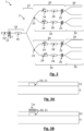
- FIG. 2 schematizes a first embodiment of a laser emission device 1 according to the invention.
- the device 1 is formed in a monolithic substrate 2.
- the Figure 2 represents a cross-sectional view of the device, in the plane of the substrate.
- Substrate 2 is for example of the SOI (Silicon on Insulator) type. SOI is a well-known substrate in microelectronics, but it is also widely used in the manufacture of integrated optical circuits.
- SOI Silicon on Insulator
- substrates can be used, for example SiNOI (acronym for Silicon Nitride on Insulator) or LNOI (acronym for Lithium Niobate on Insulator).
- SiNOI acronym for Silicon Nitride on Insulator
- LNOI acronym for Lithium Niobate on Insulator
- the device comprises a main waveguide 10, arranged in the substrate, and extending from a main reflector 15, configured to reflect a wavelength of interest.
- the main reflector 15 is a Bragg mirror, called a main Bragg mirror.
- Other types of reflectors, for example Sagnac loops, are conceivable.
- the main waveguide 10 is formed of a first material 11, in this case Si, around from which extends a first auxiliary material 12, in this case SiO 2 . Other variants are described below.
- the main waveguide 10 is formed by conventional photolithography/etching techniques. It is typically made by etching the surface silicon layer of an SOI wafer (plate), the latter being in contact with an oxide layer 3. The Si waveguide resulting from the etching is then covered with an upper layer of a lower index material 12, for example SiO 2 . The upper layer can be thinned and planarized. The thickness of the upper layer can be reduced to 100 nm. The channel is arranged on the SiO 2 layer 3. An example of channel geometry is described below, in connection with the Figures 3A and 3B The height of the waveguide 10 is typically between 220 and 500nm, and its width can vary between 100nm and 5 ⁇ m.
- the main Bragg mirror 15 is formed from a periodic alternation of two materials having different refractive indices respectively.
- the periodic variation of the index generates a set of reflections which add up when they are in phase.
- the main Bragg mirror 15 is formed by carrying out a partial etching of the silicon then depositing SiO 2 .
- the periodicity of the etched zones determines a spectral band of reflection, at which the Bragg mirror reflects the light, the period being of the order of a few hundred nanometers.
- the number of periods is typically several tens to several hundreds or even thousands.
- the device 1 comprises several secondary waveguides 20, the structure of which is preferably, but not necessarily, identical to that of the main waveguide 10: same material, same dimensions.
- each secondary waveguide 20 is formed from a second material 21, in this case Si, around which extends a second auxiliary material 22, in this case SiO 2 .
- the device 1 comprises four secondary waveguides 20.
- the number of secondary waveguides can be between 2 and 10, or even several dozen.
- each Bragg mirror can range from a few hundred microns to several millimeters.
- the reflection spectral band of the main Bragg mirror extends into the reflection spectral band of each secondary Bragg mirror. This gives reflections of at least one wavelength of interest ⁇ i , which corresponds to the intersection of the reflection spectral band of the main Bragg mirror and each secondary Bragg mirror.
- transmission waveguides 13 extend, the function of which is to provide optical coupling between the main waveguide 15 and each secondary waveguide 25.
- a coupler is used at each coupling end 23 to connect/combine the beams from the different secondary guides 20 to the main waveguide 10.
- the coupler may be, for example, a directional coupler or a multimode interferometer (MMI - MultiMode inteferometer).
- Each secondary waveguide 20 forms, with the main waveguide 10, a Fabry-Pérot cavity, allowing successive reflections of the light in the wavelength of interest ⁇ i .
- the wavelength of interest ⁇ i must also correspond to a resonance wavelength ⁇ r of each Fabry-Pérot cavity, as described below.
- the wavelength of interest ⁇ i is defined by the Bragg mirror having the narrowest reflection spectral band. This is the main Bragg mirror 15. It can be seen that the device allows the formation of as many Fabry-Pérot cavities as there are secondary waveguides 20.
- Each Fabry-Pérot cavity is formed by the main waveguide 10 and a secondary waveguide 20.
- each secondary waveguide is optically coupled to an amplification medium 24.
- the amplification medium 24, or active medium is a medium that emits laser light under the effect of pumping. It may, for example, be layers of III-V materials formed opposite the secondary waveguide 20.
- the light generated by the amplification medium 24 is injected into the secondary waveguide 20 to which it is optically coupled.
- the amplification medium 24 may be separated from the secondary waveguide 20 by a low-index bonding layer. It is known that assemblies of III-V materials of the AIGaAs/GaAs type allow emission in the 600-800 nm range, that assemblies of III-V InGaAsP/InP materials allow emission in the 1300/1500 nm range.
- the amplification layer 24 is produced by transferring, onto the substrate, a III-V laser epitaxy, allowing the formation of a few microns of active layers. This stack is then etched to form a waveguide above the photonic guide 20, itself being also optimized to facilitate light transfer to/from the III-V guide.
- the transfer of III-V material layers onto a Si waveguide formed on an SOI-type substrate is for example described in Roelkens G. “III-V/silicon photonics for on-chip and inter-chip optical interconnect”, Laser Photonics Rev. 4 No. 6, 751-779 (2010 ).
- FIG. 3A and 3B schematize cross-sectional views of the substrate 2 respectively at the level of the main waveguide 10 and at the level of the secondary waveguide 20.
- the Figure 3B schematizes a sectional view of an amplification medium 24.
- the amplification medium is configured to be coupled to a pumping system 26.
- the latter is actuated to obtain a population inversion of the charge carriers in the active material.
- This may be optical pumping, in which case the inversion results from absorption of a pump laser beam.
- it may be electrical pumping, allowing an injection of charge carriers via a current into a pin- diode whose i (intrinsic) zone is formed by the active material. Electrical pumping is simpler to implement.
- the amplifying medium 24 is arranged between the coupling end 23 and the secondary Bragg mirror 25. This allows an emission of laser light, at the wavelength of interest, which is then amplified by the Fabry Pérot cavity, because each amplifying medium 24 is arranged between two Bragg mirrors: the main Bragg mirror 15 and a secondary Bragg mirror 25.
- the emission device 1 allows an emission of a high-power, spatially distributed laser light, the emission resulting from the transmission of each secondary Bragg mirror 25.
- emission waveguides 29 allow the emission of light from the device.
- the reflection by the secondary Bragg mirrors 25 is partial.
- the part of the unreflected light is transmitted.
- Each secondary Bragg mirror 25 is arranged between a secondary waveguide 20 and at least one emission waveguide 29.
- the light waves respectively emitted by each secondary waveguide 20 are coherent, at the wavelength of interest.
- a control unit 30 makes it possible to control the modulator 17, so as to control the reflection spectral band of the main mirror 15.
- the device comprises, in each Fabry-Pérot cavity, at least one modulator, called a phase modulator, so as to modulate the resonance wavelength ⁇ r so that the latter corresponds to the wavelength of interest ⁇ i reflected by the Bragg mirrors.
- At least one of the reflectors is configured to address only one resonance peak.
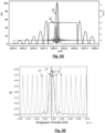
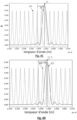
- the Figures 4A has 4D illustrate a variation in the emission wavelength of the device.
- the reflection spectral band of the main Bragg mirror 15 and the reflection spectral band of each secondary Bragg mirror 25 are represented. It is observed that the main Bragg mirror 15 reflects around 100% of the light, according to a narrow spectral band, while each secondary Bragg mirror 25 reflects around 50% of the light, according to a wide spectral band, including the narrow spectral band of the main Bragg mirror 15.
- the left y-axis is the reflectance (%), and the x-axis is the wavelength (nm).
- An intensity of the light propagating in the Fabry-Pérot cavity formed by the main Bragg mirror 15 and by the secondary Bragg mirror 25 at different wavelengths is also shown (right y-axis arbitrary unit).
- the spectral band of the main Bragg mirror 15 is represented, centered on a wavelength of interest ⁇ i close to 1550 nm.
- Resonance wavelengths ⁇ r of each Fabry-Pérot cavity are also represented on the curve referenced FP.
- the wavelength of interest ⁇ i corresponds to a resonance wavelength ⁇ r and to the emission wavelength of the device.
- the left y-axis is reflectance (%), and the x-axis is wavelength (m)
- the emission wavelength of the device corresponds to a resonance wavelength ⁇ r which is part of the reflection spectral band of the Bragg mirror, i.e. 1555 nm.
- This wavelength corresponds to the resonance wavelength of the Fabry-Pérot cavity included in the reflection spectral band.
- a discrete variation in the emission wavelength is then observed, with a jump passing from approximately 1548 nm ( Figure 4B ) at 1555 nm ( Figure 4C ). This allows the emission wavelength of the device to be modified, according to discrete values.
- the emission wavelength of the device then corresponds to a resonance wavelength present in the reflection spectral band of the main Bragg mirror.
- the left y-axis is the reflectance (%)
- the x-axis is the wavelength (m).
- the dotted lines represent the maxima of the reflection spectral bands of the main Bragg mirror before and after the shift respectively.
- the variation of the resonance wavelength ⁇ r of each Fabry Perot cavity of the device can be obtained by placing a modulator, called the main phase modulator 18, at the main waveguide 10.
- the main phase modulator 18 is configured to vary the refractive index of the main waveguide 10.
- the variation of the refractive index can be obtained by localized heating, or by charge injection.
- the main phase modulator 18 can extend over a length of between a few hundred microns and a few millimeters.
- the spectral shift can reach 0.1 nm per K.
- a spectral shift of 3 nm can be covered.
- Secondary phase modulators 28 may be arranged in each secondary waveguide. Their function is to equalize the optical paths in each secondary waveguide 20. Note that it is also possible to directly modulate the current (electrical pump signal) of each amplifying medium 24, which produces a load variation in the amplifier, and therefore a modification of the optical path. The individual adjustment makes it possible to take into account variabilities resulting from device manufacturing.
- the arrangement of secondary phase modulators 28 in each secondary waveguide allows individual adjustment of each Fabry Pérot cavity of the device, so that all cavities have, at each instant, the same resonance wavelength ⁇ r .
- the device shown on the Figure 2 may be such that the main mirror 15 is fixed, and has a wide spectral band of reflection, while each secondary mirror 25 is variable, and has a narrow spectral band of reflection.
- a configuration has the disadvantage of having to simultaneously control several secondary mirrors 25.
- the configuration shown in the Figure 2 has the advantage of only having to control one Bragg mirror, in this case the Bragg mirror 15, simultaneously with the control of the variation of the resonance wavelength of each Fabry Pérot cavity, using the main modulator 18 and/or the secondary modulators 28.
- the device comprises a photodiode 10', arranged at the output of the main mirror 10, and detecting light leaks transmitted by the latter.
- each Fabry-Pérot cavity of the device allows the emission of phase-locked lasers, which leads to a significant increase in the laser power. This increase can be detected by the photodiode 10', reflecting the proper operation of the device.
- the equalization of the optical path of each Fabry-Pérot cavity can be carried out sequentially, by adjusting each modulator and each amplifying medium one by one, to maximize the power collected at the photodiode 10'.
- the device described in connection with the Figure 2 is intended to obtain a spatially distributed coherent laser emission, at the level of each emission guide 29 connected to a secondary guide 20.
- An advantage is that the light guide transporting all the laser power is limited to the main light guide 10: the maximum power of the laser is transported over a relatively short length, typically over a few hundred microns.
- Concentrating a high power density in a single Si waveguide can lead to beam absorption by TPA (Two Photon Absorption) effect. This can lead to a limitation of the optical power emitted by the device. Distributing the beam according to different secondary waveguides 20 reduces the impact of this type of absorption.
- the main waveguide 10, which concentrates the laser power can be formed from a material less sensitive to TPA-type absorption phenomena, and more suitable for transporting high light power.
- the first material 11, forming the main waveguide possibly SiN, which does not exhibit TPA at the wavelengths of interest.
- the device described in connection with the Figure 2 allows to increase the laser power, while multiplying the emission points. It can be used in LIDAR-type systems, in order to increase their range.
- the invention can be implemented to concentrate coherent laser waves, so as to produce a high power beam.
- the components not commented on below, are identical to those described in connection with the Figure 2 , and have the same function.
- each secondary reflector 25 is totally reflective (reflection coefficient greater than 90%, or even close to 100%), while the main reflector 15 is partially reflective, the reflection coefficient being less than 80%, or even 50%.
- the emission of light is carried out by an emission waveguide 19, connected to the main waveguide 10.
- the main reflector 15 has a light extractor function.
- the main reflector 15 extends between the main waveguide 10 and the emission waveguide 19.
- the emission of light is carried out from the light transmitted by the main Bragg mirror.
- a coupler 19' makes it possible to direct a small percentage of light, for example 1%, towards the photodiode 10'. The latter is used to monitor the laser power emitted by the device. It makes it possible to verify that the phase locking of the different lasers has been obtained.
- the device can be used to emit a high-power laser beam, without necessarily varying the emission wavelength over time.
- the main modulator 18 is not necessary.
- the use of the secondary modulators 28 remains preferable, for the purpose of adjusting the optical paths in each secondary waveguide 20.
- the device can be used for photonic calculation type applications, in which mathematical operations are performed by forming destructive or constructive interference between several coherent laser beams. Constructive interference can correspond to an addition. Destructive interference corresponds to a subtraction.
Landscapes
- Physics & Mathematics (AREA)
- Condensed Matter Physics & Semiconductors (AREA)
- General Physics & Mathematics (AREA)
- Electromagnetism (AREA)
- Optics & Photonics (AREA)
- Semiconductor Lasers (AREA)
- Lasers (AREA)
- Optical Integrated Circuits (AREA)
Applications Claiming Priority (1)
| Application Number | Priority Date | Filing Date | Title |
|---|---|---|---|
| FR2312669A FR3155653A1 (fr) | 2023-11-17 | 2023-11-17 | Dispositif d’émission laser intégré de forte puissance |
Publications (1)
| Publication Number | Publication Date |
|---|---|
| EP4557537A1 true EP4557537A1 (de) | 2025-05-21 |
Family
ID=90054246
Family Applications (1)
| Application Number | Title | Priority Date | Filing Date |
|---|---|---|---|
| EP24213431.0A Pending EP4557537A1 (de) | 2023-11-17 | 2024-11-15 | Integrierte hochleistungslaseremissionsvorrichtung |
Country Status (3)
| Country | Link |
|---|---|
| US (1) | US20250167518A1 (de) |
| EP (1) | EP4557537A1 (de) |
| FR (1) | FR3155653A1 (de) |
Citations (3)
| Publication number | Priority date | Publication date | Assignee | Title |
|---|---|---|---|---|
| US6055250A (en) * | 1997-11-07 | 2000-04-25 | Lucent Technologies Inc. | Multifrequency laser having reduced wave mixing |
| US20170163008A1 (en) * | 2014-11-27 | 2017-06-08 | Weihua Guo | Tunable laser and tuning method using the same |
| US20200161831A1 (en) | 2018-11-15 | 2020-05-21 | Commissariat A L'energie Atomique Et Aux Energies Alternatives | Semiconductor laser source |
-
2023
- 2023-11-17 FR FR2312669A patent/FR3155653A1/fr active Pending
-
2024
- 2024-11-15 US US18/949,039 patent/US20250167518A1/en active Pending
- 2024-11-15 EP EP24213431.0A patent/EP4557537A1/de active Pending
Patent Citations (3)
| Publication number | Priority date | Publication date | Assignee | Title |
|---|---|---|---|---|
| US6055250A (en) * | 1997-11-07 | 2000-04-25 | Lucent Technologies Inc. | Multifrequency laser having reduced wave mixing |
| US20170163008A1 (en) * | 2014-11-27 | 2017-06-08 | Weihua Guo | Tunable laser and tuning method using the same |
| US20200161831A1 (en) | 2018-11-15 | 2020-05-21 | Commissariat A L'energie Atomique Et Aux Energies Alternatives | Semiconductor laser source |
Non-Patent Citations (3)
| Title |
|---|
| ROELKENS G.: "III-V/silicon photonics for on-chip and inter-chip optical interconnect", LASER PHOTONICS REV., vol. 6, 2010, pages 751 - 779 |
| ZENG S.: "Watt-level beam combined diode laser systems in a chip scale hybrid photonic platform", OPTICS EXPRESS, vol. 30, June 2022 (2022-06-01), pages 13,20 |
| ZHU.Y: "Loss induced coherent combining in InP-Si3N4 hybrid platform", SCI. REP., vol. 8, no. 1, 1 January 2018 (2018-01-01) |
Also Published As
| Publication number | Publication date |
|---|---|
| US20250167518A1 (en) | 2025-05-22 |
| FR3155653A1 (fr) | 2025-05-23 |
Similar Documents
| Publication | Publication Date | Title |
|---|---|---|
| EP3190672B1 (de) | Laserquelle mit halbleiter | |
| EP3610309B1 (de) | Photonischer chip mit integrierter kollimationsstruktur | |
| EP0451047B1 (de) | Vor Umwelteinflüssen geschützte integrierte optische Komponente und Verfahren zu ihrer Herstellung | |
| WO2019002763A1 (fr) | Source laser à semi-conducteur | |
| FR2570839A1 (fr) | Dispositif de couplage entre des guides d'onde, monolithiquement integre avec ceux-ci sur un substrat semiconducteur | |
| EP3698465B1 (de) | Verbesserter hochfrequenzoszillator | |
| WO2021004930A1 (fr) | Assemblage d'un composant semi-conducteur actif et d'un composant optique passif à base de silicium | |
| EP0006372A1 (de) | Laser mit verteilter Rückkoppelung | |
| FR3135358A1 (fr) | Laser à rétroaction distribuée hybride photonique au silicium à réseau intégré | |
| EP4081844A1 (de) | Optoelektronischer sender mit phasengesteuerter gruppenantenne mit integrierter steuervorrichtung | |
| EP2685574B1 (de) | System zum Ausstrahlen eines optischen Signals | |
| EP1752803B1 (de) | Integrierte optoelektronische Vorrichtung | |
| EP4557537A1 (de) | Integrierte hochleistungslaseremissionsvorrichtung | |
| FR3052562B1 (fr) | Dispositif optique | |
| FR2857159A1 (fr) | Photodetecteur a cavite verticale resonnante, matrice et systeme de telecommunication correspondant. | |
| EP1306941A1 (de) | Optische Resonator in Resonanz in einem kontinuerlichen Frequenzbereich | |
| EP4298460B1 (de) | Optoelektronischer emitter mit phasengesteuerter gruppenantenne mit aufgeweiteter laserquelle | |
| FR2779835A1 (fr) | Dispositif de diffraction de lumiere enfoui dans un materiau | |
| EP2692032B1 (de) | System zur übertragung von optischen signalen | |
| EP1031172B1 (de) | Sendeeinrichtung für mikrowellen und anwendung für radar und telekommunikation | |
| EP1880240A1 (de) | Optoelektronisches sende- und empfangsgerät | |
| WO2025099171A1 (fr) | Circuit photonique pour la détection de photons uniques | |
| EP4390483A1 (de) | Optische kopplungsvorrichtung mit holographischer beugungsstruktur | |
| CA3239765A1 (fr) | Emetteur optoelectronique a antenne reseau a commande de phase comportant des antennes optiques adaptees a emettre un rayonnement lumineux selon un profil d'emission et une direction predefinis | |
| FR3162938A1 (fr) | Laser à cascade quantique émettant dans l’infrarouge moyen |
Legal Events
| Date | Code | Title | Description |
|---|---|---|---|
| PUAI | Public reference made under article 153(3) epc to a published international application that has entered the european phase |
Free format text: ORIGINAL CODE: 0009012 |
|
| STAA | Information on the status of an ep patent application or granted ep patent |
Free format text: STATUS: REQUEST FOR EXAMINATION WAS MADE |
|
| 17P | Request for examination filed |
Effective date: 20241115 |
|
| AK | Designated contracting states |
Kind code of ref document: A1 Designated state(s): AL AT BE BG CH CY CZ DE DK EE ES FI FR GB GR HR HU IE IS IT LI LT LU LV MC ME MK MT NL NO PL PT RO RS SE SI SK SM TR |
|
| GRAP | Despatch of communication of intention to grant a patent |
Free format text: ORIGINAL CODE: EPIDOSNIGR1 |
|
| STAA | Information on the status of an ep patent application or granted ep patent |
Free format text: STATUS: GRANT OF PATENT IS INTENDED |
|
| INTG | Intention to grant announced |
Effective date: 20251204 |
|
| GRAS | Grant fee paid |
Free format text: ORIGINAL CODE: EPIDOSNIGR3 |
|
| GRAA | (expected) grant |
Free format text: ORIGINAL CODE: 0009210 |
|
| STAA | Information on the status of an ep patent application or granted ep patent |
Free format text: STATUS: THE PATENT HAS BEEN GRANTED |