EP4564342A1 - Composant électroluminescent doté d'un moyen d'éclairage et d'un circuit intégré - Google Patents
Composant électroluminescent doté d'un moyen d'éclairage et d'un circuit intégré Download PDFInfo
- Publication number
- EP4564342A1 EP4564342A1 EP24215849.1A EP24215849A EP4564342A1 EP 4564342 A1 EP4564342 A1 EP 4564342A1 EP 24215849 A EP24215849 A EP 24215849A EP 4564342 A1 EP4564342 A1 EP 4564342A1
- Authority
- EP
- European Patent Office
- Prior art keywords
- light
- emitting component
- data stream
- emitting
- serial data
- Prior art date
- Legal status (The legal status is an assumption and is not a legal conclusion. Google has not performed a legal analysis and makes no representation as to the accuracy of the status listed.)
- Withdrawn
Links
Images


Classifications
-
- G—PHYSICS
- G09—EDUCATION; CRYPTOGRAPHY; DISPLAY; ADVERTISING; SEALS
- G09G—ARRANGEMENTS OR CIRCUITS FOR CONTROL OF INDICATING DEVICES USING STATIC MEANS TO PRESENT VARIABLE INFORMATION
- G09G3/00—Control arrangements or circuits, of interest only in connection with visual indicators other than cathode-ray tubes
- G09G3/20—Control arrangements or circuits, of interest only in connection with visual indicators other than cathode-ray tubes for presentation of an assembly of a number of characters, e.g. a page, by composing the assembly by combination of individual elements arranged in a matrix no fixed position being assigned to or needed to be assigned to the individual characters or partial characters
- G09G3/22—Control arrangements or circuits, of interest only in connection with visual indicators other than cathode-ray tubes for presentation of an assembly of a number of characters, e.g. a page, by composing the assembly by combination of individual elements arranged in a matrix no fixed position being assigned to or needed to be assigned to the individual characters or partial characters using controlled light sources
- G09G3/30—Control arrangements or circuits, of interest only in connection with visual indicators other than cathode-ray tubes for presentation of an assembly of a number of characters, e.g. a page, by composing the assembly by combination of individual elements arranged in a matrix no fixed position being assigned to or needed to be assigned to the individual characters or partial characters using controlled light sources using electroluminescent panels
- G09G3/32—Control arrangements or circuits, of interest only in connection with visual indicators other than cathode-ray tubes for presentation of an assembly of a number of characters, e.g. a page, by composing the assembly by combination of individual elements arranged in a matrix no fixed position being assigned to or needed to be assigned to the individual characters or partial characters using controlled light sources using electroluminescent panels semiconductive, e.g. using light-emitting diodes [LED]
-
- H—ELECTRICITY
- H05—ELECTRIC TECHNIQUES NOT OTHERWISE PROVIDED FOR
- H05B—ELECTRIC HEATING; ELECTRIC LIGHT SOURCES NOT OTHERWISE PROVIDED FOR; CIRCUIT ARRANGEMENTS FOR ELECTRIC LIGHT SOURCES, IN GENERAL
- H05B45/00—Circuit arrangements for operating light-emitting diodes [LED]
- H05B45/10—Controlling the intensity of the light
-
- G—PHYSICS
- G09—EDUCATION; CRYPTOGRAPHY; DISPLAY; ADVERTISING; SEALS
- G09G—ARRANGEMENTS OR CIRCUITS FOR CONTROL OF INDICATING DEVICES USING STATIC MEANS TO PRESENT VARIABLE INFORMATION
- G09G2310/00—Command of the display device
- G09G2310/08—Details of timing specific for flat panels, other than clock recovery
-
- G—PHYSICS
- G09—EDUCATION; CRYPTOGRAPHY; DISPLAY; ADVERTISING; SEALS
- G09G—ARRANGEMENTS OR CIRCUITS FOR CONTROL OF INDICATING DEVICES USING STATIC MEANS TO PRESENT VARIABLE INFORMATION
- G09G2320/00—Control of display operating conditions
- G09G2320/02—Improving the quality of display appearance
- G09G2320/0223—Compensation for problems related to R-C delay and attenuation in electrodes of matrix panels, e.g. in gate electrodes or on-substrate video signal electrodes
-
- G—PHYSICS
- G09—EDUCATION; CRYPTOGRAPHY; DISPLAY; ADVERTISING; SEALS
- G09G—ARRANGEMENTS OR CIRCUITS FOR CONTROL OF INDICATING DEVICES USING STATIC MEANS TO PRESENT VARIABLE INFORMATION
- G09G2330/00—Aspects of power supply; Aspects of display protection and defect management
- G09G2330/02—Details of power systems and of start or stop of display operation
- G09G2330/021—Power management, e.g. power saving
- G09G2330/023—Power management, e.g. power saving using energy recovery or conservation
-
- G—PHYSICS
- G09—EDUCATION; CRYPTOGRAPHY; DISPLAY; ADVERTISING; SEALS
- G09G—ARRANGEMENTS OR CIRCUITS FOR CONTROL OF INDICATING DEVICES USING STATIC MEANS TO PRESENT VARIABLE INFORMATION
- G09G2330/00—Aspects of power supply; Aspects of display protection and defect management
- G09G2330/02—Details of power systems and of start or stop of display operation
- G09G2330/028—Generation of voltages supplied to electrode drivers in a matrix display other than LCD
-
- G—PHYSICS
- G09—EDUCATION; CRYPTOGRAPHY; DISPLAY; ADVERTISING; SEALS
- G09G—ARRANGEMENTS OR CIRCUITS FOR CONTROL OF INDICATING DEVICES USING STATIC MEANS TO PRESENT VARIABLE INFORMATION
- G09G2330/00—Aspects of power supply; Aspects of display protection and defect management
- G09G2330/06—Handling electromagnetic interferences [EMI], covering emitted as well as received electromagnetic radiation
-
- G—PHYSICS
- G09—EDUCATION; CRYPTOGRAPHY; DISPLAY; ADVERTISING; SEALS
- G09G—ARRANGEMENTS OR CIRCUITS FOR CONTROL OF INDICATING DEVICES USING STATIC MEANS TO PRESENT VARIABLE INFORMATION
- G09G2370/00—Aspects of data communication
- G09G2370/10—Use of a protocol of communication by packets in interfaces along the display data pipeline
-
- G—PHYSICS
- G09—EDUCATION; CRYPTOGRAPHY; DISPLAY; ADVERTISING; SEALS
- G09G—ARRANGEMENTS OR CIRCUITS FOR CONTROL OF INDICATING DEVICES USING STATIC MEANS TO PRESENT VARIABLE INFORMATION
- G09G3/00—Control arrangements or circuits, of interest only in connection with visual indicators other than cathode-ray tubes
- G09G3/20—Control arrangements or circuits, of interest only in connection with visual indicators other than cathode-ray tubes for presentation of an assembly of a number of characters, e.g. a page, by composing the assembly by combination of individual elements arranged in a matrix no fixed position being assigned to or needed to be assigned to the individual characters or partial characters
- G09G3/2007—Display of intermediate tones
- G09G3/2014—Display of intermediate tones by modulation of the duration of a single pulse during which the logic level remains constant
Definitions
- the present invention relates to a light-emitting component comprising at least one illuminant and an integrated circuit, as well as a method for controlling the same. Furthermore, the present invention relates to a transparent display comprising a plurality of such light-emitting components.
- Transparent displays with a multitude of light-emitting components are generally known.
- the structure of such a transparent display is described in EP 2 879 120 A1
- the light-emitting components are applied to a transparent substrate, e.g., a glass pane, and made contactable using a transparent and electrically conductive coating.
- the coating is structured on the transparent substrate so that the light-emitting components can be supplied with both current and control signals.
- Common transparent and electrically conductive coatings on glass panes or plastic films have a high sheet resistance, which can range, for example, between 1 and 6 ohms per unit area (ohm/sq).
- a copper layer on a printed circuit board has a sheet resistance of 0.5 mOhm/sq.
- the high sheet resistance of these coatings means that electrical energy can only be transported to the light-emitting components with high losses. Furthermore, control signals cannot be easily transmitted like with a conventional printed circuit board.
- control signals for the light-emitting components can be transmitted via individual supply and return lines, which are patterned into the electrically conductive coating with a laser.
- lasering a large number of conductor tracks is complex and leads to increasing production costs.
- many closely spaced structures are visible upon close inspection and are undesirable for a transparent display.
- the numerous supply and return lines require complex connection technology at the edge of the transparent display.
- Active light-emitting components are characterized by the fact that they integrate, in a common housing, not only a light source, usually in the form of one or more LEDs, but also a control circuit that is capable of processing a digital data signal and, based on this, controlling the light source to a defined brightness value.
- Active light-emitting components also known as smart LEDs or pixel LEDs, can be connected in series, with each element being individually addressable by a central controller. The use of active light-emitting components in series can significantly simplify the wiring effort and connection technology, thus enabling simpler and more effective structuring of the transparent conductive coating.
- the actual power consumption can fluctuate significantly depending on the set brightness. Due to the individual control of the active light-emitting components in conjunction with the high lead resistances, the voltage drop across the individual light-emitting components is therefore subject to significant fluctuations.
- active light-emitting components are operated with a constant voltage of, for example, 5V or 12V, which is provided by a common, equally constant voltage supply on the transparent substrate.
- the constant voltage supply of the transparent substrate, the high lead resistances of the transparent and conductive coating, and the variable power consumption of the active light-emitting components can result in the actual operating voltage applied to the components being outside the permissible specification of the active light-emitting components, which can lead to undefined behavior of the light-emitting component.
- the fluctuating voltage levels mean that common reference potentials cannot be used during data transmission, which can lead to transmission errors. Commercially available active light-emitting components therefore cannot simply be used for transparent displays of this type.
- DE 10 2018 107 309 A1 proposes, on the one hand, connecting a Zener diode in parallel to the supply terminals of the light-emitting component and, on the other hand, decoupling the data line between any two adjacent components using a coupling capacitor.
- the Zener diode ensures that a constant voltage is always applied to the light-emitting component, regardless of the current brightness. This means that when the light-emitting component is set to bright, most of the energy flows into the component, while when the component is set to dark, the energy is dissipated in the form of heat via the Zener diode. In this way, active light-emitting components can be operated with constant voltage within their specifications, albeit with low energy efficiency.
- the coupling capacitor separates the data line between the components.
- the voltage level of the transmitting component is set, and on the other side, the voltage level of the receiving component.
- the latter can be achieved using a pull-down resistor or a diode.
- the decoupling improves the data transmission between the components, as defined voltage levels are established. According to the DE 10 2018 107 309 A1
- commercially available active light-emitting components can be used for large-area transparent displays using the measures shown.
- this object is achieved by a light-emitting component having a luminous means and an integrated circuit, wherein the integrated circuit is configured to receive a serial data stream in which brightness values for a plurality of series-connected light-emitting components are encoded, to extract a brightness value for the luminous means from the serial data stream, to determine a switching time for controlling the luminous means to the brightness value based on a length of the received serial data stream, and to set the luminous means to the brightness value at the determined switching time.
- an active light-emitting component in such a way that it can determine a switching time from a control signal at which the lamp is to be set to the desired brightness value.
- the active light-emitting component can then only set the lamp to the brightness value read from the data stream at the determined switching time.
- This configuration of the individual light-emitting component makes it possible for several such components connected in series to determine a common switching time at which they simultaneously set their respective lamps to the values taken from the control signal. In other words, in this way several components connected in series can be synchronized such that they switch almost simultaneously and change their current consumption at a specific time.
- Synchronization enables a defined temporal behavior of all series-connected light-emitting components, to which both the individual components and the central controller can be adjusted. This allows, for example, data transmission or power supply to be better coordinated to operate the light-emitting components more efficiently or to ensure reliable communication between them and a controller. This also allows light-emitting components with high power requirements are operated on structures that are not designed for such high power transmission, such as transparent displays in which a large number of light-emitting components are arranged on a transparent substrate and connected to a semi-transparent, conductive coating.
- the integrated circuit can be configured to delay the adjustment of the illuminant to the brightness value until the switching time.
- the switching time can be configured as an offset.
- the switching time can be configured as a delay relative to the reception of the data signal or a specific marker in the data signal, thereby making synchronization easy to implement.
- the integrated circuit can be configured to temporarily store the brightness value for the illuminant until the switching time.
- the brightness value can be buffered by the integrated circuit. This allows the control of the light source to be independent of the reception of the data signal, allowing synchronized switching even with series-connected light-emitting components that receive a data signal sequentially.
- the integrated circuit can be configured to block the adjustment of the brightness value of the illuminant for a defined switching time.
- the integrated circuit can be configured to temporarily block an input via which the serial data stream is received, in particular for the switching time, for a defined switching time.
- the integrated circuit can prevent a brightness change from occurring during a defined period of time.
- the integrated For example, the circuit can deactivate an input at which the data signal is received for the specified period of time or ignore a received data signal. This prevents data from being received during a switching phase or the light source from being set to incorrectly received brightness values.
- the design thus advantageously contributes to robust and error-free operation.
- the integrated circuit can be configured to determine the switching time based on the length of the serial data stream.
- the length of the received serial data stream can be defined by a number of received bits from the reception of the brightness value to a code word concluding the serial data stream.
- the integrated circuit determines the switching time based on the length of the signal arriving at the light-emitting component. This makes it possible to dispense with a special data element or code word within the serial data stream, which is used to communicate the switching time to the light-emitting component. Another advantage is that known serial protocols can be used without having to introduce new data elements. This makes transmitting a common switching time particularly easy to implement.
- the integrated circuit can be configured to forward the serial data stream to a number N of further light-emitting components and to determine the number N from the length of the serial data stream.
- the integrated circuit can be configured to determine the switching time by multiplying the number N by a defined latency t latency of the light-emitting component, wherein the multiplication of the number N by the defined latency t latency of the light-emitting component defines a time offset, and the switching time is defined by the time offset with respect to a signal input of the serial data stream at the light-emitting component or with respect to the reception of a code word contained in the serial data stream.
- the switching time can be determined particularly easily and effectively from the serial data signal, without the need for additional information that must be separately transmitted to the light-emitting component.
- the latency t latency can advantageously be a parameter that is specific to a certain type of light-emitting component and the same for all light-emitting components of this type. Using the number of components determined in this way, it is then easy to determine when the last component in the series circuit has received the data signal and is ready to change its brightness. The light-emitting component that determined the time must wait at least as long until it can switch with all components simultaneously.
- the integrated circuit can be designed to extract the brightness value for the luminous means from the serial data stream and to delete it from the latter.
- this embodiment it is easily possible for a single component to modify the serial data stream in such a way that subsequent components can derive a parameter for determining the switching time from the modified data stream.
- This embodiment preferably allows known transmission protocols to continue to be used for communication, and no changes to the transmission protocols are required to implement time synchronization.
- the light-emitting component can have a voltage regulator, in particular a DC-DC converter, which provides a constant operating voltage for the light-emitting component.
- the voltage regulator can be configured to adjust the operating voltage as a function of a current through the light-emitting component.
- a voltage regulator can provide a constant voltage to the light-emitting component, compensating for a fluctuating supply voltage. Compared to a passive element, a voltage regulator can provide a desired Voltage can be adjusted with lower losses and thus more efficiently. In addition, a voltage regulator can be selected so that a constant current consumption is achieved with moderate fluctuations at the input. This avoids a strongly pulsed current sink, which on average causes higher energy consumption in the lead resistance than a constant current drain. It is advantageous if the voltage regulator can raise or lower its output voltage depending on the brightness of the LED, i.e. depending on the current flowing through the LED. This also enables less pulsed control of the light-emitting component, as the lamp is dimmed using a low current instead of a more pulsed control.
- the illuminant may comprise two or more, in particular three, light-emitting diodes, and the received brightness value includes a separate brightness value for each of the two or more light-emitting diodes.
- the luminous device can generate a multitude of colors from colored light-emitting diodes by operating light-emitting diodes in different primary colors at different brightness levels.
- the received brightness value can contain several individual brightness values for the plurality of light-emitting diodes, which are read by the component and used to control the light-emitting diodes.
- Temporal synchronization of a plurality of such light-emitting components can also be achieved here using the method described above.
- the illuminant and the integrated circuit can be powered by a common power supply.
- the illuminant and the integrated circuit can be arranged in a common housing, for example, a 5050 housing, which has four external connections.
- This design has the advantage that the light-emitting component can be made particularly small and space-saving, making it particularly suitable for use on a transparent substrate.
- Fig. 1 shows a transparent display according to an embodiment of the present disclosure.
- the transparent display is designated herein as a whole by reference numeral 10.
- the transparent display 10 has an at least partially transparent substrate 12, for example a glass pane or a laminated glass pane.
- the transparent substrate 12 extends flatly in the xy plane shown here.
- a thickness of the substrate in the z-direction is many times smaller than the respective dimensions in the x- and y-direction.
- a plurality of light-emitting components 100 arranged in series are arranged on the transparent substrate 12 as electrical consumers. As will be explained below, the light-emitting components 100 are designed in particular for series connection and can preferably be controlled individually to display different colors and/or brightnesses.
- the light-emitting components 100 require a generally constant supply voltage, which can be applied to the respective light-emitting component 100 via a first terminal 102 and a second terminal 104.
- the first and second terminals 102, 104 are also referred to below as supply terminals.
- a third terminal 106 of the light-emitting component is an input terminal via which a data signal can be received.
- the light-emitting component 100 can output a data signal via a fourth terminal 108 as an output terminal.
- the light-emitting components 100 are connected in series by connecting the input and output terminals in series.
- the connection between the input and output terminals as well as the connection of the supply terminals to the respective supply potentials is made via an electrically conductive and partially transparent coating 14 of the transparent substrate 12.
- the coating can be produced, for example, by a wet-chemical process and can contain, for example, a composite of ZnO - SnO 2 , ZnO - In 2 O 3 , ZnO - Ga 2 O 3 and Ga 2 O 3 - Sb 2 O 5 .
- Partially transparent in this context means that the layer is at least 50% transparent.
- the partially transparent and electrically conductive coating 14 is applied to a surface of the transparent substrate 12, on which the plurality of light-emitting components can also be arranged.
- the coating 14 can be structured similarly to a copper coating of a circuit board with conductive tracks. The structuring can be achieved, for example, by lasering the coating 14. Since the coating 14 is transparent, the transparent display 10 also remains largely transparent.
- the transparent display 10 can have further layers, For example, the transparent display 10 may have a final transparent cover layer covering the light-emitting components 100 on their light-emitting side, so that the light-emitting components 100 are enclosed between the transparent substrate 12 and the cover layer.
- the transparent display 10 may thus be a multilayer laminated glass.
- the specific surface resistance of the semi-transparent, electrically conductive coating 14 is approximately 2,000 to 10,000 times higher than the surface resistance of a conventional copper coating on a printed circuit board.
- Known connection techniques using an opaque coating on a carrier material, such as in a rigid or flexible printed circuit board with a metal coating, cannot therefore be readily applied. Instead, the leads to the light-emitting components must be specially structured to enable effective operation of the light-emitting components.
- the leads to the light-emitting components 100 are not designed as conductor tracks, but as flat segments of the partially transparent and conductive coating 14.
- a first segment 16 and a second segment 18 connect the light-emitting components 100 to a first supply terminal 20 and a second supply terminal 22, to which a constant supply voltage can be applied.
- the first segment 16 and the second segment 18 can be designed, as shown here, such that they taper from the supply terminals 20, 22 along the series connection.
- other structures are also conceivable if they promote a uniform voltage supply to the individual light-emitting components 100.
- the present disclosure is not limited to a specific embodiment.
- a third segment 24 forms the data line between the individual light-emitting elements and can be formed from a plurality of individual segment sections 26, which are schematically indicated by arrows in the drawing.
- the third segment 24 is many times smaller than the first and second segments 16, 18, since less power must be transmitted for data transmission. Nevertheless, the Data transmission is influenced by the low conductivity of the semi-transparent and conductive coating 14, which, however, cannot be significantly improved by structuring the segment.
- the segment sections 26 connect the light-emitting components 100 in a series circuit and to at least one signal terminal 28 of the transparent substrate 12. A data signal present at the signal terminal 28 is transmitted to the light-emitting components 100 via the third segment 24.
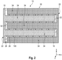
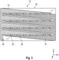
- Fig. 2 and 3 show variants of the Fig. 1 shown transparent displays 10.
- the same reference numerals denote the same elements as previously in Fig. 1 and a separate description is omitted below.
- Fig. 2 and 3 differ from Fig. 1 by arranging the light-emitting elements 100 in a matrix arrangement 30 and by a correspondingly modified structuring of the connection segments (first and second segments 16, 18).
- the matrix arrangement 30 comprises, for example, 4 rows and 8 columns with a total of 32 light-emitting components 100.
- the light-emitting components 100 are arranged in each row, as previously described with reference to Fig. 1 As indicated, they are connected in series via a plurality of segment sections 26. Additionally, a segment section 32 at the beginning and end of each row connects the individual rows to one another. This results in a continuous series connection of all light-emitting components 100 of the matrix arrangement 30.
- the first segment 16 connects all light-emitting components 100 to a first supply terminal 20, and the second segment 18 connects all light-emitting components 100 to a second supply terminal 22.
- the first segment 16 and the second segment 18 are comb-shaped and each have a segment section 34 per row.
- the segment sections 34 extend along the rows and alternately interlock.
- Fig. 2 and Fig. 3 differ in the design of the first and second segments 16, 18.
- the segment sections 34 of each row are each block-shaped and cover the largest possible area.
- Fig. 3 the segment sections 34, similar to the design according to Fig. 1 , are formed in a jagged shape and taper along the row. It goes without saying that the two configurations shown are only examples. Depending on the desired electrical properties of the supply line, a different structure for the first and second segments 16, 18 and their segment section 34 can be selected.
- the transparent displays 10 according to the Fig. 1 to 3 can be connected to a controller (not shown here) via the signal connection 28.
- the controller reads in display information and prepares it for display on the transparent display 10.
- the controller can be embodied as a microcontroller, FPGA, ASIC, DSP, or as a system on chip (SoC).
- SoC system on chip
- the controller can be implemented, for example, in the form of a Raspberry Pi or an
- the controller can read in image information and use it to determine brightness values for the individual light-emitting components 100.
- the controller then encodes the brightness values into a serial data stream and transmits this as a data signal to the light-emitting components 100.
- the brightness values for all light-emitting components 100 can be written sequentially into the serial data stream according to the arrangement of the light-emitting components 100 in the series circuit.
- Each light-emitting component 100 can extract and display the brightness value determined for itself from the data stream. In this way, the image read in by the controller can be displayed on the transparent display 10. It goes without saying that moving images can also be displayed by repeatedly performing this process.
- Fig. 4 shows a schematic representation of a single light-emitting component according to an embodiment of the present disclosure.
- the light-emitting component is designated in its entirety by reference numeral 100.
- the light-emitting component 100 is composed of individual components that can be arranged in a common housing 110.
- the individual components can be connected to one another, for example, on a common printed circuit board.
- the light-emitting component 100 has the four connections 102, 104, 106, 108 already described, via which the components arranged in the housing 110 can be contacted from the outside.
- the four connections include the two supply connections 102, 104, via which a supply voltage can be applied to the light-emitting component 100, and the signal connections 106, 108, via which a data signal can be received or output.
- the light-emitting component 100 further comprises at least one light-emitting device 112 and an integrated circuit 114.
- the light-emitting device 112 can comprise one or more controllable light-emitting diodes, the brightness of which can be controlled via the integrated circuit 114.
- the light-emitting device 112 can comprise three light-emitting diodes, each representing a primary color. By controlling the three light-emitting diodes 112 to different brightness values, the primary colors can be mixed to represent different colors.
- the integrated circuit 114 controls the light source 112 and adjusts it to different brightness values.
- the integrated circuit 114 obtains the brightness values from a data signal received at the signal terminal 106.
- the data signal can be a digital signal in which a bit sequence represents a brightness value for an individual LED.
- the integrated circuit 114 reads the brightness values for all LEDs of the light source 112 and controls the LEDs accordingly so that they display the transmitted brightness values.
- the light-emitting component 110 may further comprise a voltage regulator 116 which controls an electrical voltage provided at the supply terminals 102, 104 stabilized.
- the light-emitting component 112 and the integrated circuit 114 can be operated with the stabilized supply voltage.
- Voltage regulators are known in various variants, which can be based on different principles. The selection of a suitable voltage regulator can be crucial for error-free operation and can significantly influence energy efficiency.
- Other voltage regulators such as active DC-DC converters, can provide a constant supply voltage much more efficiently, but not at all, or only to a limited extent, with constant power consumption. While irregular power consumption, for example in the form of a pulsed current sink, may be unproblematic with a normal power supply, irregular power consumption with high lead resistances, as occurs in the transparent displays 10 described above, can be less efficient overall than constant power consumption, where excess power is converted into heat. Furthermore, fluctuating power consumption can also negatively impact data transmission between the light-emitting components and lead to transmission errors.
- the integrated circuit 114 can be designed to control the illuminant 112 in a defined manner and to enable a brightness change at a defined point in time. It has been shown that power fluctuations occur in particular when a illuminant changes from one brightness value to another. Because a defined point in time for the brightness change can be determined by the integrated circuit 114 and the integrated circuit 114 brings about the brightness change at the specific point in time, synchronization of a plurality of light-emitting components designed in this way components 100 and the performance fluctuations are limited to a defined period.
- the integrated circuit 114 can be configured to receive a serial data stream in which brightness values for a plurality of series-connected light-emitting components 100 are encoded, and to extract a brightness value for the illuminant 112 from the serial data stream. Based on the received serial data stream, the integrated circuit 114 can determine a switching time for controlling the illuminant 112 with the brightness value and set the illuminant 112 to the brightness value at the determined switching time. The process is described in detail with reference to the Fig. 5 explained in more detail.
- Fig. 5 shows a schematic representation of a functional structure 200 of an integrated circuit 114 of a light-emitting device 100 according to an embodiment of the present disclosure.
- the integrated circuit 114 is not limited to a particular form and may be, for example, a microcontroller, an ASIC, a DSP, an FPGA, or the like.
- the functional structure 200 is composed of several functional units which together implement the functions previously described with reference to Fig. 4
- the type of control of the light source described above can be implemented.
- the functional units comprise an input unit 202, an output unit 204, an error detection unit 206, a decoding unit 208, and a number of pulse width modulation units 210 corresponding to the number of LEDs 212 to be controlled.
- the input unit 202 is coupled to the signal terminal 106 of the light-emitting component 100 and can be configured as one or more serial interfaces.
- the input unit 202 receives the data signal present at the signal terminal 106.
- the data signal can be an electrical signal in which defined signal levels correspond to discrete values.
- the data signal can be a binary Data stream.
- the input unit 202 can, as shown here, have two redundant interfaces, wherein one interface is configured as a fallback interface and is alternatively switched on if no signal is received at the primary interface.
- the error detection unit 206 checks the data stream for errors and enables further processing if the data stream was received correctly. Further processing is performed by the decoding unit 208, which decodes the data stream and extracts the brightness information intended for the light-emitting component 100 from the data stream, for example, three brightness values with a length of 8 bits.
- the LEDs 212 are then controlled by the pulse-width modulation units 210, which convert the received brightness values into a pulse-width modulated signal and apply it to the LEDs 212.
- the data signal is output via the output unit 204 and made available to a subsequent light-emitting component 100.
- the functional units described above have already been implemented in this or a similar manner in known active light-emitting components, such as the Smart Pixel marketed under the designation WS2812B.
- the light-emitting component 100 according to the present disclosure differs from this, among other things, by a delay unit 214 and a delay time calculation unit 216.
- the delay unit 214 is configured to delay the brightness setting of the LEDs 212 for a defined period of time, for example, by preventing the transmission of new brightness values to the pulse width modulation units 210 until a defined time.
- the pulse width modulation units 210 thus provide the previous pulse width modulated signal until the defined period of time has elapsed, even if new brightness information has already been transmitted to the light-emitting component 100.
- the delay unit 214 can have a timer and a buffer.
- the brightness values for the defined period of time can be stored in the buffer.
- the timer can initiate further processing of the cached values at an adjustable time.
- the delay time calculation unit 216 is configured to determine the defined time period and provide a corresponding value, for example, to the timer. In other words, the delay time calculation unit 216 is configured to determine a switching time at which the light-emitting component 100 performs the brightness change of the illuminant 212. The calculation is performed based on the received data stream, for example, based on a value contained therein or advantageously also based on a length of the received data stream.
- the calculation is advantageously not tied to decoding the data stream.
- the number of subsequent light-emitting components can be determined based on the length of the data stream, and the determined number can be used to estimate when the last light-emitting component in the series circuit has received the data stream and is thus ready to switch the brightness values.
- it can be individually determined for each light-emitting component 100 when it must switch so that all light-emitting components 100 make the brightness change simultaneously.
- the estimation can be based on a known transmission delay of a light-emitting component 100 and under the assumption that the transmission delay is the same for all components or changes in a defined manner over time.
- Using the length of the data stream to determine the switching time also has the advantage that existing transmission protocols can be reused, since no additional data needs to be transmitted. Furthermore, common transmission protocols favor this method because the data is transmitted in a manner that facilitates estimation of the number of subsequent components. For example, common protocols first transmit the brightness information of the first light-emitting component and then that of the subsequent ones in descending order. Finally, the data stream terminated by a defined code word as a stop mark, e.g. a zero signal of a few microseconds.
- a light-emitting component 100 not only reads out its associated brightness information, but also removes it from the data stream and forwards the modified data stream to the subsequent components not only simplifies the reading of the data stream, since each component only has to read out the first information block of the data stream, but also the determination of an individual switching time, since the length of the data stream is individual at each component and corresponds to the actual length from the beginning of the data stream to the stop mark.
- the delay time calculation unit 216 can directly determine the number of subsequent components by dividing the length by the fixed length of a single brightness information block (e.g., 24 bits). The number can then be multiplied by a predefined time period t latency to calculate the individual delay time period and thus the switching instant at which the light-emitting component must switch in order to switch simultaneously with all other light-emitting components in the series circuit.
- the predefined time period t latency can, for example, be a transmission delay of the light-emitting component, which is preferably the same for all light-emitting components in the series circuit.
- undefined states can occur during a switching phase because the power consumption of the individual light-emitting components 100 changes, and this change is not compensated for or is compensated for only slowly when using energy-efficient DC-DC converters, as indicated here by reference numeral 218.
- Such an undefined state can lead to transmission errors and thus to faulty control of the light-emitting components 100.
- a blocking unit 220 can be provided, which blocks the digital inputs for the duration of the switching phase.
- the duration of the switching phase can be determined from an empirically determined value or derived from the previously determined number of light-emitting components 100 in the series circuit.
Landscapes
- Engineering & Computer Science (AREA)
- Physics & Mathematics (AREA)
- Computer Hardware Design (AREA)
- General Physics & Mathematics (AREA)
- Theoretical Computer Science (AREA)
- Control Of Indicators Other Than Cathode Ray Tubes (AREA)
Applications Claiming Priority (1)
| Application Number | Priority Date | Filing Date | Title |
|---|---|---|---|
| DE102023133436.0A DE102023133436B3 (de) | 2023-11-29 | 2023-11-29 | Lichtemittierendes Bauelement mit einem Leuchtmittel und einer integrierten Schaltung |
Publications (1)
| Publication Number | Publication Date |
|---|---|
| EP4564342A1 true EP4564342A1 (fr) | 2025-06-04 |
Family
ID=93704680
Family Applications (1)
| Application Number | Title | Priority Date | Filing Date |
|---|---|---|---|
| EP24215849.1A Withdrawn EP4564342A1 (fr) | 2023-11-29 | 2024-11-27 | Composant électroluminescent doté d'un moyen d'éclairage et d'un circuit intégré |
Country Status (2)
| Country | Link |
|---|---|
| EP (1) | EP4564342A1 (fr) |
| DE (1) | DE102023133436B3 (fr) |
Citations (6)
| Publication number | Priority date | Publication date | Assignee | Title |
|---|---|---|---|---|
| US8492983B1 (en) * | 2010-05-11 | 2013-07-23 | Analog Technologies Corporation | System and method to address and control serially connected LEDs |
| EP2879120A1 (fr) | 2012-07-18 | 2015-06-03 | G-Smatt Co., Ltd. | Panneau d'affichage électronique transparent et son procédé de fabrication |
| CN105873290A (zh) * | 2016-05-31 | 2016-08-17 | 深圳君略科技有限公司 | 一种led驱动芯片和led驱动电路 |
| DE102018107309A1 (de) | 2018-03-27 | 2019-10-02 | Symonics GmbH | Transparente Anzeigevorrichtung |
| DE212018000347U1 (de) * | 2018-01-31 | 2020-05-29 | Jiangsu Ledco Lighting Tech Co., Ltd | RGB synchron Smart-LED-Streifen |
| WO2021183299A1 (fr) * | 2020-03-11 | 2021-09-16 | Cree, Inc. | Commande active de diodes électroluminescentes et dispositifs d'affichage à diodes électroluminescentes |
-
2023
- 2023-11-29 DE DE102023133436.0A patent/DE102023133436B3/de active Active
-
2024
- 2024-11-27 EP EP24215849.1A patent/EP4564342A1/fr not_active Withdrawn
Patent Citations (6)
| Publication number | Priority date | Publication date | Assignee | Title |
|---|---|---|---|---|
| US8492983B1 (en) * | 2010-05-11 | 2013-07-23 | Analog Technologies Corporation | System and method to address and control serially connected LEDs |
| EP2879120A1 (fr) | 2012-07-18 | 2015-06-03 | G-Smatt Co., Ltd. | Panneau d'affichage électronique transparent et son procédé de fabrication |
| CN105873290A (zh) * | 2016-05-31 | 2016-08-17 | 深圳君略科技有限公司 | 一种led驱动芯片和led驱动电路 |
| DE212018000347U1 (de) * | 2018-01-31 | 2020-05-29 | Jiangsu Ledco Lighting Tech Co., Ltd | RGB synchron Smart-LED-Streifen |
| DE102018107309A1 (de) | 2018-03-27 | 2019-10-02 | Symonics GmbH | Transparente Anzeigevorrichtung |
| WO2021183299A1 (fr) * | 2020-03-11 | 2021-09-16 | Cree, Inc. | Commande active de diodes électroluminescentes et dispositifs d'affichage à diodes électroluminescentes |
Non-Patent Citations (1)
| Title |
|---|
| ANONYMOUS: "Intelligent control LED integrated light source. V1.0", WORLDSEMI CO., 1 January 2016 (2016-01-01), XP093234891, Retrieved from the Internet <URL:http://www.world-semi.com/#> [retrieved on 20250324] * |
Also Published As
| Publication number | Publication date |
|---|---|
| DE102023133436B3 (de) | 2025-03-20 |
Similar Documents
| Publication | Publication Date | Title |
|---|---|---|
| DE60008854T2 (de) | Led-matrix in gitterstruktur zur beleuchtung | |
| DE60008855T2 (de) | Dreidimensionale led matrix zur beleuchtung | |
| WO2001069978A1 (fr) | Commande de diodes electroluminescentes (led) | |
| DE202007011973U1 (de) | LED-Clusteranordnung mit Konstantstromschalter | |
| DE102009018428A1 (de) | Schaltung für eine Leuchtdiodenanordnung und Leuchtdiodenmodul | |
| DE102017109853A1 (de) | Halbleiter-Light Engine für eine Röhrenlampe | |
| DE102004043197A1 (de) | Verfahren zur Steuerung einer Beleuchtungsvorrichtung | |
| DE102023133436B3 (de) | Lichtemittierendes Bauelement mit einem Leuchtmittel und einer integrierten Schaltung | |
| DE112021006053B4 (de) | Treibervorrichtung für ein lichtemittierendes element | |
| DE2922595C2 (de) | Digitales Informationsübertragungssystem | |
| AT16808U1 (de) | Anordnung zur Beleuchtung | |
| DE102018107309B4 (de) | Transparente Anzeigevorrichtung | |
| DE102004044001A1 (de) | Verfahren zur Steuerung der Energiezufuhr von einer Stromquelle an einen Stromverbraucher | |
| EP1349434A2 (fr) | Circuit d'éclairage, en particulier pour voitures | |
| EP1463654A1 (fr) | Plaque | |
| WO1999038361A1 (fr) | Circuit servant a faire fonctionner un signal lumineux a diodes electroluminescentes | |
| DE2902941A1 (de) | Sichtanzeigeeinrichtung | |
| EP2217040B1 (fr) | Dispositif d'affichage, procédé de fonctionnement et dispositif d'éclairage | |
| EP3506723B1 (fr) | Convertisseur à découpage permettant d'alimenter un montage en série composé de diodes électroluminescentes | |
| EP3866568B1 (fr) | Bande led | |
| EP1937042A2 (fr) | Système de liaison pour un module d'affichage | |
| DE102019217344A1 (de) | Beleuchtungsmodule mit einem schaltungsträger und lichtquellen | |
| DE112012005777T5 (de) | Verfahren und Vorrichtung zum Antrieb von LED basierten Beleuchtungseinheiten | |
| DE202024104755U1 (de) | LED-System mit schaltbaren Lichtszenen | |
| DE102018121451B3 (de) | LED-Lichtband und Leuchtsystem |
Legal Events
| Date | Code | Title | Description |
|---|---|---|---|
| PUAI | Public reference made under article 153(3) epc to a published international application that has entered the european phase |
Free format text: ORIGINAL CODE: 0009012 |
|
| STAA | Information on the status of an ep patent application or granted ep patent |
Free format text: STATUS: THE APPLICATION HAS BEEN PUBLISHED |
|
| AK | Designated contracting states |
Kind code of ref document: A1 Designated state(s): AL AT BE BG CH CY CZ DE DK EE ES FI FR GB GR HR HU IE IS IT LI LT LU LV MC ME MK MT NL NO PL PT RO RS SE SI SK SM TR |
|
| STAA | Information on the status of an ep patent application or granted ep patent |
Free format text: STATUS: THE APPLICATION IS DEEMED TO BE WITHDRAWN |
|
| 18D | Application deemed to be withdrawn |
Effective date: 20251205 |