EP4128337B1 - Module de puissance pourvu d'au moins trois unités de puissance - Google Patents
Module de puissance pourvu d'au moins trois unités de puissance Download PDFInfo
- Publication number
- EP4128337B1 EP4128337B1 EP21725434.1A EP21725434A EP4128337B1 EP 4128337 B1 EP4128337 B1 EP 4128337B1 EP 21725434 A EP21725434 A EP 21725434A EP 4128337 B1 EP4128337 B1 EP 4128337B1
- Authority
- EP
- European Patent Office
- Prior art keywords
- power
- power module
- heat sink
- units
- coolant flow
- Prior art date
- Legal status (The legal status is an assumption and is not a legal conclusion. Google has not performed a legal analysis and makes no representation as to the accuracy of the status listed.)
- Active
Links
Images


Classifications
-
- H—ELECTRICITY
- H10—SEMICONDUCTOR DEVICES; ELECTRIC SOLID-STATE DEVICES NOT OTHERWISE PROVIDED FOR
- H10W—GENERIC PACKAGES, INTERCONNECTIONS, CONNECTORS OR OTHER CONSTRUCTIONAL DETAILS OF DEVICES COVERED BY CLASS H10
- H10W90/00—Package configurations
-
- H—ELECTRICITY
- H05—ELECTRIC TECHNIQUES NOT OTHERWISE PROVIDED FOR
- H05K—PRINTED CIRCUITS; CASINGS OR CONSTRUCTIONAL DETAILS OF ELECTRIC APPARATUS; MANUFACTURE OF ASSEMBLAGES OF ELECTRICAL COMPONENTS
- H05K7/00—Constructional details common to different types of electric apparatus
- H05K7/20—Modifications to facilitate cooling, ventilating, or heating
- H05K7/2089—Modifications to facilitate cooling, ventilating, or heating for power electronics, e.g. for inverters for controlling motor
- H05K7/20909—Forced ventilation, e.g. on heat dissipaters coupled to components
- H05K7/20918—Forced ventilation, e.g. on heat dissipaters coupled to components the components being isolated from air flow, e.g. hollow heat sinks, wind tunnels or funnels
-
- H—ELECTRICITY
- H10—SEMICONDUCTOR DEVICES; ELECTRIC SOLID-STATE DEVICES NOT OTHERWISE PROVIDED FOR
- H10W—GENERIC PACKAGES, INTERCONNECTIONS, CONNECTORS OR OTHER CONSTRUCTIONAL DETAILS OF DEVICES COVERED BY CLASS H10
- H10W40/00—Arrangements for thermal protection or thermal control
- H10W40/01—Manufacture or treatment
- H10W40/03—Manufacture or treatment of arrangements for cooling
- H10W40/037—Assembling together parts thereof
-
- H—ELECTRICITY
- H10—SEMICONDUCTOR DEVICES; ELECTRIC SOLID-STATE DEVICES NOT OTHERWISE PROVIDED FOR
- H10W—GENERIC PACKAGES, INTERCONNECTIONS, CONNECTORS OR OTHER CONSTRUCTIONAL DETAILS OF DEVICES COVERED BY CLASS H10
- H10W40/00—Arrangements for thermal protection or thermal control
- H10W40/20—Arrangements for cooling
- H10W40/22—Arrangements for cooling characterised by their shape, e.g. having conical or cylindrical projections
- H10W40/226—Arrangements for cooling characterised by their shape, e.g. having conical or cylindrical projections characterised by projecting parts, e.g. fins to increase surface area
-
- H—ELECTRICITY
- H10—SEMICONDUCTOR DEVICES; ELECTRIC SOLID-STATE DEVICES NOT OTHERWISE PROVIDED FOR
- H10W—GENERIC PACKAGES, INTERCONNECTIONS, CONNECTORS OR OTHER CONSTRUCTIONAL DETAILS OF DEVICES COVERED BY CLASS H10
- H10W40/00—Arrangements for thermal protection or thermal control
- H10W40/40—Arrangements for thermal protection or thermal control involving heat exchange by flowing fluids
- H10W40/43—Arrangements for thermal protection or thermal control involving heat exchange by flowing fluids by flowing gases, e.g. forced air cooling
-
- H—ELECTRICITY
- H10—SEMICONDUCTOR DEVICES; ELECTRIC SOLID-STATE DEVICES NOT OTHERWISE PROVIDED FOR
- H10W—GENERIC PACKAGES, INTERCONNECTIONS, CONNECTORS OR OTHER CONSTRUCTIONAL DETAILS OF DEVICES COVERED BY CLASS H10
- H10W70/00—Package substrates; Interposers; Redistribution layers [RDL]
- H10W70/60—Insulating or insulated package substrates; Interposers; Redistribution layers
- H10W70/611—Insulating or insulated package substrates; Interposers; Redistribution layers for connecting multiple chips together
-
- H—ELECTRICITY
- H10—SEMICONDUCTOR DEVICES; ELECTRIC SOLID-STATE DEVICES NOT OTHERWISE PROVIDED FOR
- H10W—GENERIC PACKAGES, INTERCONNECTIONS, CONNECTORS OR OTHER CONSTRUCTIONAL DETAILS OF DEVICES COVERED BY CLASS H10
- H10W90/00—Package configurations
- H10W90/401—Package configurations characterised by multiple insulating or insulated package substrates, interposers or RDLs
-
- H—ELECTRICITY
- H10—SEMICONDUCTOR DEVICES; ELECTRIC SOLID-STATE DEVICES NOT OTHERWISE PROVIDED FOR
- H10W—GENERIC PACKAGES, INTERCONNECTIONS, CONNECTORS OR OTHER CONSTRUCTIONAL DETAILS OF DEVICES COVERED BY CLASS H10
- H10W90/00—Package configurations
- H10W90/701—Package configurations characterised by the relative positions of pads or connectors relative to package parts
-
- H—ELECTRICITY
- H10—SEMICONDUCTOR DEVICES; ELECTRIC SOLID-STATE DEVICES NOT OTHERWISE PROVIDED FOR
- H10W—GENERIC PACKAGES, INTERCONNECTIONS, CONNECTORS OR OTHER CONSTRUCTIONAL DETAILS OF DEVICES COVERED BY CLASS H10
- H10W40/00—Arrangements for thermal protection or thermal control
- H10W40/20—Arrangements for cooling
- H10W40/25—Arrangements for cooling characterised by their materials
- H10W40/255—Arrangements for cooling characterised by their materials having a laminate or multilayered structure, e.g. direct bond copper [DBC] ceramic substrates
-
- H—ELECTRICITY
- H10—SEMICONDUCTOR DEVICES; ELECTRIC SOLID-STATE DEVICES NOT OTHERWISE PROVIDED FOR
- H10W—GENERIC PACKAGES, INTERCONNECTIONS, CONNECTORS OR OTHER CONSTRUCTIONAL DETAILS OF DEVICES COVERED BY CLASS H10
- H10W72/00—Interconnections or connectors in packages
- H10W72/071—Connecting or disconnecting
- H10W72/073—Connecting or disconnecting of die-attach connectors
- H10W72/07331—Connecting techniques
-
- H—ELECTRICITY
- H10—SEMICONDUCTOR DEVICES; ELECTRIC SOLID-STATE DEVICES NOT OTHERWISE PROVIDED FOR
- H10W—GENERIC PACKAGES, INTERCONNECTIONS, CONNECTORS OR OTHER CONSTRUCTIONAL DETAILS OF DEVICES COVERED BY CLASS H10
- H10W72/00—Interconnections or connectors in packages
- H10W72/30—Die-attach connectors
- H10W72/351—Materials of die-attach connectors
- H10W72/352—Materials of die-attach connectors comprising metals or metalloids, e.g. solders
-
- H—ELECTRICITY
- H10—SEMICONDUCTOR DEVICES; ELECTRIC SOLID-STATE DEVICES NOT OTHERWISE PROVIDED FOR
- H10W—GENERIC PACKAGES, INTERCONNECTIONS, CONNECTORS OR OTHER CONSTRUCTIONAL DETAILS OF DEVICES COVERED BY CLASS H10
- H10W72/00—Interconnections or connectors in packages
- H10W72/30—Die-attach connectors
- H10W72/351—Materials of die-attach connectors
- H10W72/353—Materials of die-attach connectors not comprising solid metals or solid metalloids, e.g. ceramics
- H10W72/354—Materials of die-attach connectors not comprising solid metals or solid metalloids, e.g. ceramics comprising polymers
-
- H—ELECTRICITY
- H10—SEMICONDUCTOR DEVICES; ELECTRIC SOLID-STATE DEVICES NOT OTHERWISE PROVIDED FOR
- H10W—GENERIC PACKAGES, INTERCONNECTIONS, CONNECTORS OR OTHER CONSTRUCTIONAL DETAILS OF DEVICES COVERED BY CLASS H10
- H10W72/00—Interconnections or connectors in packages
- H10W72/50—Bond wires
- H10W72/531—Shapes of wire connectors
- H10W72/533—Cross-sectional shape
- H10W72/534—Cross-sectional shape being rectangular
-
- H—ELECTRICITY
- H10—SEMICONDUCTOR DEVICES; ELECTRIC SOLID-STATE DEVICES NOT OTHERWISE PROVIDED FOR
- H10W—GENERIC PACKAGES, INTERCONNECTIONS, CONNECTORS OR OTHER CONSTRUCTIONAL DETAILS OF DEVICES COVERED BY CLASS H10
- H10W72/00—Interconnections or connectors in packages
- H10W72/50—Bond wires
- H10W72/551—Materials of bond wires
-
- H—ELECTRICITY
- H10—SEMICONDUCTOR DEVICES; ELECTRIC SOLID-STATE DEVICES NOT OTHERWISE PROVIDED FOR
- H10W—GENERIC PACKAGES, INTERCONNECTIONS, CONNECTORS OR OTHER CONSTRUCTIONAL DETAILS OF DEVICES COVERED BY CLASS H10
- H10W72/00—Interconnections or connectors in packages
- H10W72/851—Dispositions of multiple connectors or interconnections
- H10W72/874—On different surfaces
- H10W72/884—Die-attach connectors and bond wires
-
- H—ELECTRICITY
- H10—SEMICONDUCTOR DEVICES; ELECTRIC SOLID-STATE DEVICES NOT OTHERWISE PROVIDED FOR
- H10W—GENERIC PACKAGES, INTERCONNECTIONS, CONNECTORS OR OTHER CONSTRUCTIONAL DETAILS OF DEVICES COVERED BY CLASS H10
- H10W72/00—Interconnections or connectors in packages
- H10W72/90—Bond pads, in general
- H10W72/941—Dispositions of bond pads
- H10W72/944—Dispositions of multiple bond pads
-
- H—ELECTRICITY
- H10—SEMICONDUCTOR DEVICES; ELECTRIC SOLID-STATE DEVICES NOT OTHERWISE PROVIDED FOR
- H10W—GENERIC PACKAGES, INTERCONNECTIONS, CONNECTORS OR OTHER CONSTRUCTIONAL DETAILS OF DEVICES COVERED BY CLASS H10
- H10W90/00—Package configurations
- H10W90/701—Package configurations characterised by the relative positions of pads or connectors relative to package parts
- H10W90/731—Package configurations characterised by the relative positions of pads or connectors relative to package parts of die-attach connectors
- H10W90/734—Package configurations characterised by the relative positions of pads or connectors relative to package parts of die-attach connectors between a chip and a stacked insulating package substrate, interposer or RDL
-
- H—ELECTRICITY
- H10—SEMICONDUCTOR DEVICES; ELECTRIC SOLID-STATE DEVICES NOT OTHERWISE PROVIDED FOR
- H10W—GENERIC PACKAGES, INTERCONNECTIONS, CONNECTORS OR OTHER CONSTRUCTIONAL DETAILS OF DEVICES COVERED BY CLASS H10
- H10W90/00—Package configurations
- H10W90/701—Package configurations characterised by the relative positions of pads or connectors relative to package parts
- H10W90/751—Package configurations characterised by the relative positions of pads or connectors relative to package parts of bond wires
- H10W90/754—Package configurations characterised by the relative positions of pads or connectors relative to package parts of bond wires between a chip and a stacked insulating package substrate, interposer or RDL
-
- H—ELECTRICITY
- H10—SEMICONDUCTOR DEVICES; ELECTRIC SOLID-STATE DEVICES NOT OTHERWISE PROVIDED FOR
- H10W—GENERIC PACKAGES, INTERCONNECTIONS, CONNECTORS OR OTHER CONSTRUCTIONAL DETAILS OF DEVICES COVERED BY CLASS H10
- H10W90/00—Package configurations
- H10W90/701—Package configurations characterised by the relative positions of pads or connectors relative to package parts
- H10W90/761—Package configurations characterised by the relative positions of pads or connectors relative to package parts of strap connectors
- H10W90/764—Package configurations characterised by the relative positions of pads or connectors relative to package parts of strap connectors between a chip and a stacked insulating package substrate, interposer or RDL
Definitions
- the invention relates to a power module with at least three power units.
- the invention relates to a power converter with at least one such power semiconductor module.
- switch modules that are closed, in particular by a housing, and are currently manufactured in discrete designs, for example via a solid metallic base plate, are screwed onto a heat sink.
- a power converter is understood to mean, for example, a rectifier, an inverter, a converter or a DC-DC converter.
- the disclosure document DE 10 2009 001 722 A1 describes a power semiconductor module, the base plate of which is designed as a multi-layer substrate and is provided with a hardened thermal paste, and which is brought into thermal contact with a heat sink.
- the disclosure document DE 10 2010 022 562 A1 describes an electrical power module for mounting on a circuit board, comprising a first side for mounting on a surface of a heat sink, the first side being arranged substantially parallel to the heat sink in a mounted position of the electrical power module on the heat sink, and one provided with electrical connection elements second side, wherein the electrical connecting elements are adapted to electrically connect the electrical power module to the circuit board.
- the electrical power module can be connected to the circuit board and the heat sink in a simpler manner if the electrical power module includes or is adapted to at least one dowel-like fastening element which is insertable into at least one bore of the heat sink and is adapted to accommodate a clamping element such that the clamping element clamps in the at least one bore of the heat sink by its insertion into the at least one dowel-like fastening element.
- EP 3 624 184 A1 describes a method for producing a power module unit, in which a base plate is provided with recesses.
- the base plate is connected to a substrate that carries the power semiconductor. After the substrate has been attached to the base plate, the cooling fins are guided into the recesses in the base plate and fastened in a form-fitting and/or force-fitting manner.
- the patent specification DE 10 2008 007 310 B4 describes an electrical press-fit contact, in particular press-in pin contact, for transmitting electrical current and / or electrical signals, with a press-in section and a mounting section, which are mechanically coupled to one another via a relief section, and the relief section has a compensation area and a stop area, the compensation area having a coupled allows relative movement of the press-in section and the mounting section, and the stop region blocks a movement of the press-in section and the mounting section towards one another, and wherein the stop region of the relief section is arranged symmetrically with respect to a force center line of the electrical press-in contact, along which a press-in force can be introduced into the electrical press-in contact, which results from a press-in of the electrical press-fit contact into a carrier.
- Conductor traces define power buses for a switching topology, e.g. with GaN E-HEMTs, where the power connectors extend from the power buses through the package to provide a heatsink to busbar clearance that meets creepage and airflow requirements.
- the WO 2007/065666 A2 describes an electrical device comprising heat-generating electrical components, in particular power semiconductors, and a cooling device for dissipating this heat, the cooling device being formed from an air cooler to which a liquid cooler is mounted, the air cooler being provided between the liquid cooler and the heat-generating electrical components is.
- EP 3 273 471 A1 describes a power module with at least three power units, each of which has at least one power semiconductor and a substrate connected to a surface of a common heat sink, wherein the heat sink is configured such that a gaseous coolant flows in a coolant flow direction, wherein the coolant flow direction runs substantially parallel to the surface of the heat sink , wherein the power units are arranged offset transversely to the coolant flow direction.
- a power module with at least three power units, each of which comprises at least one power semiconductor and a substrate, the at least one power semiconductor being connected, in particular materially, to the respective substrate, the substrates of the at least three power units each being directly materially connected are connected to a surface of a common heat sink, the heat sink being configured such that a gaseous coolant flows in a coolant flow direction, the coolant flow direction being substantially parallel to the surface of the heat sink, wherein the power units are arranged offset transversely to the coolant flow direction, wherein the heat sink has cooling fins arranged running in a coolant flow direction, wherein a power board arranged substantially parallel to the surface of the heat sink is connected to the power units via freely positionable contacts.
- the object is achieved according to the invention by a power converter with at least one such power module.
- the invention is based on the idea of reducing the space required by a power module by reducing the number of thermal interfaces and thereby achieving improved heat dissipation.
- a power module has at least three power units, the power units each comprising at least one power semiconductor and a substrate.
- a substrate is a dielectric material layer metallized on both sides, the dielectric material layer having, for example, a thickness d of 25 ⁇ m to 400 ⁇ m, in particular 50 ⁇ m to 250 ⁇ m.
- the dielectric material layer contains a ceramic material, for example aluminum nitride or aluminum oxide, or an organic material, for example a polyamide.
- the metallization contains copper, molybdenum, gold and/or silver.
- the power semiconductor is in particular designed as a transistor and/or a diode, the transistor being designed, for example, as an insulated gate bipolar transistor (IGBT), as a metal oxide semiconductor field effect transistor (MOSFET) or as a field effect transistor .
- the at least one power semiconductor is connected to the respective substrate, in particular in a materially bonded manner, for example via a sintered connection or soldered connection.
- the substrates of the power units are each directly connected in a materially bonded manner to a surface of a common heat sink, in particular with a side facing away from the at least one power semiconductor.
- Direct material contact means direct contact
- connecting means for producing the cohesive connection such as glue, solder, sintering paste, ...
- an additional connecting element such as an additional conductor, a bonding wire, a spacer, a base plate, thermal paste, ...
- a cohesive connection of at least three power units on a common heat sink results in a high degree of flexibility with regard to the positioning of the power units on the surface of the heat sink in order to achieve optimized heat dissipation through heat spreading and to make maximum use of the surface of the heat sink.
- the heat sink is configured such that a gaseous coolant flows in a coolant flow direction, the coolant flow direction being substantially parallel to the surface of the heat sink.
- the gaseous coolant is, for example, air.
- the power module is cooled on one side by a fan which is in fluid communication with the cooling fins of the heat sink, so that the air from the fan flows over the cooling fins of the heat sink essentially parallel to the surface of the heat sink.
- the at least three power units are arranged offset transversely to the coolant flow direction.
- a staggered arrangement achieves heat spreading, which leads to optimal heat dissipation.
- a power board is to be understood as meaning a printed circuit board, which is designed, for example, as a printed circuit board (PCB), in particular with multiple layers.
- the circuit board contains, for example, an interface to the power units, a driver circuit, a control circuit, and/or capacitors.
- a freely positionable contact means for example, a pin that can be freely arranged on a substrate due to its structural properties. Such structural properties are, for example, a foot that allows the pin, for example through a cohesive connection to the substrate, to be freely and stably arranged on the substrate without a housing or other stabilizing means and/or a swash circle that allows a hole to be found in the power board and ensures more stability and robustness, for example in the event of thermal expansion during operation.
- Such a contact is made, for example, from copper or a copper alloy in order to achieve low resistance and high current-carrying capacity.
- the free positioning of the contacts results in short cable paths and the associated low inductances, which enables power units with low impedances and low losses.
- a cell-specific design of the power units is made possible inexpensively and easily.
- the substrates of the power units each have a dielectric material layer with a thermal conductivity of at least 25 Wm -1 .K -1 , in particular at least 100 Wm -1 .K -1 , and a thickness of 25 ⁇ m to 400 ⁇ m, in particular 50 ⁇ m to 250 ⁇ m.
- the dielectric material layer is made of aluminum nitride or aluminum oxide.
- the use of such thin ceramic layers is made possible by the multiple substrates that are cohesively connected to the heat sink surface, which leads to an improvement in the thermal connection of the power semiconductors.
- a further embodiment provides that at least two of the power units have a common housing.
- a common housing is made, for example, from a plastic.
- the common housing saves installation space.
- a further embodiment provides that at least two of the power units are connected to one another in an electrically conductive manner, in particular via a bond connection.
- a bond connection is made, for example, using bonding wires or ribbon bonds.
- identical power units can be connected in parallel via the bond connection in order to drive a higher load current.
- power modules can be manufactured in a cost-effective, scalable manner.
- a further embodiment provides that the heat sink, which is made from a first metallic material, has on its surface at least one cavity which is filled with a second metallic material which has a higher thermal conductivity than the first metallic material, wherein at least one Substrate of a power unit is directly materially connected to the second metallic material.
- the first metallic material is aluminum and the second metallic material is copper.
- An improved thermal connection of the power units to the heat sink is achieved through a cavity filled with the second metallic material.
- a further embodiment provides that the second metallic material is essentially flush with the surface of the heat sink.
- a finish that is flush with the surface of the heat sink is to be understood as meaning a flat finish to the filling of the cavity that is essentially continuous with the heat sink surface.
- the second metallic material forms a flat surface that is essentially seamless into the heat sink surface transforms. Such a flat design achieves an optimal thermal connection to the heat sink and avoids mechanical and/or thermal stresses in the substrate connected to the second metallic material.
- each of the at least two power units is assigned a cavity filled with the second metallic material.
- the cavities filled with the second metallic material are, for example, designed as islands that have a larger area than the respective substrates and protrude beyond the substrate on each of the substrate edges, whereby an improved thermal connection of the power units to the heat sink is achieved.
- a further embodiment provides that the second metallic material is introduced into the at least one cavity using an additive process.
- the second metallic material is introduced into the at least one cavity by means of cold gas spraying.
- the additive process allows, especially in comparison to a casting process, a very low thickness of the first metallic material below the cavity, so that the cooling fins are very close to the second metallic material, which has a higher thermal conductivity than the first metallic material, so that a improved thermal connection to a cooling fluid is achieved.
- a further embodiment provides that the power units are arranged on the surface of the heat sink in such a way that optimal heat dissipation of the power semiconductors takes place through heat spreading.
- the power units are oriented and spaced on the heat sink, in particular in relation to a flow direction of a coolant, so that the waste heat generated in the power semiconductors of the power units, in particular approximately at certain points, is distributed as evenly as possible on the surface of the Heat sink is distributed and so heat spread takes place.
- Such an arrangement achieves greater robustness of the power module during operation.
- a further embodiment provides that a distance between the power units varies in the coolant flow direction and/or transversely to the coolant flow direction.
- one power unit is assigned to one phase of a three-phase system.
- a further embodiment provides that a distance between the power units increases in the coolant flow direction. Since the coolant heats up in the coolant flow direction below the power units, increasing distance results in better mixing of strongly and weakly heated coolant. Furthermore, at least a higher cooling rate is achieved with increasing distance, so that increasing distances in the coolant flow direction lead to a more uniform temperature distribution on the heat sink.
- a further embodiment provides that the freely positionable contacts are cohesively connected to the respective substrates of the power units.
- the freely positionable contacts are soldered onto the respective substrates and connected to the power board using a press-fit connection.
- a further embodiment provides that the freely positionable contacts are designed asymmetrically with respect to a force center line.
- a press-in force can be introduced into the freely positionable contact along the force center line.
- a further embodiment provides that the heat sink is made from an aluminum alloy with a silicon content of up to 1.0%, in particular up to 0.6%, by means of extrusion.
- an extruded heat sink achieves improved thermal conductivity because a low silicon content can be used during extrusion.
- An extruded heat sink made from such an aluminum alloy leads to improved heat spreading.
- a further embodiment provides that the cooling fins are arranged in such a way that a ratio of a length of the cooling fins to a distance between the cooling fins is at least 10.
- a ratio can be achieved, for example, by extrusion, with optimal heat dissipation being achieved, particularly with an extruded heat sink.
- short cooling fins for example with a length of 20 mm to 30 mm, are made possible, so that the power module with the heat sink can be processed in a soldering oven, in particular in an automated manner, which makes the production of the power module simpler and more cost-effective.
- the heat sink has a base plate with a substantially constant first thickness of 3.5 mm to 5 mm, in particular 3.5 mm to 4 mm, wherein the base plate and the cooling fins of the heat sink are made in one piece.
- a thin base plate which can be produced, for example, by extrusion, leads to improved heat dissipation.
- such a thin base plate reduces the overall height of the power module, so that the power module can be processed with the heat sink in a soldering oven, in particular in an automated manner is, which makes the production of the power module easier and cheaper.
- the described components of the embodiments each represent individual features of the invention that can be viewed independently of one another
- the invention can also be further developed independently of each other and can therefore also be viewed as part of the invention individually or in a combination other than that shown.
- the described embodiments can also be supplemented by further features of the invention that have already been described.
- FIG 1 shows a schematic representation of a first embodiment of a power module 2 in cross section.
- the power module 2 has, for example, two power units 4, each of which includes power semiconductors 6 and a substrate 8.
- the power semiconductors 6 are designed as a transistor 10 or as a diode 12, with the transistor 10 being designed, for example, as an insulated gate bipolar transistor (IGBT), as a metal oxide semiconductor field effect transistor (MOSFET) or as a field effect transistor.
- IGBT insulated gate bipolar transistor
- MOSFET metal oxide semiconductor field effect transistor
- each of the transistors 10 is assigned a diode 12, in particular an antiparallel one.
- the substrates 8 of the two power units 4 have a dielectric material layer 14 which contains a ceramic material, for example aluminum nitride or aluminum oxide, or an organic material, for example a polyamide.
- the dielectric material layer 14 has a thickness d of 25 ⁇ m to 400 ⁇ m, in particular 50 ⁇ m to 250 ⁇ m.
- the substrates 8 each have an, in particular structured, upper metallization 18 on a side 16 facing the power semiconductors 6 and a lower metallization 22 on a side 20 facing away from the power semiconductors 6, the substrates 8 each being directly cohesively bonded to a surface 24 common heat sink 26 are connected.
- the upper metallization 18 and the lower metallization 22 are made of copper, for example.
- the cohesive connection 28 to the heat sink 26 is produced by soldering or sintering.
- a direct cohesive contact is to be understood as a direct contact that includes connecting means for producing the cohesive connection such as glue, solder, sintering paste, ..., an additional connecting element such as an additional conductor, a bonding wire, a spacer, a base plate, thermal paste, . .. but excludes.
- a side 30 of the power semiconductors 6 facing the substrate 8 is also connected to the upper metallization 18 of the substrate 8 via a cohesive connection 28, which is produced by soldering or sintering.
- a side 32 of the power semiconductors 6 facing away from the substrate 8 is each connected to the upper metallization 18 of the substrate 8 via a bond connection 34.
- the bond connection 34 includes, for example, at least one bonding wire, at least one ribbon bond and/or other means for producing a bond connection.
- the transistors 10 in FIG 1 are designed, for example, as IGBTs, the collector contact C of which is connected to the upper metallization 18 of the substrate 8 on the side 30 of the power semiconductor 6 facing the substrate 8 via a cohesive connection 28.
- the emitter contacts E of the transistors 10 designed as IGBTs are electrically insulated from them and connected to the upper metallization 18 of the substrate 8 via bond connections 34.
- the gate contacts of the transistors 10 and the bond connections of the diodes 12 are shown for clarity FIG 1 not shown.
- a power board 36 arranged essentially parallel to the surface 24 of the heat sink 26 is connected to the power units 4 via freely positionable contacts 38, the freely positionable contacts 38 being connected in a materially bonded manner to the upper metallizations 18 of the respective substrates 8 of the power units 4.
- the freely positionable contacts 38 have an elastically yielding section and are connected to the power board 36, for example with a press-fit connection.
- the heat sink 26 is made of a first metallic material 39. On its surface 24, cavities 40 are introduced which are filled with a second metallic material 42, the second metallic material 42 having a higher thermal conductivity than the first metallic material 39.
- the first metallic material 39 is aluminum and the second metallic material 42 is copper.
- Each of the at least two power units 4 is assigned a cavity 40 filled with the second metallic material 42, the second metallic material 42 being essentially flush with the surface 24 of the heat sink 26 and the lower metallizations 22 of the respective substrate 8 cohesively with the second metallic Material 42 are connected.
- the second metallic material 42 is introduced into the cavities using an additive process, for example using cold gas spraying.
- Each of the power units 4 can be assigned a dedicated sensor, in particular a temperature sensor, in order to monitor the temperature of the power semiconductors 6.
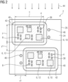
- FIG 2 shows a schematic representation of a second embodiment of a power module 2 in a top view.
- the heat sink 26 is configured, for example by cooling fins, for a gaseous coolant to flow in a coolant flow direction 44, wherein the coolant flow direction 44 runs substantially parallel to the surface 24 of the heat sink 26.
- the gaseous coolant is, for example, air which flows via a fan in the coolant flow direction 44 over the cooling fins of the heat sink 26.
- the power module 2 has, for example, two power units 4, which are spaced apart on the surface 24 of the heat sink 26 in such a way that optimal heat dissipation of the power semiconductors 6 takes place through heat spreading.
- the power units 4 have a rectangular base area with identical dimensions x, y.
- the power units 4 viewed transversely to the coolant flow direction 44, are arranged offset by a first transverse offset x1.
- the power units 4, viewed in the coolant flow direction 44 are spaced apart by a longitudinal offset y1. Due to the size of the surface 24 of the heat sink 26, the transverse offset x1 and the longitudinal offset y1 are smaller than the respective dimensions x, y of the power unit 4. Due to the cohesive connection of the power units 4 to the heat sink 26, fewer assembly points 46 are required.
- each power unit 4 is assigned two mounting points 46, with the heat sink 26 having at least two mounting points 46, in particular at least four mounting points 46.
- the further version of the power module 2 in FIG 2 corresponds to the version in FIG 1 .
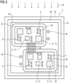
- FIG 3 shows a schematic representation of a third embodiment of a power module 2 in a top view, the two power units 4 having a common housing 48.
- the two power units 4 of the power module 2 are electrically connected to one another via a bond connection 34, the bond connection 34 having a plurality of bonding wires, ribbon bonds and/or other means for producing the bond connection 34.
- the housing 48 includes a half-bridge circuit for high-current applications, with two half-bridges, each associated with a power unit 4, being connected in parallel to drive a higher load current.
- the further version of the power module 2 in FIG 3 corresponds to the version in FIG 2 .
- FIG 4 shows a schematic representation of a fourth embodiment of a power module 2 in a top view, wherein the power module 2 includes three power units 4.
- a distance x1, x2, y1, y2 between the power units 4 varies in the coolant flow direction 44 and transversely to the coolant flow direction 44.
- These are arranged in such a way that the distance y1, y2 between the power units 4 increases in the coolant flow direction 44.
- the further version of the power module 2 in FIG 3 corresponds to the version in FIG 2 .
- FIG 5 shows a schematic representation of a fifth embodiment of a power module 2 in a top view, in which, in addition to the variation of the distances x1, x2, y1, y2 between the power units 4, additional heat spreading is achieved by different arrangements of the components on the substrates 8.
- the power semiconductors 6 with the freely positionable contacts 38 are arranged on the respective substrates in such a way that optimal heat dissipation of the power semiconductors 4 takes place.
- the area of the respective substrates 8 can be varied for greater heat spread.
- the further version of the power module 2 in FIG 5 corresponds to the version in FIG 4 .
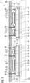
- FIG 6 shows a schematic three-dimensional representation of a sixth embodiment of a power module 2, wherein the power module 2 comprises three power units 4.
- the power units 4 each have a housing 48 with a housing cover 50, the housing cover 50 being shown transparently in the front power unit 4.
- the heat sink has a base plate 51 with cooling fins 52 arranged running in the coolant flow direction 44, the cooling fins 52 being connected to the base plate 51 and the base plate 51 and the cooling fins 52 of the heat sink 26 being made in one piece.
- the base plate 51 has a substantially constant first thickness d1 of 3.5 mm to 5 mm, in particular 3.5 mm to 4 mm, while the ribs have a second thickness d2, which is smaller than the first thickness d1 of the base plate 51 is.
- the cooling fins 52 are arranged equidistantly transversely to the coolant flow direction 44.
- the heat sink 26 is made by extrusion from an aluminum alloy, which contains, for example, silicon from 0.1% to 1.0%, in particular from 0.1% to 0.6%. Furthermore, the cooling fins 52 are arranged such that a ratio of a length l of the cooling fins 52 to a distance a between the cooling fins 52 is at least 10: l/a ⁇ 10.
- the further version of the power module 2 in FIG 6 corresponds to the version in FIG 4 .
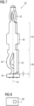
- FIG 7 shows a three-dimensional representation of a freely positionable contact 38.
- the freely positionable contact 38 has a press-in zone 53, which can be connected to the power board 36 and is designed asymmetrically with respect to a force center line 54, with a press-in force in the force center line 54 freely positionable contact 38 can be initiated.
- Positioning aids 56 for aligning the freely positionable contact 38 for example in a soldering jig, are mounted in a central part 55.
- a lower part 58 of the freely positionable contact 38 is designed as an asymmetrical relief section which has an elastically yielding section 60 and a stop 62 arranged parallel thereto, the stop being spaced from a foot 64 by a gap width s.
- the foot 64 is configured for a cohesive connection, for example by soldering or sintering.
- the freely positionable contact 38 is materially connected to the upper metallization 18 of a substrate 8 via the foot 64.
- the elastically yielding section 60 has an S-shaped spring shape with a defined spring travel. In this way, forces occurring during the press-in process or during operation, which are caused, for example, by vibrations, can be absorbed in the relief section. In addition, tolerances can be compensated for due to the elasticity. In particular, a spring constant of the elastically yielding section 60 is produced with the aid of a cross-sectional reduction by punching.
- the further version of the freely positionable contact 38 in FIG 7 corresponds to the version in FIG 1 .
- FIG 8 shows a schematic representation of a power converter 66 with a power module 2.
- the power converter 66 can include more than one power module 2.
- the invention relates to a power module 2 with at least three power units 4, each of which comprises at least one power semiconductor 6 and a substrate 8.
- the at least one power semiconductor 6 is connected, in particular cohesively, to the respective substrate 8, the substrates 8 of the at least two power units 4 each being directly cohesively connected to one Surface 24 of a common heat sink 26 are connected.
Landscapes
- Engineering & Computer Science (AREA)
- Microelectronics & Electronic Packaging (AREA)
- Physics & Mathematics (AREA)
- Thermal Sciences (AREA)
- Cooling Or The Like Of Semiconductors Or Solid State Devices (AREA)
- Cooling Or The Like Of Electrical Apparatus (AREA)
- Chemical & Material Sciences (AREA)
- Ceramic Engineering (AREA)
- Rectifiers (AREA)
- Dc-Dc Converters (AREA)
- Inverter Devices (AREA)
Claims (19)
- Module (2) de puissance ayant au moins trois unités (4) de puissance, qui comprennent respectivement au moins un semi-conducteur (6) de puissance et un substrat (8),dans lequel le respectivement au moins un semi-conducteur (6) de puissance est relié, en particulier par coopération de matière, au substrat (8) respectif,dans lequel les substrats (8) des au moins trois unités (4) de puissance sont reliés chacun directement à coopération de matière à une surface (24) d'un refroidisseur (26) commun, dans lequel le refroidisseur (26) est configuré, de manière à ce qu'un réfrigérant gazeux passe dans un sens (44) d'écoulement du réfrigérant,dans lequel le sens (44) d'écoulement du réfrigérant s'étend sensiblement parallèlement à la surface (24) du refroidisseur (26),dans lequel les unités (4) de puissance sont disposées de manière décalée transversalement au sens (44) d'écoulement du réfrigérant,dans lequel le refroidisseur (26) a des ailettes (52) de refroidissement, qui s'étendent dans un sens (44) d'écoulement du réfrigérant,dans lequel un power-board (36), s'étendant sensiblement parallèlement à la surface (24) du refroidisseur (26), est relié aux unités (4) de puissance par des contacts (38) pouvant être mis librement en position.
- Module (2) de puissance suivant la revendication 1,
dans lequel les substrats (8) des unités (4) de puissance ont chacun une couche (14) de matériau diélectrique ayant une conductibilité thermique d'au moins 25 W.m-1.K-1, en particulier d'au moins 100 W.m-1.K-1, et une épaisseur d de 25 µm à 400 µm, en particulier de 50 µm à 250 µm. - Module (2) de puissance suivant la revendication 1 ou 2,
dans lequel les substrats (8) ont chacun une couche (14) de matériau diélectrique d'une épaisseur (d) de 25 µm à 400 µm, en particulier de 50 µm à 250 µm. - Module (2) de puissance suivant l'une des revendications précédentes,
dans lequel au moins deux des unités (4) de puissance ont un boîtier (48) commun. - Module (2) de puissance suivant l'une des revendications précédentes,
dans lequel au moins deux des unités (4) de puissance sont reliées entre elles, d'une manière conductrice de l'électricité, en particulier au moyen d'une liaison (34) par soudure. - Module (2) de puissance suivant l'une des revendications précédentes,dans lequel le refroidisseur (26), qui est fabriqué en un matériau (39) métallique a, sur sa surface (24), au moins une cavité (40), qui est remplie d'un deuxième matériau (42) métallique, lequel a une conductibilité thermique plus grande que celle du premier matériau (39) métallique,dans lequel au moins un substrat (8) d'une unité (4) de puissance est relié directement à coopération de matière au deuxième matériau (42) métallique.
- Module (2) de puissance suivant la revendication 6,
dans lequel le deuxième matériau (42) métallique est sensiblement au ras de la surface (24) du refroidisseur (26). - Module (2) de puissance suivant la revendication 6 ou 7,
dans lequel il est affecté, à chacune des au moins deux unités (4) de puissance, une cavité (40) remplie du deuxième matériau (42) métallique. - Module (2) de puissance suivant l'une des revendications 6 à 8,
dans lequel le deuxième matériau (42) métallique est introduit au moyen d'un procédé additif dans la au moins une cavité (40). - Module (2) de puissance suivant l'une des revendications précédentes,
dans lequel une distance (x1, x2, y1, y2) entre les unités (4) de puissance varie dans le sens (44) d'écoulement du réfrigérant et/ou transversalement au sens (44) d'écoulement du réfrigérant. - Module (2) de puissance suivant l'une des revendications précédentes,
dans lequel une distance (y1, y2) entre les unités (4) de puissance augmente dans le sens (44) d'écoulement du réfrigérant. - Module (2) de puissance suivant l'une des revendications précédentes,
dans lequel les contacts (38) pouvant être mis en position librement sont reliés à coopération de matière avec les substrats (8) respectifs des unités (4) de puissance. - Module (2) de puissance suivant l'une des revendications précédentes,
dans lequel les contacts (38) pouvant être mis en position librement sont réalisés dissymétriquement rapporté à une ligne (54) médiane de force. - Module (2) de puissance suivant l'une des revendications précédentes,
dans lequel les contacts (38) pouvant être mis en position librement ont un cercle de nutation. - Module (2) suivant l'une des revendications précédentes, dans lequel les contacts (38) pouvant être mis en position librement ont une partie (60) cédant élastiquement et une butée (62) disposée parallèlement à celle-ci,dans lequel la butée est à distance d'un pied (64) par une largeur (s) d'intervalle,dans lequel le pied (64) est configuré pour une liaison à coopération de matière,dans lequel la partie (60) cédant élastiquement a une forme de ressort en forme de S de course élastique définie.
- Module (2) suivant l'une des revendications précédentes, dans lequel le refroidisseur (26) est fabriqué par filage à la presse en un alliage d'aluminium ayant une proportion de silicium allant jusqu'à 1,0 %, en particulier jusqu'à 0,6 %.
- Module (2) de puissance suivant l'une des revendications précédentes,
dans lequel les ailettes (52) de refroidissement sont disposées, de manière à ce qu'un rapport d'une longueur (l) des ailettes (52) de refroidissement à une distance (a) entre les ailettes (52) de refroidissement soit d'au moins 10. - Module (2) de puissance suivant l'une des revendications précédentes,dans lequel le refroidisseur (26) a une plaque (51) de base d'une première épaisseur d1 sensiblement constante de 3,5 mm à 5 mm, en particulier de 3,5 mm à 4 mm,dans lequel la plaque (51) de base et les ailettes (52) de refroidissement du refroidisseur (26) sont réalisées d'une seule pièce.
- Convertisseur (66) ayant au moins un module (2) de puissance suivant l'une des revendications 1 à 18.
Applications Claiming Priority (2)
| Application Number | Priority Date | Filing Date | Title |
|---|---|---|---|
| EP20183215.1A EP3933913A1 (fr) | 2020-06-30 | 2020-06-30 | Module de puissance pourvu d'au moins deux unités de puissance |
| PCT/EP2021/061669 WO2022002464A1 (fr) | 2020-06-30 | 2021-05-04 | Module de puissance comprenant au moins trois unités de puissance |
Publications (3)
| Publication Number | Publication Date |
|---|---|
| EP4128337A1 EP4128337A1 (fr) | 2023-02-08 |
| EP4128337C0 EP4128337C0 (fr) | 2024-03-20 |
| EP4128337B1 true EP4128337B1 (fr) | 2024-03-20 |
Family
ID=71409220
Family Applications (2)
| Application Number | Title | Priority Date | Filing Date |
|---|---|---|---|
| EP20183215.1A Withdrawn EP3933913A1 (fr) | 2020-06-30 | 2020-06-30 | Module de puissance pourvu d'au moins deux unités de puissance |
| EP21725434.1A Active EP4128337B1 (fr) | 2020-06-30 | 2021-05-04 | Module de puissance pourvu d'au moins trois unités de puissance |
Family Applications Before (1)
| Application Number | Title | Priority Date | Filing Date |
|---|---|---|---|
| EP20183215.1A Withdrawn EP3933913A1 (fr) | 2020-06-30 | 2020-06-30 | Module de puissance pourvu d'au moins deux unités de puissance |
Country Status (6)
| Country | Link |
|---|---|
| US (1) | US12593729B2 (fr) |
| EP (2) | EP3933913A1 (fr) |
| JP (1) | JP7597834B2 (fr) |
| KR (1) | KR102695799B1 (fr) |
| CN (1) | CN115917737A (fr) |
| WO (1) | WO2022002464A1 (fr) |
Families Citing this family (15)
| Publication number | Priority date | Publication date | Assignee | Title |
|---|---|---|---|---|
| DE102021105264B4 (de) * | 2021-03-04 | 2024-05-29 | Infineon Technologies Ag | Leistungselektronikmodul und Verfahren zur Herstellung eines Leistungselektronikmoduls |
| EP4213202B1 (fr) | 2022-01-17 | 2024-02-28 | Siemens Aktiengesellschaft | Module de puissance |
| DE102022103471A1 (de) * | 2022-02-15 | 2023-08-17 | Audi Aktiengesellschaft | Elektrische Schaltungseinrichtung, elektrische Antriebseinrichtung und Kraftfahrzeug |
| EP4273906A1 (fr) | 2022-05-05 | 2023-11-08 | Siemens Aktiengesellschaft | Procédé de fabrication d'un corps dissipateur à ailettes et d'une paroi latérale tournante |
| EP4300555A1 (fr) | 2022-06-29 | 2024-01-03 | Siemens Aktiengesellschaft | Procédé de fabrication d'un ensemble semi-conducteur doté d'un élément semi-conducteur et d'un substrat |
| EP4300554A1 (fr) | 2022-06-29 | 2024-01-03 | Siemens Aktiengesellschaft | Procédé de fabrication d'un ensemble semi-conducteur doté d'un élément semi-conducteur et d'un substrat |
| DE102022207525A1 (de) | 2022-07-22 | 2024-01-25 | Vitesco Technologies Germany Gmbh | Leistungsmodul und Verfahren zur Herstellung desselben, Stromrichter mit einem Leistungsmodul |
| EP4345886A1 (fr) * | 2022-09-28 | 2024-04-03 | Siemens Aktiengesellschaft | Procédé de fabrication d'un module semi-conducteur comprenant au moins un dispositif semi-conducteur et un dissipateur thermique |
| EP4519915B1 (fr) | 2022-08-02 | 2026-03-11 | Siemens Aktiengesellschaft | Procédé de fabrication d'un module semi-conducteur comprenant au moins un ensemble semi-conducteur et un dissipateur thermique |
| EP4318554A1 (fr) * | 2022-08-02 | 2024-02-07 | Siemens Aktiengesellschaft | Module à semi-conducteur doté d'au moins un premier dispositif à semi-conducteur, d'un second dispositif à semi-conducteur et d'un dissipateur thermique |
| EP4546408A1 (fr) | 2023-10-27 | 2025-04-30 | Siemens Aktiengesellschaft | Dispositif semi-conducteur comprenant un premier élément semi-conducteur |
| EP4564417A1 (fr) | 2023-11-29 | 2025-06-04 | Siemens Aktiengesellschaft | Dispositif semi-conducteur comprenant un premier élément semi-conducteur et un substrat |
| DE102024201719A1 (de) | 2024-02-26 | 2025-08-28 | Robert Bosch Gesellschaft mit beschränkter Haftung | Gelmasseverfülltes Leistungsmodul mit einem Schaltungsträger |
| DE102024202611A1 (de) | 2024-03-20 | 2025-09-25 | Robert Bosch Gesellschaft mit beschränkter Haftung | Leistungsmodul mit Multifunktionsrahmen |
| EP4697875A1 (fr) | 2024-08-12 | 2026-02-18 | Siemens Aktiengesellschaft | Ensemble comprenant un premier dissipateur thermique et un second dissipateur thermique |
Family Cites Families (28)
| Publication number | Priority date | Publication date | Assignee | Title |
|---|---|---|---|---|
| DE19735531A1 (de) | 1997-08-16 | 1999-02-18 | Abb Research Ltd | Leistungshalbleitermodul mit in Submodulen integrierten Kühlern |
| WO2003061001A1 (fr) * | 2002-01-16 | 2003-07-24 | Fujitsu Limited | Drain thermique presentant une capacite de refroidissement haute efficacite et dispositif a semi-conducteur comprenant ce drain |
| JP2003258176A (ja) | 2002-02-28 | 2003-09-12 | Mitsubishi Electric Corp | 半導体パワーモジュール及び半導体パワーモジュールの冷却方法 |
| JP2006179856A (ja) * | 2004-11-25 | 2006-07-06 | Fuji Electric Holdings Co Ltd | 絶縁基板および半導体装置 |
| JP4699820B2 (ja) | 2005-06-28 | 2011-06-15 | 本田技研工業株式会社 | パワー半導体モジュール |
| ATE445993T1 (de) | 2005-12-08 | 2009-10-15 | Sew Eurodrive Gmbh & Co | Gerät, baureihe von geräten, vorrichtung mit gehäuseteilen, verfahren, verwendung eines luftkühlers und verwendung eines flüssigkeitskühlers |
| JP4612609B2 (ja) | 2006-11-08 | 2011-01-12 | 富士通株式会社 | 電子機器ユニット |
| US7800219B2 (en) * | 2008-01-02 | 2010-09-21 | Fairchild Semiconductor Corporation | High-power semiconductor die packages with integrated heat-sink capability and methods of manufacturing the same |
| DE102008007310B4 (de) | 2008-02-02 | 2016-01-07 | Vincotech Holdings S.à.r.l. | Elektrischer Einpresskontakt |
| DE102009001722B4 (de) | 2009-03-20 | 2012-04-05 | Infineon Technologies Ag | Verfahren zum Aufbringen eines Wärmeleitmediums auf eine Wärmeableitfläche |
| DE102009024371B4 (de) * | 2009-06-09 | 2013-09-19 | Semikron Elektronik Gmbh & Co. Kg | Verfahren zur Herstellung einer Stromrichteranordnung mit Kühleinrichtung und Stromrichteranordnung |
| CN201478300U (zh) * | 2009-07-30 | 2010-05-19 | 比亚迪股份有限公司 | 功率模块电极结构以及功率模块 |
| JP5729374B2 (ja) * | 2009-08-25 | 2015-06-03 | 富士電機株式会社 | 半導体モジュール及び放熱部材 |
| DE102010022562A1 (de) * | 2010-06-02 | 2011-12-08 | Vincotech Holdings S.à.r.l. | Elektrisches Leistungsmodul und Verfahren zum Verbinden eines elektrischen Leistungsmoduls mit einer Leiterplatte und einer Wärmesenke |
| US20120175755A1 (en) * | 2011-01-12 | 2012-07-12 | Infineon Technologies Ag | Semiconductor device including a heat spreader |
| DE102011076325B4 (de) | 2011-05-24 | 2016-05-04 | Semikron Elektronik Gmbh & Co. Kg | Kühlanordnung für eine leistungselektronische Komponente mit Subsystemen und einer Kühleinrichtung |
| JP2013038183A (ja) * | 2011-08-05 | 2013-02-21 | Nhk Spring Co Ltd | 冷却装置及びその製造方法 |
| JP2013197178A (ja) | 2012-03-16 | 2013-09-30 | Ihi Corp | 冷却装置 |
| US9275926B2 (en) | 2013-05-03 | 2016-03-01 | Infineon Technologies Ag | Power module with cooling structure on bonding substrate for cooling an attached semiconductor chip |
| JP2015032758A (ja) * | 2013-08-05 | 2015-02-16 | 日本発條株式会社 | 放熱板、パワーモジュールおよび放熱板の製造方法 |
| US9620877B2 (en) * | 2014-06-17 | 2017-04-11 | Semiconductor Components Industries, Llc | Flexible press fit pins for semiconductor packages and related methods |
| CN107004914A (zh) | 2014-12-08 | 2017-08-01 | 谢彦君 | 电发热部件的热管理装置 |
| EP3220418B1 (fr) | 2016-03-18 | 2021-03-03 | Mitsubishi Electric R&D Centre Europe B.V. | Module de puissance comprenant un dissipateur thermique et un substrat sur lequel une puce de puissance est fixée et procédée pour la fabrication d'un tel module de puissance |
| US10014238B2 (en) * | 2016-07-19 | 2018-07-03 | Ge Energy Power Conversion Technology Ltd | Method, system, and electronic assembly for thermal management |
| WO2019044748A1 (fr) | 2017-09-04 | 2019-03-07 | 三菱電機株式会社 | Module à semi-conducteurs et convertisseur de courant électrique |
| US10861767B2 (en) * | 2018-05-11 | 2020-12-08 | Semiconductor Components Industries, Llc | Package structure with multiple substrates |
| EP3624184A1 (fr) | 2018-09-12 | 2020-03-18 | Siemens Aktiengesellschaft | Procédé de fabrication d'une unité de module de puissance, unité de module de puissance, bloc d'alimentation et convertisseur de fréquence |
| US11183440B2 (en) * | 2018-12-10 | 2021-11-23 | Gan Systems Inc. | Power modules for ultra-fast wide-bandgap power switching devices |
-
2020
- 2020-06-30 EP EP20183215.1A patent/EP3933913A1/fr not_active Withdrawn
-
2021
- 2021-05-04 JP JP2022580990A patent/JP7597834B2/ja active Active
- 2021-05-04 EP EP21725434.1A patent/EP4128337B1/fr active Active
- 2021-05-04 WO PCT/EP2021/061669 patent/WO2022002464A1/fr not_active Ceased
- 2021-05-04 US US18/013,474 patent/US12593729B2/en active Active
- 2021-05-04 CN CN202180046414.6A patent/CN115917737A/zh active Pending
- 2021-05-04 KR KR1020237003039A patent/KR102695799B1/ko active Active
Also Published As
| Publication number | Publication date |
|---|---|
| KR102695799B1 (ko) | 2024-08-19 |
| US20230238374A1 (en) | 2023-07-27 |
| JP7597834B2 (ja) | 2024-12-10 |
| KR20230029914A (ko) | 2023-03-03 |
| CN115917737A (zh) | 2023-04-04 |
| WO2022002464A1 (fr) | 2022-01-06 |
| EP4128337C0 (fr) | 2024-03-20 |
| JP2023538212A (ja) | 2023-09-07 |
| US12593729B2 (en) | 2026-03-31 |
| EP4128337A1 (fr) | 2023-02-08 |
| EP3933913A1 (fr) | 2022-01-05 |
Similar Documents
| Publication | Publication Date | Title |
|---|---|---|
| EP4128337B1 (fr) | Module de puissance pourvu d'au moins trois unités de puissance | |
| EP3942603B1 (fr) | Circuit électronique et procédé de fabrication d'un circuit électronique | |
| DE10102621B4 (de) | Leistungsmodul | |
| EP4118681B1 (fr) | Module semi-conducteur de puissance avec au moins un élément semi-conducteur de puissance | |
| EP3958306A1 (fr) | Module de puissance pourvu d'au moins deux dispositifs de semi-conducteurs de puissance en contact sur un substrat | |
| EP3923322A1 (fr) | Module pourvu de languettes de raccordement pour conduites | |
| EP4500592A1 (fr) | Ensemble électronique de puissance comprenant des modules de puissance pouvant être équipés de composants | |
| EP4211719B1 (fr) | Module semi-conducteur pourvu d'au moins un élément semi-conducteur | |
| DE102023121303A1 (de) | Halbbrücken-Schalteranordnung | |
| DE102020122662B4 (de) | AD:JR:cs Biegehalbleiterchip für eine Verbindung bei verschiedenen vertikalen Ebenen und Verfahren zum Herstellen eines Packages | |
| EP4080559A1 (fr) | Module semi-conducteur doté d'un substrat et d'au moins un composant semi-conducteur mis en contact sur le substrat | |
| EP3384527A1 (fr) | Module électronique de puissance | |
| DE102015115133B3 (de) | Verfahren zum Verbinden eines Kühlkörpers mit wenigstens einem Schaltungsträger durch Aufschrumpfen | |
| EP4441786B1 (fr) | Dispositif semi-conducteur pourvu d'au moins un élément semi-conducteur et d'une première connexion | |
| WO2021259536A2 (fr) | Procédé de mise en contact d'un semi-conducteur de puissance sur un substrat | |
| EP4682953A1 (fr) | Dispositif semi-conducteur comprenant au moins un élément semi-conducteur, un premier support de circuit et un second support de circuit | |
| EP4235771A1 (fr) | Dispositif semi-conducteur pourvu d'au moins un élément semi-conducteur, d'une première couche de matière et d'une seconde couche de matière | |
| EP4318554A1 (fr) | Module à semi-conducteur doté d'au moins un premier dispositif à semi-conducteur, d'un second dispositif à semi-conducteur et d'un dissipateur thermique | |
| EP4199075A1 (fr) | Module électronique comprenant un caloduc pulsant doté d'une structure de canal | |
| DE102025132435A1 (de) | Mechanismen zur doppelten kopplung einer halbleitergehäusebaugruppe an eine komponente | |
| EP4300554A1 (fr) | Procédé de fabrication d'un ensemble semi-conducteur doté d'un élément semi-conducteur et d'un substrat | |
| DE102024126241A1 (de) | Verbindungsclip für vertikal gestapelte Chipanordnung | |
| EP4576211A1 (fr) | Module semi-conducteur comprenant un circuit semi-conducteur et un boîtier | |
| EP4564417A1 (fr) | Dispositif semi-conducteur comprenant un premier élément semi-conducteur et un substrat | |
| EP4546408A1 (fr) | Dispositif semi-conducteur comprenant un premier élément semi-conducteur |
Legal Events
| Date | Code | Title | Description |
|---|---|---|---|
| STAA | Information on the status of an ep patent application or granted ep patent |
Free format text: STATUS: UNKNOWN |
|
| STAA | Information on the status of an ep patent application or granted ep patent |
Free format text: STATUS: THE INTERNATIONAL PUBLICATION HAS BEEN MADE |
|
| PUAI | Public reference made under article 153(3) epc to a published international application that has entered the european phase |
Free format text: ORIGINAL CODE: 0009012 |
|
| STAA | Information on the status of an ep patent application or granted ep patent |
Free format text: STATUS: REQUEST FOR EXAMINATION WAS MADE |
|
| 17P | Request for examination filed |
Effective date: 20221026 |
|
| AK | Designated contracting states |
Kind code of ref document: A1 Designated state(s): AL AT BE BG CH CY CZ DE DK EE ES FI FR GB GR HR HU IE IS IT LI LT LU LV MC MK MT NL NO PL PT RO RS SE SI SK SM TR |
|
| DAV | Request for validation of the european patent (deleted) | ||
| DAX | Request for extension of the european patent (deleted) | ||
| GRAP | Despatch of communication of intention to grant a patent |
Free format text: ORIGINAL CODE: EPIDOSNIGR1 |
|
| STAA | Information on the status of an ep patent application or granted ep patent |
Free format text: STATUS: GRANT OF PATENT IS INTENDED |
|
| INTG | Intention to grant announced |
Effective date: 20231127 |
|
| GRAS | Grant fee paid |
Free format text: ORIGINAL CODE: EPIDOSNIGR3 |
|
| GRAA | (expected) grant |
Free format text: ORIGINAL CODE: 0009210 |
|
| STAA | Information on the status of an ep patent application or granted ep patent |
Free format text: STATUS: THE PATENT HAS BEEN GRANTED |
|
| AK | Designated contracting states |
Kind code of ref document: B1 Designated state(s): AL AT BE BG CH CY CZ DE DK EE ES FI FR GB GR HR HU IE IS IT LI LT LU LV MC MK MT NL NO PL PT RO RS SE SI SK SM TR |
|
| REG | Reference to a national code |
Ref country code: GB Ref legal event code: FG4D |
|
| REG | Reference to a national code |
Ref country code: CH Ref legal event code: EP |
|
| REG | Reference to a national code |
Ref country code: DE Ref legal event code: R096 Ref document number: 502021003051 Country of ref document: DE |
|
| REG | Reference to a national code |
Ref country code: IE Ref legal event code: FG4D Free format text: LANGUAGE OF EP DOCUMENT: GERMAN |
|
| U01 | Request for unitary effect filed |
Effective date: 20240322 |
|
| U07 | Unitary effect registered |
Designated state(s): AT BE BG DE DK EE FI FR IT LT LU LV MT NL PT SE SI Effective date: 20240402 |
|
| U20 | Renewal fee for the european patent with unitary effect paid |
Year of fee payment: 4 Effective date: 20240517 |
|
| PG25 | Lapsed in a contracting state [announced via postgrant information from national office to epo] |
Ref country code: GR Free format text: LAPSE BECAUSE OF FAILURE TO SUBMIT A TRANSLATION OF THE DESCRIPTION OR TO PAY THE FEE WITHIN THE PRESCRIBED TIME-LIMIT Effective date: 20240621 |
|
| PG25 | Lapsed in a contracting state [announced via postgrant information from national office to epo] |
Ref country code: HR Free format text: LAPSE BECAUSE OF FAILURE TO SUBMIT A TRANSLATION OF THE DESCRIPTION OR TO PAY THE FEE WITHIN THE PRESCRIBED TIME-LIMIT Effective date: 20240320 Ref country code: RS Free format text: LAPSE BECAUSE OF FAILURE TO SUBMIT A TRANSLATION OF THE DESCRIPTION OR TO PAY THE FEE WITHIN THE PRESCRIBED TIME-LIMIT Effective date: 20240620 |
|
| PG25 | Lapsed in a contracting state [announced via postgrant information from national office to epo] |
Ref country code: RS Free format text: LAPSE BECAUSE OF FAILURE TO SUBMIT A TRANSLATION OF THE DESCRIPTION OR TO PAY THE FEE WITHIN THE PRESCRIBED TIME-LIMIT Effective date: 20240620 Ref country code: NO Free format text: LAPSE BECAUSE OF FAILURE TO SUBMIT A TRANSLATION OF THE DESCRIPTION OR TO PAY THE FEE WITHIN THE PRESCRIBED TIME-LIMIT Effective date: 20240620 Ref country code: HR Free format text: LAPSE BECAUSE OF FAILURE TO SUBMIT A TRANSLATION OF THE DESCRIPTION OR TO PAY THE FEE WITHIN THE PRESCRIBED TIME-LIMIT Effective date: 20240320 Ref country code: GR Free format text: LAPSE BECAUSE OF FAILURE TO SUBMIT A TRANSLATION OF THE DESCRIPTION OR TO PAY THE FEE WITHIN THE PRESCRIBED TIME-LIMIT Effective date: 20240621 |
|
| PG25 | Lapsed in a contracting state [announced via postgrant information from national office to epo] |
Ref country code: IS Free format text: LAPSE BECAUSE OF FAILURE TO SUBMIT A TRANSLATION OF THE DESCRIPTION OR TO PAY THE FEE WITHIN THE PRESCRIBED TIME-LIMIT Effective date: 20240720 |
|
| PG25 | Lapsed in a contracting state [announced via postgrant information from national office to epo] |
Ref country code: SM Free format text: LAPSE BECAUSE OF FAILURE TO SUBMIT A TRANSLATION OF THE DESCRIPTION OR TO PAY THE FEE WITHIN THE PRESCRIBED TIME-LIMIT Effective date: 20240320 |
|
| PG25 | Lapsed in a contracting state [announced via postgrant information from national office to epo] |
Ref country code: ES Free format text: LAPSE BECAUSE OF FAILURE TO SUBMIT A TRANSLATION OF THE DESCRIPTION OR TO PAY THE FEE WITHIN THE PRESCRIBED TIME-LIMIT Effective date: 20240320 |
|
| PG25 | Lapsed in a contracting state [announced via postgrant information from national office to epo] |
Ref country code: CZ Free format text: LAPSE BECAUSE OF FAILURE TO SUBMIT A TRANSLATION OF THE DESCRIPTION OR TO PAY THE FEE WITHIN THE PRESCRIBED TIME-LIMIT Effective date: 20240320 |
|
| PG25 | Lapsed in a contracting state [announced via postgrant information from national office to epo] |
Ref country code: PL Free format text: LAPSE BECAUSE OF FAILURE TO SUBMIT A TRANSLATION OF THE DESCRIPTION OR TO PAY THE FEE WITHIN THE PRESCRIBED TIME-LIMIT Effective date: 20240320 |
|
| PG25 | Lapsed in a contracting state [announced via postgrant information from national office to epo] |
Ref country code: SK Free format text: LAPSE BECAUSE OF FAILURE TO SUBMIT A TRANSLATION OF THE DESCRIPTION OR TO PAY THE FEE WITHIN THE PRESCRIBED TIME-LIMIT Effective date: 20240320 |
|
| PG25 | Lapsed in a contracting state [announced via postgrant information from national office to epo] |
Ref country code: SM Free format text: LAPSE BECAUSE OF FAILURE TO SUBMIT A TRANSLATION OF THE DESCRIPTION OR TO PAY THE FEE WITHIN THE PRESCRIBED TIME-LIMIT Effective date: 20240320 Ref country code: SK Free format text: LAPSE BECAUSE OF FAILURE TO SUBMIT A TRANSLATION OF THE DESCRIPTION OR TO PAY THE FEE WITHIN THE PRESCRIBED TIME-LIMIT Effective date: 20240320 Ref country code: RO Free format text: LAPSE BECAUSE OF FAILURE TO SUBMIT A TRANSLATION OF THE DESCRIPTION OR TO PAY THE FEE WITHIN THE PRESCRIBED TIME-LIMIT Effective date: 20240320 Ref country code: PL Free format text: LAPSE BECAUSE OF FAILURE TO SUBMIT A TRANSLATION OF THE DESCRIPTION OR TO PAY THE FEE WITHIN THE PRESCRIBED TIME-LIMIT Effective date: 20240320 Ref country code: IS Free format text: LAPSE BECAUSE OF FAILURE TO SUBMIT A TRANSLATION OF THE DESCRIPTION OR TO PAY THE FEE WITHIN THE PRESCRIBED TIME-LIMIT Effective date: 20240720 Ref country code: ES Free format text: LAPSE BECAUSE OF FAILURE TO SUBMIT A TRANSLATION OF THE DESCRIPTION OR TO PAY THE FEE WITHIN THE PRESCRIBED TIME-LIMIT Effective date: 20240320 Ref country code: CZ Free format text: LAPSE BECAUSE OF FAILURE TO SUBMIT A TRANSLATION OF THE DESCRIPTION OR TO PAY THE FEE WITHIN THE PRESCRIBED TIME-LIMIT Effective date: 20240320 |
|
| REG | Reference to a national code |
Ref country code: DE Ref legal event code: R097 Ref document number: 502021003051 Country of ref document: DE |
|
| REG | Reference to a national code |
Ref country code: CH Ref legal event code: PL |
|
| PG25 | Lapsed in a contracting state [announced via postgrant information from national office to epo] |
Ref country code: MC Free format text: LAPSE BECAUSE OF FAILURE TO SUBMIT A TRANSLATION OF THE DESCRIPTION OR TO PAY THE FEE WITHIN THE PRESCRIBED TIME-LIMIT Effective date: 20240320 |
|
| PLBE | No opposition filed within time limit |
Free format text: ORIGINAL CODE: 0009261 |
|
| STAA | Information on the status of an ep patent application or granted ep patent |
Free format text: STATUS: NO OPPOSITION FILED WITHIN TIME LIMIT |
|
| PG25 | Lapsed in a contracting state [announced via postgrant information from national office to epo] |
Ref country code: MC Free format text: LAPSE BECAUSE OF FAILURE TO SUBMIT A TRANSLATION OF THE DESCRIPTION OR TO PAY THE FEE WITHIN THE PRESCRIBED TIME-LIMIT Effective date: 20240320 Ref country code: CH Free format text: LAPSE BECAUSE OF NON-PAYMENT OF DUE FEES Effective date: 20240531 |
|
| 26N | No opposition filed |
Effective date: 20241223 |
|
| PG25 | Lapsed in a contracting state [announced via postgrant information from national office to epo] |
Ref country code: IE Free format text: LAPSE BECAUSE OF NON-PAYMENT OF DUE FEES Effective date: 20240504 |
|
| U20 | Renewal fee for the european patent with unitary effect paid |
Year of fee payment: 5 Effective date: 20250520 |
|
| PG25 | Lapsed in a contracting state [announced via postgrant information from national office to epo] |
Ref country code: CY Free format text: LAPSE BECAUSE OF FAILURE TO SUBMIT A TRANSLATION OF THE DESCRIPTION OR TO PAY THE FEE WITHIN THE PRESCRIBED TIME-LIMIT; INVALID AB INITIO Effective date: 20210504 |
|
| PG25 | Lapsed in a contracting state [announced via postgrant information from national office to epo] |
Ref country code: HU Free format text: LAPSE BECAUSE OF FAILURE TO SUBMIT A TRANSLATION OF THE DESCRIPTION OR TO PAY THE FEE WITHIN THE PRESCRIBED TIME-LIMIT; INVALID AB INITIO Effective date: 20210504 |
|
| GBPC | Gb: european patent ceased through non-payment of renewal fee |
Effective date: 20250504 |
|
| PG25 | Lapsed in a contracting state [announced via postgrant information from national office to epo] |
Ref country code: GB Free format text: LAPSE BECAUSE OF NON-PAYMENT OF DUE FEES Effective date: 20250504 |