EP4567165A1 - Procédé de fabrication de substrat stratifié à base de 3c-sic, substrat stratifié à base de 3c-sic et substrat indépendant à base de 3c-sic - Google Patents
Procédé de fabrication de substrat stratifié à base de 3c-sic, substrat stratifié à base de 3c-sic et substrat indépendant à base de 3c-sic Download PDFInfo
- Publication number
- EP4567165A1 EP4567165A1 EP23849777.0A EP23849777A EP4567165A1 EP 4567165 A1 EP4567165 A1 EP 4567165A1 EP 23849777 A EP23849777 A EP 23849777A EP 4567165 A1 EP4567165 A1 EP 4567165A1
- Authority
- EP
- European Patent Office
- Prior art keywords
- sic
- substrate
- single crystal
- crystal silicon
- silicon substrate
- Prior art date
- Legal status (The legal status is an assumption and is not a legal conclusion. Google has not performed a legal analysis and makes no representation as to the accuracy of the status listed.)
- Pending
Links
Images

Classifications
-
- H—ELECTRICITY
- H10—SEMICONDUCTOR DEVICES; ELECTRIC SOLID-STATE DEVICES NOT OTHERWISE PROVIDED FOR
- H10P—GENERIC PROCESSES OR APPARATUS FOR THE MANUFACTURE OR TREATMENT OF DEVICES COVERED BY CLASS H10
- H10P10/00—Bonding of wafers, substrates or parts of devices
- H10P10/12—Bonding of semiconductor wafers or semiconductor substrates to semiconductor wafers or semiconductor substrates
-
- C—CHEMISTRY; METALLURGY
- C30—CRYSTAL GROWTH
- C30B—SINGLE-CRYSTAL GROWTH; UNIDIRECTIONAL SOLIDIFICATION OF EUTECTIC MATERIAL OR UNIDIRECTIONAL DEMIXING OF EUTECTOID MATERIAL; REFINING BY ZONE-MELTING OF MATERIAL; PRODUCTION OF A HOMOGENEOUS POLYCRYSTALLINE MATERIAL WITH DEFINED STRUCTURE; SINGLE CRYSTALS OR HOMOGENEOUS POLYCRYSTALLINE MATERIAL WITH DEFINED STRUCTURE; AFTER-TREATMENT OF SINGLE CRYSTALS OR A HOMOGENEOUS POLYCRYSTALLINE MATERIAL WITH DEFINED STRUCTURE; APPARATUS THEREFOR
- C30B25/00—Single-crystal growth by chemical reaction of reactive gases, e.g. chemical vapour-deposition growth
- C30B25/02—Epitaxial-layer growth
- C30B25/18—Epitaxial-layer growth characterised by the substrate
- C30B25/186—Epitaxial-layer growth characterised by the substrate being specially pre-treated by, e.g. chemical or physical means
-
- C—CHEMISTRY; METALLURGY
- C30—CRYSTAL GROWTH
- C30B—SINGLE-CRYSTAL GROWTH; UNIDIRECTIONAL SOLIDIFICATION OF EUTECTIC MATERIAL OR UNIDIRECTIONAL DEMIXING OF EUTECTOID MATERIAL; REFINING BY ZONE-MELTING OF MATERIAL; PRODUCTION OF A HOMOGENEOUS POLYCRYSTALLINE MATERIAL WITH DEFINED STRUCTURE; SINGLE CRYSTALS OR HOMOGENEOUS POLYCRYSTALLINE MATERIAL WITH DEFINED STRUCTURE; AFTER-TREATMENT OF SINGLE CRYSTALS OR A HOMOGENEOUS POLYCRYSTALLINE MATERIAL WITH DEFINED STRUCTURE; APPARATUS THEREFOR
- C30B29/00—Single crystals or homogeneous polycrystalline material with defined structure characterised by the material or by their shape
- C30B29/10—Inorganic compounds or compositions
- C30B29/36—Carbides
-
- C—CHEMISTRY; METALLURGY
- C30—CRYSTAL GROWTH
- C30B—SINGLE-CRYSTAL GROWTH; UNIDIRECTIONAL SOLIDIFICATION OF EUTECTIC MATERIAL OR UNIDIRECTIONAL DEMIXING OF EUTECTOID MATERIAL; REFINING BY ZONE-MELTING OF MATERIAL; PRODUCTION OF A HOMOGENEOUS POLYCRYSTALLINE MATERIAL WITH DEFINED STRUCTURE; SINGLE CRYSTALS OR HOMOGENEOUS POLYCRYSTALLINE MATERIAL WITH DEFINED STRUCTURE; AFTER-TREATMENT OF SINGLE CRYSTALS OR A HOMOGENEOUS POLYCRYSTALLINE MATERIAL WITH DEFINED STRUCTURE; APPARATUS THEREFOR
- C30B33/00—After-treatment of single crystals or homogeneous polycrystalline material with defined structure
- C30B33/06—Joining of crystals
-
- H—ELECTRICITY
- H10—SEMICONDUCTOR DEVICES; ELECTRIC SOLID-STATE DEVICES NOT OTHERWISE PROVIDED FOR
- H10P—GENERIC PROCESSES OR APPARATUS FOR THE MANUFACTURE OR TREATMENT OF DEVICES COVERED BY CLASS H10
- H10P90/00—Preparation of wafers not covered by a single main group of this subclass, e.g. wafer reinforcement
- H10P90/12—Preparing bulk and homogeneous wafers
Definitions
- the present invention relates to a method for manufacturing a 3C-SiC laminate substrate, a 3C-SiC laminate substrate, and a freestanding 3C-SiC substrate.
- SiC has a wide bandgap of 2.2 to 3.3 eV which gives a high dielectric breakdown strength and high thermal conductivity, making it a promising material as a semiconductor material for various semiconductor devices such as power devices and high-frequency devices.
- SiC is known for having different crystal structures such as 3C, 4H, and 6H, 3C is a cubic crystal and is known as a promising material for devices in which orientation dependence is absent.
- Non Patent Documents 1 and 2 discloses early heteroepitaxial growth
- Patent Documents 1 to 5 disclose recent heteroepitaxial growth on a silicon substrate
- Non Patent Document 4 a 2-inch freestanding 3C-SiC substrate is manufactured by growing approximately 100 ⁇ m of 3C-SiC on a Si (111) substrate and then removing Si using nitrohydrofluoric acid.
- An object of the present invention is to provide a method for manufacturing a 3C-SiC laminate substrate.
- an object is to provide a method for obtaining a 3C-SiC laminate substrate having a large diameter such as a diameter of 200 mm or 300 mm.
- an object is to obtain a 3C-SiC laminate substrate or a freestanding 3C-SiC substrate.
- the present invention has been made to achieve the above objects and provide a method for manufacturing a 3C-SiC laminate substrate, the method comprising the steps of:
- the 3C-SiC laminate substrate in particular, the 3C-SiC laminate substrate having a large diameter and few defects can be easily and reliably manufactured. This enables to decrease a manufacture cost.
- the 3C-SiC laminate substrate with a thin epitaxial film that has few defects, without the need for growing thick SiC.
- the epitaxially grown substrate is bonded to a support substrate and a first silicon substrate is then delaminated. This releases the epitaxial film from the lattice mismatch of the substrate, reducing the likelihood of defect generation in the 3C-SiC single crystal film.
- the manufacture of the 3C-SiC laminate substrate having a large diameter of 200 mm or even 300 mm or larger is enabled by using a silicon substrate having a diameter of 200 mm or larger.
- various substrates are envisaged as the support substrates.
- a sintered body or polycrystal of SiC, or ceramic is sufficient, and sapphire is sufficient.
- the use of the single crystal silicon substrate is the most suitable.
- the high-resistance substrate is barely etched during nitrohydrofluoric acid etching.
- the low-resistance substrate has a higher etching rate, enabling thereof to ensure selectivity to remove the low-resistance substrate while retaining the high-resistance substrate. This facilitates the manufacturing of the 3C-SiC laminate substrate.
- the first single crystal silicon substrate can have a resistivity of less than 0.1 ⁇ cm.
- the high-resistance substrate having a low concentration of boron or dopant is used for the support substrate on the 3C-SiC epitaxial side, the high-resistance substrate is barely etched during nitrohydrofluoric acid etching.
- the low-resistance substrate has a higher etching rate, enabling thereof to ensure selectivity to remove the low-resistance substrate being the first single crystal silicon substrate while retaining the high-resistance substrate being the support substrate.
- the 3C-SiC laminate substrate can be manufactured.
- the method for manufacturing a 3C-SiC laminate substrate described above is provided, wherein the support substrate is either a second single crystal silicon substrate or a substrate in which a diamond is grown on a third single crystal silicon substrate.
- the 3C-SiC laminate substrate in which the 3C-SiC single crystal film is laminated on the single crystal silicon substrate and the 3C-SiC single crystal film has a diameter of 200 mm or larger, or the 3C-SiC laminate substrate in which the 3C-SiC single crystal film is laminated on the diamond, can be obtained.
- the method for manufacturing a 3C-SiC laminate substrate described above is provided, wherein the second single crystal silicon substrate has a resistivity of 500 ⁇ cm or higher.
- the high-resistance substrate is barely etched during nitrohydrofluoric acid etching.
- the low-resistance substrate has a higher etching rate, enabling thereof to ensure selectivity to remove the low-resistance substrate being the first single crystal silicon substrate while retaining the high-resistance substrate being the second single crystal silicon substrate.
- the 3C-SiC laminate substrate in which the 3C-SiC single crystal film is laminated on the single crystal silicon substrate, and the 3C-SiC single crystal film has a diameter of 200 mm or larger, can be obtained.
- the method for manufacturing a 3C-SiC laminate substrate described above is provided, wherein the third single crystal silicon substrate has a resistivity of less than 0.1 ⁇ cm.
- the method for manufacturing a 3C-SiC laminate substrate described above wherein in a case where the substrate in which the diamond is grown on the third single crystal silicon substrate is used as the support substrate, when the first single crystal silicon substrate is removed, the third single crystal silicon substrate is also removed and the diamond is left, thereby manufacturing the 3C-SiC laminate substrate.
- the 3C-SiC laminate substrate in which the 3C-SiC single crystal film is laminated on the diamond can be efficiently obtained.
- the method for manufacturing a 3C-SiC laminate substrate described above is provided, wherein the 3C-SiC single crystal film has a diameter of 200 mm or larger.
- the 3C-SiC laminate substrate having such a large diameter can be obtained while also reducing the manufacturing cost.
- the present invention provides a 3C-SiC laminate substrate, wherein
- the present invention provides a 3C-SiC laminate substrate, wherein a 3C-SiC single crystal film is laminated on a diamond.
- 3C-SiC laminate substrate manufacturing cost can be reduced.
- it is applicable for a power device and a high-frequency device utilizing an excellent heat-dissipating property of diamond.
- the present invention provides a 3C-SiC laminate substrate, wherein a single crystal silicon substrate, a diamond, a 3C-SiC single crystal film, and a single crystal silicon substrate are laminated in this order.
- 3C-SiC laminate substrate manufacturing cost can be reliably reduced.
- it is applicable for a power device and a high-frequency device utilizing an excellent heat-dissipating property of diamond.
- the present invention provides the 3C-SiC laminate substrate described above, wherein the 3C-SiC single crystal film has a diameter of 200 mm or larger.
- the present invention provides a freestanding 3C-SiC substrate, the freestanding 3C-SiC substrate being a substrate comprising a 3C-SiC single crystal film, wherein the 3C-SiC single crystal film has a diameter of 200 mm or larger.
- the freestanding 3C-SiC substrate having such a large diameter can be obtained. Therefore, it can be expected to find applications for various devices.
- the inventive method for manufacturing a 3C-SiC laminate substrate the 3C-SiC laminate substrate, in particular, the 3C-SiC laminate substrate having a large diameter and few defects can be easily and reliably manufactured.
- a large-diameter freestanding 3C-SiC substrate can be obtained through a simple manufacturing process.
- a method for manufacturing a 3C-SiC laminate substrate in particular, a method for obtaining a 3C-SiC laminate substrate having a large diameter such as 200 mm ⁇ or 300 mm ⁇ , and a method for obtaining a 3C-SiC laminate substrate or a freestanding 3C-SiC substrate have been required.
- a 3C-SiC laminate substrate in particular, a 3C-SiC laminate substrate having a large diameter with few defects can be easily and reliably manufactured by a method for manufacturing a 3C-SiC laminate substrate.
- This method for manufacturing a 3C-SiC laminate substrate includes the steps of epitaxially growing a 3C-SiC single crystal film on a first single crystal silicon substrate, bonding a support substrate on an upper surface of the 3C-SiC single crystal film, and removing the first single crystal silicon substrate to manufacture the 3C-SiC laminate substrate. Based on this finding, the present invention has been completed.
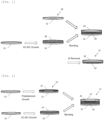
- FIG. 1 a method for manufacturing a 3C-SiC laminate substrate according to the first embodiment of the present invention is described, referring to FIG. 1 .
- FIG. 1 is a view illustrating an example of the manufacturing flow of the laminate substrate, and a view illustrating the manufacturing flow of the laminate substrate composed of a single crystal silicon substrate and a 3C-SiC.
- the inventive method for manufacturing a 3C-SiC laminate substrate includes the steps of epitaxially growing a 3C-SiC single crystal film 10 on a first single crystal silicon substrate 11, bonding a support substrate 20 on an upper surface of the 3C-SiC single crystal film, and removing the first single crystal silicon substrate 11 to manufacture a 3C-SiC laminate substrate 31.
- the first single crystal silicon substrate 11 (low-resistance substrate: resistivity is preferably 0.001 ⁇ cm or higher and less than 0.1 ⁇ cm, for example, 0.005 ⁇ cm) is placed in a reduced pressure (RP)-CVD apparatus and a native oxide film on a surface is removed by hydrogen baking (H 2 anneal).
- H 2 anneal When an oxide film remains, nucleation of SiC cannot be performed on the first single crystal silicon substrate 11.
- the H 2 anneal at this time preferably has a condition of a temperature of 1000°C or higher and 1200°C or lower. When the temperature is lower than 1000°C, a prolonged processing time is required to prevent the residual native oxide film. Conversely, the temperature exceeding 1200°C raises concerns about slip generation.
- a pressure and time for the H 2 annealing at this time are not particularly limited as long as the native oxide film is removed.
- the RP-CVD apparatus it is possible to handle a substrate having a large diameter.
- the substrate having a diameter of 200mm or larger, 450 mm or smaller is used as the first single crystal silicon substrate 11.
- the first single crystal silicon substrate 11 a substrate having a thickness of approximately 770 ⁇ m is used.
- a carbonization gas such as a propane gas or a gas containing carbon and silicon such as trimethylsilane gas is introduced as a raw material gas.
- the temperature thereof is then gradually raised from a temperature in a range of 300°C or higher and 950°C or lower to a temperature in a range of 1000°C or higher and lower than 1200°C.
- a growth rate is in a range of 0.5 to 5°C/min, and approximately 1°C/min is preferable.
- the growth may either be stopped or continued until reaching a predetermined film thickness. Alternatively, when reaching the predetermined film thickness during the temperature rise, the growth may be stopped at that point.
- a gradual increase in a film-forming rate is enabled by continuously changing a growth mode. This forms the SiC single crystal film 10.
- the support substrate 20 having the same diameter is provided, and bonding therebetween is performed.
- a second single crystal silicon substrate 12 (high-resistance substrate: a resistivity thereof is preferably 500 ⁇ cm or higher and 10000 ⁇ cm or lower, for example, larger than 1000 ⁇ cm) is bonded as the support substrate 20, at this time, a surface of the 3C-SiC substrate 10 described above may be bonded to the support substrate 20 as is, or the bonding may be performed after activating the surfaces of the respective substrates by using gases such as O 2 , N 2 , or O 3 activated by plasma.
- the bonding strength by heat treatment is further enhanced by processing at 300 to 600°C for a short time after bonding but not mandatory.
- the first single crystal silicon substrate 11 having low resistance is removed.
- Silicon having a thickness of approximately 770 ⁇ m may be completely etched using nitrohydrofluoric acid, and grinding and polishing may be combined.
- the low-resistance substrate side has a faster etching rate compared to the high-resistance substrate, only the first single crystal silicon substrate 11 is removed by etching, and the second single crystal silicon substrate 12, being the support substrate 20, is not etched away completely.
- the 3C-SiC laminate substrate 31, in which the 3C-SiC single crystal film 10 is laminated on the single crystal silicon substrate 12 and the 3C-SiC single crystal film has a diameter of 200 mm or larger, can be obtained.
- FIG. 2 is a view illustrating another example of the manufacturing flow of a laminate substrate, and a view illustrating the manufacturing flow of the laminate substrate composed of a single crystal silicon substrate, a diamond, a 3C-SiC, and a single crystal silicon substrate.
- the second embodiment has the same configuration as the first embodiment except that, a support substrate 20 in which a diamond 15 is grown on a third single crystal silicon substrate 13 is used instead of a second single crystal silicon substrate 12 as a support substrate 20, and the single crystal silicon substrate is not removed after bonding.
- the support substrate 20 having the same diameter as a first single crystal silicon substrate 11 is provided.
- the support substrate 20 is a substrate in which the diamond 15 is grown on the third single crystal silicon substrate 13.
- this substrate is formed by growing the diamond 15 on the third single crystal silicon substrate 13 by a hot-filament method.
- Bonding is performed using this support substrate 20.
- N 2 plasma is used when bonding.
- O 2 or O 3 is used, the diamond is vaporized by oxidation.
- the single crystal silicon substrate 13, the diamond 15, a 3C-SiC single crystal film 10, and the single crystal silicon substrate 11 are laminated in this order, and then a 3C-SiC laminate substrate 31 is obtained.
- the 3C-SiC single crystal film 10 preferably has a diameter of 200 mm or larger and 450 mm or smaller. Since a configuration in which the 3C-SiC single crystal film 10 on the diamond 15 with high thermal conductivity is laminated, it can be applied to a power device or a high-frequency device.
- the first single crystal silicon substrate may be removed to make a three-layer laminate substrate, depending on the purpose.
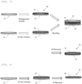
- FIG. 3 is a view illustrating a further example of the manufacturing flow of a laminate substrate, and a view illustrating the manufacturing flow of the laminate substrate composed of a diamond and a 3C-SiC.
- the third embodiment has the same configuration as the second embodiment except that a first and a third single crystal silicon substrate are removed after bonding.
- 3C-SiC laminate substrate can be obtained, in which a single crystal silicon substrate, a diamond, a 3C-SiC single crystal film, and a single crystal silicon substrate are laminated in this order, by bonding in the same configuration as in the second embodiment.
- Both single crystal silicon substrates are removed after bonding. At that time, only low-resistance silicon can be etched when nitrohydrofluoric acid is used. Consequently, by making not only a first single crystal silicon substrate 11 but also a third single crystal silicon substrate 13 into the low-resistance substrates (preferably, a resistivity is 0.001 ⁇ cm or higher and less than 0.1 ⁇ cm, for example, 0.005 ⁇ cm), then after bonding, not only the first single crystal silicon substrate 11 but also the third single crystal silicon substrate 13 can be removed.
- the 3C-SiC single crystal film 10 is laminated on the diamond 15, and then a 3C-SiC laminate substrate 31 is obtained.
- the 3C-SiC single crystal film 10 preferably has a diameter of 200 mm or larger and 450 mm or smaller. Since a configuration is composed of the 3C-SiC single crystal film 10 laminated on the diamond 15 with high thermal conductivity, it can be applied to a power device or a high-frequency device.
- FIG. 4 is a view illustrating an example of a flow diagram for manufacturing a freestanding substrate.
- a first single crystal silicon substrate 11 (low-resistance substrate: resistivity is preferably 0.001 ⁇ cm or higher and less than 0.1 ⁇ cm, for example, 0.005 ⁇ cm) is placed in a reduced pressure (RP)-CVD apparatus and a native oxide film on a surface is removed by hydrogen baking (H 2 anneal).
- H 2 anneal When an oxide film remains, nucleation of SiC cannot be performed on the first single crystal silicon substrate 11.
- the H 2 anneal at this time preferably has a condition of a temperature of 1000°C or higher and 1200°C or lower. When the temperature is lower than 1000°C, a prolonged processing time is required to prevent the residual native oxide film. Conversely, the temperature exceeding 1200°C raises concerns about slip generation.
- a pressure and time for the H 2 annealing at this time are not particularly limited as long as the native oxide film is removed.
- the RP-CVD apparatus it is possible to handle a substrate having a large diameter.
- a substrate having a diameter of 200mm or larger and 450 mm or smaller is used as the first single crystal silicon substrate 11.
- the first single crystal silicon substrate 11 a substrate having a thickness of approximately 770 ⁇ m is used.
- the temperature thereof is then gradually raised from a temperature in a range of 300°C or higher and 950°C or lower to a temperature in a range of 1000°C or higher and lower than 1200°C.
- a growth rate is in a range of 0.5 to 5°C/min, and approximately 1°C/min is preferable. At this point, after the temperature is raised to a predetermined temperature, the growth may either be stopped or continued until reaching a predetermined film thickness.
- the growth when reaching the predetermined film thickness during the temperature rise, the growth may be stopped at that point.
- a gradual increase in a film-forming rate is enabled by continuously changing a growth mode. This forms a 3C-SiC single crystal film 10.
- the first single crystal silicon substrate 11 (low-resistance substrate: resistivity is preferably 0.001 ⁇ cm or higher and less than 0.1 ⁇ cm, for example, 0.005 ⁇ cm) is removed. Silicon having a thickness of approximately 770 ⁇ m may be completely etched using nitrohydrofluoric acid, and grinding and polishing may be combined.
- a freestanding 3C-SiC substrate 32 being a substrate composed of the 3C-SiC single crystal film 10 where the 3C-SiC single crystal film has a diameter of 200 mm or larger, can be obtained.
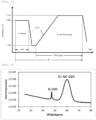
- FIG. 5 is a view illustrating an example of a growth sequence of 3C-SiC.
- 3C-SiC growths in Examples 1 and 2 were performed according to the growth sequence of 3C-SiC shown in FIG. 5 .
- a boron-doped single crystal silicon (111) substrate having low resistance (resistivity: 0.005 ⁇ cm, hereinafter also referred to as "wafer") and a diameter of 300 mm was provided.
- the wafer was placed on a susceptor in a reaction furnace of an RP-CVD apparatus and then H 2 anneal was performed at 1080°C for 1 minute.
- trimethylsilane gas was introduced while raising the temperature to 1130°C at a temperature rise rate of 1°C/sec, and nucleation of SiC and subsequent formation of a 3C-SiC single crystal film were performed.
- a growth pressure at this time was set to 100 Torr (13332.2 Pa) uniformly. After reaching 1130°C, the temperature was held for 10 minutes, and the growth of the 3C-SiC single crystal film was performed (film thickness: 200 nm).
- a boron-doped single crystal silicon (111) substrate having high resistance (resistivity: 1000 ⁇ cm) and a diameter of 300 mm was provided. Both bonding surfaces of the silicon and the 3C-SiC were irradiated with N 2 plasma (250 Torr (33330.6 Pa), N 2 : 300 sccm, RF power 100 W, 10 minutes), then bonded to each other.
- the 3C-SiC film was then confirmed by XRD in an In-plane arrangement.
- FIG. 6 is a view illustrating a result of an In-plane XRD analysis of a 3C-SiC (111) laminate substrate manufactured in Example 1.
- a boron-doped single crystal silicon (111) substrate having low resistance (resistivity: 0.005 ⁇ cm, hereinafter also referred to as "wafer") having a diameter of 300 mm was provided.
- the wafer was placed on a susceptor in a reaction furnace of an RP-CVD apparatus and then H 2 anneal was performed at 1080°C for 1 minute.
- trimethylsilane gas was introduced while raising the temperature to 1130°C at a temperature rise rate of 1°C/sec, and a nucleation step of SiC and subsequent formation of a 3C-SiC single crystal film were performed.
- a growth pressure at this time was set to 100 Torr (13332.2 Pa) uniformly. After reaching 1130°C, the temperature was held for 10 minutes, and the growth of the 3C-SiC single crystal film was performed (film thickness: 200 nm).
- a boron-doped single crystal silicon (111) substrate having low resistance (resistivity: 0.005 ⁇ cm) and a diameter of 300 mm was provided. Polydiamond was then grown thereon for 100 ⁇ m by a hot-filament CVD apparatus (5 Torr (666.612 Pa), filament temperature: 2250°C, CH 4 : 1%).
- both bonding surfaces of the silicon and the 3C-SiC were irradiated with N 2 plasma (250 Torr (33330.6 Pa), N 2 : 300 sccm, RF power 100 W, 10 minutes), then bonded to each other.
- the 3C-SiC film was then confirmed by XRD in an In-plane arrangement.
- FIG. 7 is a view illustrating a result of an In-plane XRD analysis of a 3C-SiC (111) laminate substrate manufactured in Example 2.
- the 3C-SiC laminate substrate having a large diameter and few defects was successfully manufactured in an easy and reliable manner.
- the present description includes the following embodiments.
Landscapes
- Chemical & Material Sciences (AREA)
- Engineering & Computer Science (AREA)
- Crystallography & Structural Chemistry (AREA)
- Materials Engineering (AREA)
- Metallurgy (AREA)
- Organic Chemistry (AREA)
- Chemical Kinetics & Catalysis (AREA)
- General Chemical & Material Sciences (AREA)
- Inorganic Chemistry (AREA)
- Crystals, And After-Treatments Of Crystals (AREA)
- Recrystallisation Techniques (AREA)
Applications Claiming Priority (2)
| Application Number | Priority Date | Filing Date | Title |
|---|---|---|---|
| JP2022124317 | 2022-08-03 | ||
| PCT/JP2023/022801 WO2024029217A1 (fr) | 2022-08-03 | 2023-06-20 | Procédé de fabrication de substrat stratifié à base de 3c-sic, substrat stratifié à base de 3c-sic et substrat indépendant à base de 3c-sic |
Publications (1)
| Publication Number | Publication Date |
|---|---|
| EP4567165A1 true EP4567165A1 (fr) | 2025-06-11 |
Family
ID=89848812
Family Applications (1)
| Application Number | Title | Priority Date | Filing Date |
|---|---|---|---|
| EP23849777.0A Pending EP4567165A1 (fr) | 2022-08-03 | 2023-06-20 | Procédé de fabrication de substrat stratifié à base de 3c-sic, substrat stratifié à base de 3c-sic et substrat indépendant à base de 3c-sic |
Country Status (6)
| Country | Link |
|---|---|
| EP (1) | EP4567165A1 (fr) |
| JP (1) | JPWO2024029217A1 (fr) |
| KR (1) | KR20250044274A (fr) |
| CN (1) | CN119677900A (fr) |
| TW (1) | TW202408802A (fr) |
| WO (1) | WO2024029217A1 (fr) |
Family Cites Families (10)
| Publication number | Priority date | Publication date | Assignee | Title |
|---|---|---|---|---|
| JPS53146300A (en) * | 1977-05-25 | 1978-12-20 | Sharp Corp | Production of silicon carbide substrate |
| JPH10324599A (ja) * | 1997-05-20 | 1998-12-08 | Denso Corp | 炭化珪素単結晶の製造方法 |
| JPH11268995A (ja) * | 1998-03-20 | 1999-10-05 | Denso Corp | 炭化珪素単結晶の製造方法 |
| CN100433257C (zh) * | 2004-01-15 | 2008-11-12 | 野田优 | 制造单晶薄膜的方法 |
| JP2006253617A (ja) | 2005-02-14 | 2006-09-21 | Toshiba Ceramics Co Ltd | SiC半導体およびその製造方法 |
| JP2008184361A (ja) | 2007-01-30 | 2008-08-14 | Covalent Materials Corp | 3C−SiC単結晶膜の形成方法 |
| WO2017013445A1 (fr) | 2015-07-23 | 2017-01-26 | The University Of Warwick | Croissance épitaxiale de 3c-sic sur du silicium monocristallin |
| JP6450282B2 (ja) | 2015-08-19 | 2019-01-09 | エア・ウォーター株式会社 | 化合物半導体基板および化合物半導体基板の製造方法 |
| JP7259615B2 (ja) | 2019-07-24 | 2023-04-18 | 株式会社Sumco | ヘテロエピタキシャルウェーハの製造方法 |
| EP4131343A4 (fr) * | 2020-04-03 | 2023-05-31 | Mitsubishi Electric Corporation | Procédé de polissage et procédé de production de substrat semi-conducteur |
-
2023
- 2023-06-20 WO PCT/JP2023/022801 patent/WO2024029217A1/fr not_active Ceased
- 2023-06-20 KR KR1020257003058A patent/KR20250044274A/ko active Pending
- 2023-06-20 CN CN202380055877.8A patent/CN119677900A/zh active Pending
- 2023-06-20 JP JP2024538853A patent/JPWO2024029217A1/ja active Pending
- 2023-06-20 EP EP23849777.0A patent/EP4567165A1/fr active Pending
- 2023-06-28 TW TW112124030A patent/TW202408802A/zh unknown
Also Published As
| Publication number | Publication date |
|---|---|
| TW202408802A (zh) | 2024-03-01 |
| WO2024029217A1 (fr) | 2024-02-08 |
| JPWO2024029217A1 (fr) | 2024-02-08 |
| KR20250044274A (ko) | 2025-03-31 |
| CN119677900A (zh) | 2025-03-21 |
Similar Documents
| Publication | Publication Date | Title |
|---|---|---|
| TWI313892B (en) | Low 1c screw dislocation 3 inch silicon carbide wafer | |
| JP5693946B2 (ja) | 単結晶3C−SiC基板の製造方法 | |
| EP3351660B1 (fr) | Procédé de fabrication d'un substrat composite à base de sic | |
| JP6631517B2 (ja) | ダイヤモンド基板、及び、ダイヤモンド複合基板 | |
| EP3352197B1 (fr) | PROCÉDÉ DE FABRICATION D'UN SUBSTRAT COMPOSITE DE SiC | |
| CN121519022A (zh) | 金刚石衬底及其制造方法 | |
| KR20120001606A (ko) | 단결정 다이아몬드 성장용 기재 및 단결정 다이아몬드 기판의 제조 방법 | |
| CN102465343A (zh) | 制造GaN基膜的方法 | |
| JP4946264B2 (ja) | 炭化珪素半導体エピタキシャル基板の製造方法 | |
| CN104867818B (zh) | 一种减少碳化硅外延材料缺陷的方法 | |
| CN102465342B (zh) | 制造GaN基膜的方法 | |
| JP7259906B2 (ja) | ヘテロエピタキシャルウェーハの製造方法 | |
| JP2010034330A (ja) | エピタキシャルウェーハおよびその製造方法 | |
| JP6927429B2 (ja) | SiCエピタキシャル基板の製造方法 | |
| EP4567165A1 (fr) | Procédé de fabrication de substrat stratifié à base de 3c-sic, substrat stratifié à base de 3c-sic et substrat indépendant à base de 3c-sic | |
| EP4653588A1 (fr) | Procédé de fabrication d'un substrat épitaxial de 3c-sic monocristallin, procédé de fabrication d'un substrat autoporteur de 3c-sic, et substrat épitaxial de 3c-sic monocristallin | |
| JP5135545B2 (ja) | 炭化珪素単結晶インゴット育成用種結晶及びその製造方法 | |
| JP7218832B1 (ja) | ヘテロエピタキシャルウェーハの製造方法 | |
| CN102017080A (zh) | 制造Si(1-v-w-x)CwAlxNv衬底的方法、制造外延晶片的方法、Si(1-v-w-x)CwAlxNv衬底以及外延晶片 | |
| CN102016135A (zh) | 制造Si(1-v-w-x)CwAlxNv衬底的方法、制造外延晶片的方法、Si(1-v-w-x)CwAlxNv衬底以及外延晶片 | |
| TW202332044A (zh) | 用於製作包含多晶碳化矽底材及單晶碳化矽主動層之半導體結構之方法 | |
| TW202605916A (zh) | 經由遠端磊晶的SiC層轉移 | |
| KR20240088776A (ko) | 헤테로에피택셜막의 제작방법 | |
| CN118556140A (zh) | 单晶金刚石膜的形成方法 | |
| JP2009032707A (ja) | Si基板表面の炭化による結晶性SiCの形成方法及び結晶性SiC基板 |
Legal Events
| Date | Code | Title | Description |
|---|---|---|---|
| STAA | Information on the status of an ep patent application or granted ep patent |
Free format text: STATUS: THE INTERNATIONAL PUBLICATION HAS BEEN MADE |
|
| PUAI | Public reference made under article 153(3) epc to a published international application that has entered the european phase |
Free format text: ORIGINAL CODE: 0009012 |
|
| STAA | Information on the status of an ep patent application or granted ep patent |
Free format text: STATUS: REQUEST FOR EXAMINATION WAS MADE |
|
| 17P | Request for examination filed |
Effective date: 20250121 |
|
| AK | Designated contracting states |
Kind code of ref document: A1 Designated state(s): AL AT BE BG CH CY CZ DE DK EE ES FI FR GB GR HR HU IE IS IT LI LT LU LV MC ME MK MT NL NO PL PT RO RS SE SI SK SM TR |
|
| DAV | Request for validation of the european patent (deleted) | ||
| DAX | Request for extension of the european patent (deleted) |