EP4572595A1 - Integrierte schaltung mit nichtflüchtigem speicher und herstellungsverfahren dafür - Google Patents
Integrierte schaltung mit nichtflüchtigem speicher und herstellungsverfahren dafür Download PDFInfo
- Publication number
- EP4572595A1 EP4572595A1 EP24307084.4A EP24307084A EP4572595A1 EP 4572595 A1 EP4572595 A1 EP 4572595A1 EP 24307084 A EP24307084 A EP 24307084A EP 4572595 A1 EP4572595 A1 EP 4572595A1
- Authority
- EP
- European Patent Office
- Prior art keywords
- layer
- substrate
- contact
- heating element
- diffusion barrier
- Prior art date
- Legal status (The legal status is an assumption and is not a legal conclusion. Google has not performed a legal analysis and makes no representation as to the accuracy of the status listed.)
- Pending
Links
Images






Classifications
-
- H—ELECTRICITY
- H10—SEMICONDUCTOR DEVICES; ELECTRIC SOLID-STATE DEVICES NOT OTHERWISE PROVIDED FOR
- H10B—ELECTRONIC MEMORY DEVICES
- H10B63/00—Resistance change memory devices, e.g. resistive RAM [ReRAM] devices
- H10B63/80—Arrangements comprising multiple bistable or multi-stable switching components of the same type on a plane parallel to the substrate, e.g. cross-point arrays
- H10B63/82—Arrangements comprising multiple bistable or multi-stable switching components of the same type on a plane parallel to the substrate, e.g. cross-point arrays the switching components having a common active material layer
-
- H—ELECTRICITY
- H10—SEMICONDUCTOR DEVICES; ELECTRIC SOLID-STATE DEVICES NOT OTHERWISE PROVIDED FOR
- H10N—ELECTRIC SOLID-STATE DEVICES NOT OTHERWISE PROVIDED FOR
- H10N70/00—Solid-state devices having no potential barriers, and specially adapted for rectifying, amplifying, oscillating or switching
- H10N70/801—Constructional details of multistable switching devices
- H10N70/841—Electrodes
- H10N70/8413—Electrodes adapted for resistive heating
-
- H—ELECTRICITY
- H10—SEMICONDUCTOR DEVICES; ELECTRIC SOLID-STATE DEVICES NOT OTHERWISE PROVIDED FOR
- H10B—ELECTRONIC MEMORY DEVICES
- H10B63/00—Resistance change memory devices, e.g. resistive RAM [ReRAM] devices
- H10B63/10—Phase change RAM [PCRAM, PRAM] devices
-
- H—ELECTRICITY
- H10—SEMICONDUCTOR DEVICES; ELECTRIC SOLID-STATE DEVICES NOT OTHERWISE PROVIDED FOR
- H10B—ELECTRONIC MEMORY DEVICES
- H10B63/00—Resistance change memory devices, e.g. resistive RAM [ReRAM] devices
- H10B63/20—Resistance change memory devices, e.g. resistive RAM [ReRAM] devices comprising selection components having two electrodes, e.g. diodes
- H10B63/24—Resistance change memory devices, e.g. resistive RAM [ReRAM] devices comprising selection components having two electrodes, e.g. diodes of the Ovonic threshold switching type
-
- H—ELECTRICITY
- H10—SEMICONDUCTOR DEVICES; ELECTRIC SOLID-STATE DEVICES NOT OTHERWISE PROVIDED FOR
- H10N—ELECTRIC SOLID-STATE DEVICES NOT OTHERWISE PROVIDED FOR
- H10N70/00—Solid-state devices having no potential barriers, and specially adapted for rectifying, amplifying, oscillating or switching
- H10N70/011—Manufacture or treatment of multistable switching devices
-
- H—ELECTRICITY
- H10—SEMICONDUCTOR DEVICES; ELECTRIC SOLID-STATE DEVICES NOT OTHERWISE PROVIDED FOR
- H10N—ELECTRIC SOLID-STATE DEVICES NOT OTHERWISE PROVIDED FOR
- H10N70/00—Solid-state devices having no potential barriers, and specially adapted for rectifying, amplifying, oscillating or switching
- H10N70/011—Manufacture or treatment of multistable switching devices
- H10N70/021—Formation of switching materials, e.g. deposition of layers
-
- H—ELECTRICITY
- H10—SEMICONDUCTOR DEVICES; ELECTRIC SOLID-STATE DEVICES NOT OTHERWISE PROVIDED FOR
- H10N—ELECTRIC SOLID-STATE DEVICES NOT OTHERWISE PROVIDED FOR
- H10N70/00—Solid-state devices having no potential barriers, and specially adapted for rectifying, amplifying, oscillating or switching
- H10N70/011—Manufacture or treatment of multistable switching devices
- H10N70/061—Shaping switching materials
- H10N70/063—Shaping switching materials by etching of pre-deposited switching material layers, e.g. lithography
-
- H—ELECTRICITY
- H10—SEMICONDUCTOR DEVICES; ELECTRIC SOLID-STATE DEVICES NOT OTHERWISE PROVIDED FOR
- H10N—ELECTRIC SOLID-STATE DEVICES NOT OTHERWISE PROVIDED FOR
- H10N70/00—Solid-state devices having no potential barriers, and specially adapted for rectifying, amplifying, oscillating or switching
- H10N70/20—Multistable switching devices, e.g. memristors
- H10N70/231—Multistable switching devices, e.g. memristors based on solid-state phase change, e.g. between amorphous and crystalline phases, Ovshinsky effect
-
- H—ELECTRICITY
- H10—SEMICONDUCTOR DEVICES; ELECTRIC SOLID-STATE DEVICES NOT OTHERWISE PROVIDED FOR
- H10N—ELECTRIC SOLID-STATE DEVICES NOT OTHERWISE PROVIDED FOR
- H10N70/00—Solid-state devices having no potential barriers, and specially adapted for rectifying, amplifying, oscillating or switching
- H10N70/801—Constructional details of multistable switching devices
- H10N70/821—Device geometry
- H10N70/826—Device geometry adapted for essentially vertical current flow, e.g. sandwich or pillar type devices
-
- H—ELECTRICITY
- H10—SEMICONDUCTOR DEVICES; ELECTRIC SOLID-STATE DEVICES NOT OTHERWISE PROVIDED FOR
- H10N—ELECTRIC SOLID-STATE DEVICES NOT OTHERWISE PROVIDED FOR
- H10N70/00—Solid-state devices having no potential barriers, and specially adapted for rectifying, amplifying, oscillating or switching
- H10N70/801—Constructional details of multistable switching devices
- H10N70/881—Switching materials
- H10N70/882—Compounds of sulfur, selenium or tellurium, e.g. chalcogenides
-
- H—ELECTRICITY
- H10—SEMICONDUCTOR DEVICES; ELECTRIC SOLID-STATE DEVICES NOT OTHERWISE PROVIDED FOR
- H10N—ELECTRIC SOLID-STATE DEVICES NOT OTHERWISE PROVIDED FOR
- H10N70/00—Solid-state devices having no potential barriers, and specially adapted for rectifying, amplifying, oscillating or switching
- H10N70/801—Constructional details of multistable switching devices
- H10N70/881—Switching materials
- H10N70/882—Compounds of sulfur, selenium or tellurium, e.g. chalcogenides
- H10N70/8828—Tellurides, e.g. GeSbTe
-
- H—ELECTRICITY
- H10—SEMICONDUCTOR DEVICES; ELECTRIC SOLID-STATE DEVICES NOT OTHERWISE PROVIDED FOR
- H10N—ELECTRIC SOLID-STATE DEVICES NOT OTHERWISE PROVIDED FOR
- H10N70/00—Solid-state devices having no potential barriers, and specially adapted for rectifying, amplifying, oscillating or switching
- H10N70/801—Constructional details of multistable switching devices
- H10N70/881—Switching materials
- H10N70/883—Oxides or nitrides
Definitions
- the technical field of the invention relates to integrated circuits comprising non-volatile memories and more particularly implementing a phase change material, known as PCM memory for "Phase Change Material" in English.
- PCM memory for "Phase Change Material” in English.
- the technical field relates, for example, to integrated circuits that can be implemented in the automotive field.
- a non-volatile memory using a phase change material can be characterized by its resistance, which can take at least two distinct values. Each resistance value corresponds to a distinct state that the memory can take, thus allowing binary information to be stored.
- a high resistance value corresponds to a state called “RESET”, generally associated with a low state or "0".
- a low resistance value corresponds to a state called “SET”, generally associated with a high state or "1".
- Programming the memory from one state to another, or from one resistance value to another can be carried out following the so-called “RESET” programming or “SET” programming steps.
- the "RESET” programming is based on the melting of all or part of the volume of the phase change material (for example a chalcogenide) which is reached by an electrical pulse with a sufficiently high current.
- the current is sized to allow reaching a melting temperature of the PCM material by Joule effect.
- a sudden cooling, obtained by a rapid reduction of the applied current, allows to leave the melted part of the PCM material in an amorphous state.
- This amorphous arrangement has a high resistance, corresponding to the RESET state.
- SET programming is based on obtaining a crystalline state of the PCM material. This operation consists of applying an electrical pulse which produces, by Joule effect, a partial or total melting of the PCM material. A gradual reduction of the applied current allows the PCM material to be recrystallized. This crystalline state, with lower resistance, corresponds to the SET state.
- Information retention can be characterized by the duration of the RESET state as a function of time and temperature.
- Information retention specifications can be strict for embedded applications. For example, a so-called "JEDEC" standard, applied to automobiles, requires a RESET state stability of two years at a temperature of 150°C.
- PCM Phase Change Memory
- the document [ « Optimization Metrics for Phase Change Memory (PCM) Cell Architectures”, M. Boniardi et al., IEDM14 IEEE 2014 ] discloses a non-volatile memory comprising a layer of PCM material and a heater connected in series.
- the heater is notably of the "WALL" type, i.e. having a fin shape, extending perpendicular to the plane of the layers.
- WALL Wideband
- the temperatures accessible with this type of heater make it possible to improve the programming efficiency of the PCM layer.
- the PCM layer/heater assembly is connected in series between two metal electrodes, in this case tungsten. The application of an electrical potential to the terminals of the tungsten electrodes causes the circulation of an electric current which, by Joule effect in the resistive heater, causes localized heating of the PCM layer.
- non-volatile memories can be separated from the "start-of-line functional block" of the integrated circuit, also called “Primary Manufacturing Level” or “FEOL” for "Front-end of Line” in English, in which logic circuits, for example of the "CMOS” type (for “Complementary Metal Oxide Semiconductor”) are integrated.
- CMOS complementary Metal Oxide Semiconductor
- the electrical connection between the different levels of the integrated circuit i.e. between the logic circuits of the FEOL and the memories of the different levels of the BEOL, is achieved by means of routing levels comprising copper vias, crossing the different levels of the circuit.
- the integration of PCM layers in the vicinity of copper vias is problematic. Indeed, copper is an element that can degrade PCM layers.
- copper diffusion can be assisted by temperature.
- the manufacturing of memories or the circulation of current in heating elements assists copper diffusion and can cause degradation of PCM layers. There is therefore a need to integrate a PCM layer at the BEOL level while avoiding the pitfalls related to copper diffusion.
- the document [“ 18 nm FDSOI Technology Platform embedding PCM & innovative Continuous-Active Construct Enhancing Performance for Leading-Edge MCU Application”, D. Min et al., IEDM21 IEEE 2021 ] also discloses a non-volatile memory integrated in an integrated circuit, comprising a PCM layer shared between several WALL-type heating elements. Each heating element is, here, connected in series between a tungsten contact called a buffer layer or “plug” in English and the PCM layer.
- the formation of the buffer layer involves several manufacturing steps.
- its significant thickness poses integration problems in the BEOL where the thickness between the different levels, within an integrated circuit, can be constrained.
- the invention provides a means of blocking the diffusion of copper between a routing level and a memory which may be impacted. by the diffusion of copper, having a low thickness and whose manufacture is simple.
- a flat surface means a surface extending in a plane (e.g. a horizontal plane).
- Via means a conductive track extending into the substrate, for example in a direction perpendicular to the surface of the substrate.
- Line means a conductive track extending into the substrate, for example in a direction parallel to the surface of the substrate.
- active layer is meant a layer whose resistance can vary, reversibly or irreversibly, following the flow of a current or the application of a heat treatment.
- the first active layer can change of resistance between at least two distinct values, in a bistable manner, allowing information to be stored.
- Non-volatile memory is preferably understood to mean phase change memory.
- parallel and perpendicular we mean respectively parallel to within 20o, or even parallel to within 10o, and perpendicular to within 20o, or even perpendicular to within 10o.
- in contact is meant that there is no intermediate element between the elements in contact. Typically, there is no intermediate layer between two elements in contact, in particular between the heating element and the first active layer, nor between the volatile memory and the diffusion barrier.
- Each barrier layer prevents copper from diffusing into the memory and/or the heating element during IC fabrication or use. This layer replaces the use of a tungsten buffer layer.
- the diffusion barrier allows the non-volatile memory to be manufactured at the BEOL of the integrated circuit and thus to be kept away from the logic circuits of the FEOL of the integrated circuit. This arrangement prevents non-volatile memories from being able to disrupt the operation of the logic circuits of the FEOL.
- Ta, Ti, Co-based materials are sufficiently effective to block copper diffusion while allowing a diffusion barrier to be produced in the form of a thin layer.
- the diffusion barriers according to the invention make it possible to significantly reduce the total height of each non-volatile memory.
- Ta, Ti or Co-based barriers offer easier integration of non-volatile memories. They offer the possibility of using the resulting integrated circuit at a higher frequency. Indeed, the height between the different levels of the BEOL can be constrained by the height of the non-volatile memories. Reducing the height of the memories makes it possible to reduce the thickness between the different levels of the BEOL. The length of the copper vias connecting these levels can then also be reduced. Thus, the resistance of each via and the coupling capacitive between the vias decreases, allowing the circuit to be used at higher frequencies.
- Diffusion barriers can be implemented at different levels of the integrated circuit, for example closest to the FEOL.
- each heating element comprises a portion, called a "fin", extending perpendicular to the surface of the substrate and comprising a first end, in contact with the first active layer of said non-volatile memory, and a second end, in contact with said at least one diffusion barrier.
- each diffusion barrier extends against the entire contact surface of a via or of said at least one copper line.
- the blocking of diffusion is improved.
- each diffusion barrier extends beyond said contact surface by also extending onto the flat surface of the substrate.
- each heating element comprises one of: TiN, TiC, TiSiN, TiSiCN, TiWN, TaN and TaCN.
- the first active layer of each volatile memory comprises a chalcogenide material.
- the first layer is programmable.
- the first active layers of the different non-volatile memories are laterally isolated from each other.
- laterally isolated is meant that the first active layers are without direct contact.
- the same first active layer is continuous and common to at least two non-volatile memories, said same first active layer being in contact with each heating element of said at least two non-volatile memories.
- the first active layers can thus be shared between several non-volatile memories. This makes it possible, for example, to reduce the number of operations for producing the first active layers, in particular the number of etchings.
- the integrated circuit comprises a selection element associated with said at least one non-volatile memory. It allows addressing of each memory.
- This configuration makes it possible to have a selector in the BEOL, with each memory.
- This arrangement makes it possible to dispense with the use of a logic component, for example a CMOS transistor of the FEOL as a selector. This arrangement thus makes it possible to dispense with the technology implemented in the FEOL and makes each memory portable.
- the selection element is an ovonic threshold switch called “OTS”, preferably comprising an alloy based on Ge, Sb, Se, As, Si, Te, S or Al, which can be doped, such as alloys of GeSbSe, GeSe, AsSeSiGe, AsSe, SbSe, SiSe, AsTe, SiGeSe or AlTe.
- OTS ovonic threshold switch
- the integrated circuit is devoid of tungsten via or metal via in contact with said at least one copper via or said at least one copper line and the heating element of said at least one non-volatile memory.
- the at least one diffusion barrier is a planar bilayer, the planar bilayer comprising TaN in contact with the via or the line, and comprising Ta in contact with the heating element.
- a buffer for example, made of tungsten
- five additional steps including a chemical-physical polishing step.
- the formation of diffusion barriers requires at most two steps (e.g., deposition of a layer and its delimitation). The number and complexity of the steps are reduced.
- each diffusion barrier comprises the step of growing said diffusion barrier by selective deposition of tantalum or titanium or cobalt or their alloys on the contact surface of a copper via or a copper line.
- growth by selective deposition makes it possible to localize the growth of diffusion barriers at the contact surface of the vias or copper lines.
- the etching of the barrier material layer is carried out so as to form diffusion barriers separated from each other.
- the etching of the barrier material layer through said at least one mask is carried out so that each diffusion barrier extends in the form of a layer against at least part of the contact surface of said at least one via or of said at least one line.
- Conformal deposition of the resistive layer on the first dielectric layer forms a resistive layer having portions parallel to the substrate and a portion perpendicular to the substrate.
- the parallel portions of the resistive layer are removed by etching.
- the perpendicular portion of the resistive layer is retained because it has a thickness, measured perpendicular to the substrate, that is much greater than the parallel portions. This perpendicular portion thus forms the fin.
- the first etching mask and the fin extending against the flank of the first dielectric layer then form a first etching mask protecting a portion of the barrier material layer from etching.
- the fin is at least in contact with the portion of the barrier material layer that it protects from etching.
- Etching through the second mask allows each diffusion barrier and each heating element to be delimited in the extension of a via or a line.
- Each non-volatile memory thus comprises a first active layer aligned with a heating element.
- the coupling between the first active layer and the heating element is therefore controlled and identical for different non-volatile memories.
- This alignment also makes it possible to eliminate spatial drift due to several etching steps carried out at different levels.
- the non-volatile memory is also aligned with a diffusion barrier, ensuring effective protection of the first active layer from the copper.
- the second etching mask is configured so that the first active layers of the two non-volatile memories form a single layer.
- the first two active layers form, for example, an island or a line.
- the method also comprises the step of forming a selection element associated with each non-volatile memory, in contact with the upper electrode of each non-volatile memory.
- the at least one diffusion barrier is etched a first time in a first direction during the formation of the heating element, and a second time in a second direction, different from the first direction, during the formation, for example by etching, of the upper electrode.
- FIG. 1A And 1B present an integrated circuit 1 according to a first embodiment of the invention.
- the Figure 1B corresponds to an enlargement of the Figure 1A materialized by a dotted rectangle.
- Circuit 1 comprises two functional blocks 2, 3, also called functional levels, which are FEOL 2 (also simply called “front-end” or “FEND”) and BEOL 3 (also simply called “back-end” in English). This type of integrated circuit arrangement or architecture is known to those skilled in the art.
- the integrated circuit 1 comprises at least one non-volatile memory 5, 5'. In the embodiment of the Figures 1A And 1B , it comprises two groups of two non-volatile memories 5, 5'. The memories 5, 5' are arranged in the back-end 3 of the circuit 1.
- the memories 5, 5' are electrically connected to the front-end 2 of the circuit 1 via at least one copper routing level 4, in this case a plurality of levels 4 in this embodiment.
- the memories 5, 5' can be connected to logic components of the front-end 2 playing for example the role of selector of the different memories 5, 5'.
- the memories could also be located directly on front-end 2 (in a level that could be called the "metal level") and directly in contact with the logic components of front-end 2.
- each routing level 4 of the Figures 1A And 1B comprises a substrate 41 and several vias 42.
- the substrate 41 has two planar surfaces 410, 411, opposite one another, called “upper surface” and “lower surface”. They extend in this case in a plane ⁇ X; Y ⁇ .
- Each via 42 of a routing level 4 crosses the substrate 41 from one side to the other, joining the lower surface 411 of the substrate 41 to the upper surface 410 of the substrate 41. More particularly, the vias 42 open from each planar surface 410, 411 by exposing a surface 420 called "contact surface”.
- Each contact surface 420 of the vias 42 is for example parallel and aligned with the planar surfaces 410, 411 of the substrate 41.
- aligned we mean aligned to within 2 nm, preferably less.
- the routing level 4 may comprise lines extending into the substrate 41 and exposing at least one surface equivalent to the contact surface 420 of the vias 42. To simplify the description, only embodiments having vias 42 will be presented.
- the contact surfaces 420 make it possible to make electrical contact with different elements such as a via 42 or a line of an adjacent routing level 4, a heating element 52 of a memory 5 or even a logic component of the front-end 2.
- the 5, 5' memories illustrated in the Figures 1A And 1B comprise a first active layer 51 for storing information.
- An active layer 51 allows, thanks to an internal change, induced by the circulation of a current or a heat treatment, to show a difference in electrical resistance sufficiently significant to be measurable and usable for storing information.
- the first active layer 51 preferably comprises a phase change material for which a heat treatment comprising more or less brief cooling makes it possible to freeze a particular crystalline state.
- the active layer comprises a chalcogenide material.
- the alloy of Ge x Sb y Te z can also comprise other elements of interest such as, for example: N, C, O, Si, Se, Bi, In or even As.
- each memory 5, 5' comprises a first electrode 52, called “lower electrode”, or “heating element” or “heater” or even “conductive finger”, electrically connected to the first active layer 51.
- Each memory 5, 5' also comprises a second electrode 53, called “upper electrode”, also electrically connected to the first active layer 51.
- the first active layer 51 is connected in series between the heating element 52 and the upper electrode 53.
- each heating element 52 is of the “WALL” type.
- the principle of a heating element of this type and the method of connection with an active layer is described in the document [“ Optimization Metrics for Phase Change Memory (PCM) Cell Architectures”, M. Boniardi et al., IEDM14, IEEE 2014 ].
- a heating element 52 of the “WALL” type is remarkable in that it comprises at least a first portion 521, called a “fin”, extending perpendicular to the flat surface 410 of the substrate 41 (in other words in a direction Z).
- the manufacture of a WALL type heating element 52 may frequently involve the presence of a second portion 522, called the “heating element foot” or simply “foot”, consecutive to the fin 521 and extending parallel to the flat surface 410 of the substrate 41 (in other words in the plane ⁇ X; Y ⁇ ).
- the foot 522 is preferably absent, in order to be able to bring the memories 5, 5' closer together and increase the information storage density per unit area.
- Each heating element 52 may be made from a resistive material among: TiN, TiC, TiSiN, TiSiCN, TiWN, TaN and TaCN.
- the first active layer 51 is connected to one of the ends 5211 of the fin 521. This small-sized contact improves the efficiency of the heat treatment that can be applied to the first active layer 51. It allows the programming of this layer 51 to be carried out with reduced energy consumption.
- the foot 522 of the heating element 52 is electrically connected, on the one hand, to a contact surface of a via 42 of a routing level 4 (but not directly in contact with this surface 420) and on the other hand to a second end 5212 of the fin 521.
- Vias 42 of routing levels 4 of the Figures 1A And 1B are made of copper.
- the circuit 1 is remarkable in that it comprises a plurality of copper diffusion barriers 6. Each barrier 6 extends in the form of a thin layer, against the contact surface 420 of a copper via 42. Thus, the diffusion of copper towards the non-volatile memories 5, 5' is blocked.
- one or more, or even all, of the diffusion barriers are planar in shape, or even completely planar in shape. This makes it possible to limit, or even avoid, congestion in the Z direction, while preventing the layer barrier does not bypass the heating element or have to provide spacers.
- the plane in which these diffusion barriers are formed can be a horizontal plane (i.e., in the XY plane) or a vertical plane (i.e., orthogonal to the XY plane).
- each diffusion barrier 6 is made from tantalum or titanium or cobalt or their alloys.
- Said alloys are for example: TaN/Ta, TiN, TiC, TiSiN, TiSiCN, TaN or even TaCN.
- Said alloys can also comprise tungsten, such as TiWN.
- Barriers based on tantalum or titanium or cobalt or their material alloys offer a good blocking capacity for the diffusion of copper atoms even with a limited thickness. It is therefore possible to form diffusion barriers 6 in the form of very thin layers, much thinner than a tungsten pad according to the prior art.
- tungsten pads can have significant roughness, which may require chemical and/or mechanical polishing.
- the diffusion barriers 6, for their part, may have a thickness, measured perpendicular to the upper surface 410 of the substrate, of between 0.5 nm and 20 nm.
- a TaN/Ta barrier 6 may have a thickness of 13 nm.
- each diffusion barrier 6 is a planar bilayer such that the planar bilayer comprises TaN in contact with the via 42 or line, and comprises Ta in contact with the heating element.
- the diffusion barriers 6 are preferably made only of TaN/Ta or TiN or TiC or TiSiN or TiSiCN or TaN or TaCN or Co, or even Ta or Ti. They can also be made of TiWN. In this way, the blocking of copper diffusion is improved and the thickness of the barriers 6 can be further reduced. More preferably, the diffusion barriers 6 are made only of TaN/Ta, TiN, TiC, TiSiN, TiSiCN, TaN or TaCN or even TiWN. These materials show the best blocking capabilities and therefore allow the thinnest layers to be manufactured.
- each diffusion barrier 6 may comprise cobalt Co. Indeed, the latter may be bonded to tungsten or phosphorus to improve its qualities as a barrier to copper.
- each diffusion barrier is made only of Co.
- Cobalt also offers good blocking capacity for the diffusion of copper atoms even with a limited thickness.
- the advantage of materials such as cobalt lies in the manufacture of the diffusion barriers 6 which can be facilitated.
- the copper contact surfaces 420 of the vias 42 (or lines) make it possible to carry out a selective deposition relative to the substrate and thus obtain a growth of layers at the level of said contact surfaces 420.
- the diffusion barriers 6 thus obtained are aligned on the contact surfaces 420, without a particular etching or delimitation step being necessary.
- barriers 6 can also allow the growth of barriers 6 without etching or particular delimitation provided that these materials can be deposited on the copper selectively relative to the substrate (for example relative to the dielectric making up the substrate).
- Copper diffusion blocking is optimal when the diffusion barriers 6 extend over the entire contact surfaces 420.
- each diffusion barrier 6 may extend over the entire contact surface 420 and beyond, for example extending over the upper surface 410 of the substrate 41.
- the diffusion barriers 6 thus form effective barriers.
- the diffusion barriers 6 may cover only a portion of each contact surface 420 while still providing sufficient blocking of copper diffusion. Indeed, the diffusion of copper depends on the temperature considered and the lifetime of the integrated circuit 1.
- the diffusion barriers 6 only cover a portion of each contact surface 420, a passivation of the portions of the remaining contact surfaces 420 can be carried out. In this way, the oxide film forming on the remaining surfaces 420 completes the diffusion barriers 6.
- a layer of SiN can for example be deposited to carry out this passivation and complete the barriers 6.
- Each diffusion barrier 6 provides a copper-free surface, on which a non-volatile memory 5, 5' can be connected. It therefore ensures also the electrical transport between a via 42 and a memory 5, 5'. For this, when the circuit 1 comprises several diffusion barriers 6, they are advantageously separated in order to avoid the creation of a short circuit between two vias 42 or two distinct memories 5, 5'.
- each non-volatile memory 5, 5' is connected to a diffusion barrier 6 via its heating element 52.
- the foot 522 of each heating element 52 extends over a diffusion barrier 6. The foot 522 can further reduce the diffusion of copper by forming an excess thickness on the diffusion barrier 6.
- Each memory 5, 5' may have a first active layer 51, distinct from the first active layers 51 of the other memories.
- the memories 5, 5' are arranged in groups of two. They are particularly special in that each group of memories 5, 5' has a common first active layer 51.
- each first active layer 51 of the Figures 1A And 1B is in electrical contact with two heating elements 52.
- Each memory 5, 5' has an upper electrode 53 extending over the first active layer 51.
- This upper electrode makes it possible, with the heating element 52, to carry out the circulation of an electric current in the first active layer 51, to carry out the heat treatment of the first active layer 51.
- the memories 5, 5' have, two by two, a first common active layer 51 and a common upper electrode 53, extending over the first common active layer 51.
- the phase change which can give rise to the storage of information is located mainly on the electrical path between the point of contact with a heating element 52 and the upper electrode 53. A sufficient distance between these two electrical paths allows independent operation of the memories 5, 5' sharing the same first active layer 51.
- two separate upper electrodes 53 may extend over the same first active layer 51 in order to improve the separation of the electrical paths.
- the 5, 5' memories of Figures 1A And 1B are electrically connected to a conductive track 7 extending parallel to the upper surface 410 of the substrate 41 and having protrusions connecting each upper electrode 53.
- FIG. 2 presents a second embodiment of an integrated circuit 1 according to the invention.
- This figure shows the integrated circuit 1 from a perspective allowing the distribution of the diffusion barriers 6 to be observed, arranged according to a matrix of columns (extending in the Y direction) and rows (extending in the X direction).
- Each diffusion barrier 6 extends, in the form of a thin layer, over a via 42.
- the vias 42 of the underlying routing level 4 are also arranged according to this same matrix of columns and rows. In the case where the routing level 4 comprises rows rather than vias, the rows may extend into the substrate in the X direction.
- the 5, 5' non-volatile memories of the Figure 2 are also arranged according to the matrix of columns and rows, each memory being located in the extension of a heating element 52. Unlike the embodiment of the Figures 1A And 1B , where the neighboring memories 5, 5' of the same line share the same first active layer 51, all the memories 5, 5' of the Figure 2 arranged in the same column (i.e. in the Y direction) share the same first active layer 51.
- memories 5, 5' form, two by two, “memory islands”, while in the embodiment of the Figure 2 , it is said that memories 5, 5' form, according to each column, “memory columns” (or “memory lines” if they are arranged according to the X direction).
- FIG. 3 presents a third embodiment of a circuit 1 according to the invention. Unlike the embodiments of the Figures 1A , 1B And 2 , the first active layers 51 of each memory 5, 5' are distinct from each other. In the same way, the upper electrodes 53 of each memory 5, 5' are distinct from each other.
- the circuit 1 also comprises a plurality of second active layers 54 extending parallel to the upper surface 410 of the substrate 41, electrically connected to the first active layers 51 by extending against each upper electrode 53.
- This second active layer 54 plays for example the role of selection element, also called “memory selector”. It can behave like an ovonic threshold switch, called “OTS” for "Ovonic Threshold Switching" in English.
- each second active layer 54 comprises for example an alloy based on Ge, Sb, Se, As, Si, Te, S or Al, which can be doped, such as alloys of GeSbSe, GeSe, AsSeSiGe, AsSe, SbSe, SiSe, AsTe, SiGeSe or AlTe.
- the second active layer 54 can comprise any type of material allowing it to operate, according to different internal mechanisms, as a memory selector.
- the OTS i.e., the second active layer
- the OTS is vertically aligned with the non-volatile memory 5, 5'. It is also or alternatively possible that the OTS (i.e., the second active layer) is co-integrated with the corresponding non-volatile memory.
- the upper electrode 53 between the two active layers 51, 54 of a memory 5, 5' makes it possible to improve the electrical contact between these two layers 51, 54 to make their behavior reproducible and identical from memory to memory.
- each conductive track 7 is connected to the memories 5, 5' of the same column by extending against the second active layers 54 of each memory 5, 5'.
- THE figures 4 to 18 present a first mode of implementation of a method for manufacturing an integrated circuit 1 according to the invention.
- the routing level 4 comprises a substrate 41 and a plurality of copper vias 42.
- the substrate 41 has a planar surface 410.
- Each via 42 passes through the substrate 41 from one side to the other and opens onto the planar surface 410 of the substrate 41, exposing a contact surface 420.
- a physicochemical planarization known as “CMP” for “Chemical and Physical Planarization” in English, can allow an upgrade of the planar surface 410 of the substrate 41 and the contact surfaces 420.
- the 42 vias of the routing level are arranged in a matrix of columns (along the Y direction) and rows (along the X direction).
- THE figures 5 to 18 present several steps allowing the formation of a diffusion barrier 6 on each via 42. They also present, together with the formation of the diffusion barriers 6, the formation of the memories 5, 5'.
- FIG. 5 presents a step of depositing a layer 61 of tantalum or titanium or cobalt or their alloys.
- ceramic such as TaN/Ta, TiN, TiC, TiSiN, TiSiCN, TiWN, TaN or TaCN alloys
- metallic materials for example based on Co.
- a so-called “barrier” material is deposited, referring to any of the materials based on tantalum or titanium or cobalt or their alloys.
- the barrier material is deposited in the form of a layer 61, called a “barrier material layer”.
- the deposited barrier material layer 61 covers the substrate 41 and the contact surfaces 420 of the vias 42.
- THE figures 6 to 18 present the steps allowing, in parallel with the formation of the diffusion barriers 6, the formation of the heating elements 52.
- the figures 6 to 10 present the formation of a resistive layer 520, intended to form at least one heating element 52 comprising a fin 521 extending perpendicular to the layer 61 of barrier material and in line with several vias 42 aligned along a column.
- the heating element 52 also has a foot 522, extending against the layer 61 of barrier material, also in line with the same vias 42 aligned along the column.
- the Figure 6 presents a step of depositing a first layer 81 of dielectric material, on the barrier material layer 61.
- the first dielectric layer 81 comprises for example a sub-layer of SiN, extending against the barrier material layer 61, and a sub-layer of SiO 2 extending on the SiN layer.
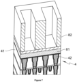
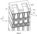
- THE figures 7 And 8 present a step of photolithography and etching of the first dielectric layer 81.
- the first dielectric layer 81 is etched through a temporary etching mask 82, with a stop on the material layer barrier 61, so as to form flanks 810 in the first dielectric layer 81.
- Each flank 810 is arranged directly above at least one via 42.
- the first dielectric layer 81 comprises four flanks 810, each of them extending along a column of vias 42 and directly above these vias 42.
- the first dielectric layer 81 also reveals the barrier material layer 61. This etching can be carried out using a fluorinated plasma.
- FIG. 9 presents a step of conformal deposition of a layer 520 of resistive material on the first dielectric layer 81, including the sides 810 of the latter, and the exposed parts of the barrier material layer 61.
- the resistive layer 520 is for example made from TiN, TiC, TiSiN, TiSiCN, TiWN, TaN or TaCN.
- FIG. 9 also presents the conformal deposition of a second dielectric layer 83, for example in SiN, on the resistive layer 520.
- the thickness of the second dielectric layer 83 makes it possible to control the extent of the foot 522 of the heating element 52 in the X direction.
- the absence of the second dielectric layer 83 makes it possible to avoid the appearance of the foot 522.
- its presence makes it possible to protect the integrity of the fin 521 during the etching of the resistive layer 520.
- FIG. 10 has a step of anisotropic etching of the second dielectric layer 83 and of the resistive layer 520.
- This etching is oriented perpendicular to the flat surface 410 of the substrate 41 (in other words along -Z) with a stop on the layer 62 of barrier material. It can be carried out using a fluorinated and chlorinated plasma. It delimits in particular the fins 521 of the resistive layer 520, extending against the flank 810 of the first dielectric layer 81, and the feet 522 of the resistive layer 520, protected from the anisotropic etching by a part of the second dielectric layer 83 having a significant height (the height being measured along the Z direction).
- the portions 521, 522 of the resistive layer thus extend directly above the vias 42 arranged in a column.
- FIG. 11 presents an anisotropic etching of the layer 61 in barrier material with stop on the substrate 41.
- This etching is carried out by using the first dielectric layer 81, the remaining parts of the second dielectric layer 83 and the fins 521 of the resistive layer 520 as a mask of etching.
- This etching makes it possible to delimit first strips 62 of barrier material in the layer 61 of barrier material.
- Each strip 62 extends against the contact surfaces 420 of vias 42 extending against two neighboring columns.
- the etching of the layer of barrier material is carried out so as to form the diffusion barrier(s) on the surface of the contact.
- the etchings of the second dielectric layer 83, the resistive layer 520 and the barrier material layer 61 can be carried out sequentially in the same step.
- the etching of the barrier material layer 61 can also be carried out using a fluorine and chlorine plasma.
- FIG. 12 has a conformal deposition of a third dielectric layer 84, for example in SiN, on all of the elements.
- This third dielectric layer 84 makes it possible to passivate the feet 522 of the resistive layer 520 (if they are present), intended to form the feet of the heating elements 52 of the memories 5.
- FIG 13 has an anisotropic etching, for example by means of a fluorine plasma, of the third dielectric layer 84 with a stop on the substrate 41.
- This etching removes the portions of the third dielectric layer 84 extending on the substrate 41 and joining two neighboring feet 522 of the resistive layer 520.
- it leaves portions extending perpendicular to the plane, against the remaining parts of the second dielectric layer 83 (themselves extending against the fins 521 of the resistive layer 520).
- FIG. 14 presents a step of filling the cavities exposing the substrate 41.
- the filling is for example carried out by the deposition of a fourth dielectric material 85, for example in SiO 2 , covering all of the elements.
- FIG. 15 presents a CMP planarization step allowing to expose a part of each fin 521 on which the first active layers 51 will be connected.
- the advantage of partially etching the third dielectric layer 84, as illustrated in the figure 13 is to remove the surface dielectric material which facilitates the CMP planarization of the Figure 15 . Indeed, it is simpler to planarize an oxide such as SiO 2 rather than a dielectric such as SiN. We then obtain a CMP planarization of the oxide which is selective and with stop on SiN controllable and reproducible in the sense of an industrializable process.
- FIG 16 presents a step of depositing the first active layer 51 against the fins 521 and against the dielectric layers 81, 83, 84, 85 deposited previously.
- the first active layer 51 extends parallel to the upper surface 410 of the substrate 41.
- FIG 16 also presents a step of depositing a first metal layer 53, intended to form the upper electrodes, on the first active layer 51.
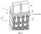
- FIG. 17 presents a step of depositing a second etching mask 86 on the first active layer 51 and the first metal layer 53.
- the second etching mask 86 has islands aligned with the rows and columns of vias 42, i.e. in the X and Y directions. Each island is arranged and oriented so as to delimit, after etching, the diffusion barriers 6 and the memories 5, 5'.
- each island is arranged and oriented so as to completely cover, by projection along Z, two neighboring vias 46 of the same row.
- each of the islands only completely covers, by projection along Z, a single via 46 of the same column. In this way, the islands expose portions of the resistive layer 520 and the strips 62 of barrier material to etching.
- the islands of the mask 86 are also distant from each other. In this case, the islands of the same line (aligned along X) have a separation perpendicular to each strip 62 of barrier material, exposing other portions of the latter to etching.
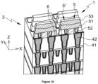
- the arrangement of the islands of the second mask 86 makes it possible to form, after etching, the non-volatile memories 5, 5' as illustrated by the Figures 1A And 1B
- Each island of the second etching mask 86, covering two vias 42 of the same line, makes it possible to form memories 5, 5' of the same line whose first active layers 51 and upper electrodes 53 are common.
- Etching through the second etching mask 86 also makes it possible to section the resistive layer 520 to delimit the heating elements 52 in the extension of each first active layer 51.
- THE figures 19 to 22 present complementary steps that can be implemented from cell 1 obtained by the step of the figure 18 . These additional steps make it possible to manufacture a selector, for example in OTS, for each 5.5" memory and connect each selector to a conductive track 7. They make it possible in particular to obtain circuit 1 of the Figure 3 .
- FIG 19 presents the formation of a second active layer 54 on each upper electrode 53.
- the second active layer 54 is for example deposited, during the step of the figure 16 , on the first metal layer 53.
- the etching of the Figure 17 makes it possible to obtain a plurality of memories 5, 5' with a first active layer 51, for example responsible for storing information, and a second active layer 54, intended to form a selection element (also called "selector") of the first active layer 51.
- the materials indicated previously can be used to produce this second active layer 54.
- a second metal layer 55 can also be deposited on the second active layer 54.
- FIG. 20 shows the encapsulation of the memories 5, 5' comprising the conformal deposition of a fifth dielectric layer 87 against the sides of each memory 5, 5' and the filling of the cavities left by the encapsulation by a sixth dielectric layer 88, for example in SiO 2 .
- the top of the memories 5, 5' is released by means of a CMP planarization step with stopping on the top of the memories 5, 5', i.e. the second metal layer 55.
- FIG. 21 shows the deposition of a third metal layer 71 allowing the conductive tracks 7 to be produced.
- FIG 22 presents a step of etching the third metal layer 71 and the different layers 51, 52, 53, 54, 55 of the memories 5, 5'.
- the etching is carried out through a third etching mask aligned on the columns of vias 42, with a stop on the substrate 41. This etching separates the memories 5, 5' from each other (i.e. the first and second layers 51, 54 are distinct), each being connected to a conductive track 7.
- a first variant of implementation of the method consists in replacing the deposition and the etchings aimed at forming the diffusion barriers 6 by a step of growth of said barriers 6.
- the growth of the barriers comprises for example a step of selective deposition with respect to the substrate 41.
- the materials used to carry out the selective deposition therefore comprise any type of material based on Ta, or Ti or Co and allowing selective deposition. These are for example so-called “ceramic” materials as presented previously (for example TaN/Ta, TiN, TiC, TiSiN, TiSiCN, TiWN, TaN or even TaCN) or metallic materials, such as titanium or tantalum or cobalt.
- the selective deposition of a compatible material with respect to the substrate 41 thus makes it possible to achieve the growth of the barriers from each contact surface 420 of the vias 42, opening onto the substrate 41. It is therefore no longer necessary to resort to an etching step to delimit and align the barriers 6 with the vias 42.
- THE figures 23 to 25 present a variant of implementation of the manufacturing process, in particular figures 16 to 18 . This variant allows to obtain the circuit of the Figure 2 .
- this variant proposes etching the stack of the Figure 15 through an etching mask, with a stop on the substrate 41.
- the result of the etching is illustrated by the figure 23 . It makes it possible to delimit each heating element 52 and each diffusion barrier 6 in the extension of one another.
- the etching mask used to carry out the etching is similar to the second etching mask 86 illustrated in the Figure 17 , including in particular islets.
- FIG 24 shows the result of a step of depositing a seventh dielectric layer 89, for example in SiN, and of a CMP planarization with stop at the top of the heating elements 52.
- FIG 25 shows circuit 1 obtained after depositing a first active layer on the stack of the figure 24 and etching the latter so as to form lines of first active layer 51, extending against the heating elements 52 of the same line.
Landscapes
- Engineering & Computer Science (AREA)
- Manufacturing & Machinery (AREA)
- Semiconductor Memories (AREA)
Applications Claiming Priority (1)
| Application Number | Priority Date | Filing Date | Title |
|---|---|---|---|
| FR2314206A FR3157057A1 (fr) | 2023-12-14 | 2023-12-14 | Circuit intégré comprenant une mémoire non volatile et procédé de fabrication associé |
Publications (1)
| Publication Number | Publication Date |
|---|---|
| EP4572595A1 true EP4572595A1 (de) | 2025-06-18 |
Family
ID=91829403
Family Applications (1)
| Application Number | Title | Priority Date | Filing Date |
|---|---|---|---|
| EP24307084.4A Pending EP4572595A1 (de) | 2023-12-14 | 2024-12-12 | Integrierte schaltung mit nichtflüchtigem speicher und herstellungsverfahren dafür |
Country Status (3)
| Country | Link |
|---|---|
| US (1) | US20250204286A1 (de) |
| EP (1) | EP4572595A1 (de) |
| FR (1) | FR3157057A1 (de) |
Citations (3)
| Publication number | Priority date | Publication date | Assignee | Title |
|---|---|---|---|---|
| US20090026437A1 (en) * | 2007-07-25 | 2009-01-29 | Yudong Kim | Copper compatible chalcogenide phase change memory with adjustable threshold voltage |
| US20190123273A1 (en) * | 2017-10-24 | 2019-04-25 | Samsung Electronics Co., Ltd. | Nonvolatile memory apparatus including resistive-change material layer |
| US20230074555A1 (en) * | 2021-08-25 | 2023-03-09 | International Business Machines Corporation | Phase change memory with heater |
-
2023
- 2023-12-14 FR FR2314206A patent/FR3157057A1/fr active Pending
-
2024
- 2024-12-12 EP EP24307084.4A patent/EP4572595A1/de active Pending
- 2024-12-13 US US18/980,511 patent/US20250204286A1/en active Pending
Patent Citations (3)
| Publication number | Priority date | Publication date | Assignee | Title |
|---|---|---|---|---|
| US20090026437A1 (en) * | 2007-07-25 | 2009-01-29 | Yudong Kim | Copper compatible chalcogenide phase change memory with adjustable threshold voltage |
| US20190123273A1 (en) * | 2017-10-24 | 2019-04-25 | Samsung Electronics Co., Ltd. | Nonvolatile memory apparatus including resistive-change material layer |
| US20230074555A1 (en) * | 2021-08-25 | 2023-03-09 | International Business Machines Corporation | Phase change memory with heater |
Non-Patent Citations (3)
Also Published As
| Publication number | Publication date |
|---|---|
| FR3157057A1 (fr) | 2025-06-20 |
| US20250204286A1 (en) | 2025-06-19 |
Similar Documents
| Publication | Publication Date | Title |
|---|---|---|
| CN101236985B (zh) | 一种具有共平面电极表面的存储单元装置及其制造方法 | |
| EP3750199B1 (de) | Dreidimensionaler widerstandsspeicher | |
| EP3863074B1 (de) | Speicherzelle mit phasenumwandlung | |
| EP2706583B1 (de) | Phasenwechselspeicherzelle | |
| EP3506377B1 (de) | Elementarzelle, umfassend einen widerstandsspeicher und ein auswahlelement, ebene und matrix von ebenen umfassend eine vielzahl solcher zellen sowie zugeordnetes herstellungsverfahren | |
| WO2021122358A1 (fr) | Cellule elementaire comportant une memoire resistive et un dispositif destine a former un selecteur, matrice de cellules, procedes de fabrication et d'initialisation associes | |
| FR3112018A1 (fr) | Isolation de cellules mémoire à changement de phase | |
| WO2018046683A1 (fr) | Cellule memoire non-volatile resistive a base d'oxyde et son procede de fabrication | |
| EP4572595A1 (de) | Integrierte schaltung mit nichtflüchtigem speicher und herstellungsverfahren dafür | |
| EP3890024B1 (de) | Elektronischer chip mit zwei phasenwechselspeichern und herstellungsverfahren | |
| EP3840049A1 (de) | Elementarzelle, die einen resistiven speicher umfasst, und entsprechendes initialisierungsverfahren | |
| EP4339952B1 (de) | Phasenwechselspeicherzelle | |
| FR3115931A1 (fr) | Mémoire à changement de phase | |
| EP3168885B1 (de) | Herstellungsverfahren eines pcram-speichers | |
| WO2003017362A1 (fr) | Circuit integre avec cellule memoire dram | |
| EP4454444B1 (de) | Anordnung mit mindestens zwei nichtflüchtigen resistiven speichern und einem selektor, matrix und zugehöriges herstellungsverfahren | |
| EP4472395B1 (de) | Elektronische vorrichtung | |
| EP2684228B1 (de) | Elektronische speichervorrichtung | |
| EP4572594A1 (de) | Nichtflüchtige speicherstruktur mit einem stapel angeordnet in einem via und einer leitung darüber | |
| EP4339951A1 (de) | Phasenwechselspeicherzelle | |
| FR3131437A1 (fr) | Ensemble comprenant au moins deux mémoires résistives non-volatiles et deux sélecteurs, matrice et procédé de fabrication associés | |
| EP4454442A1 (de) | Anordnung mit mindestens zwei wählern und zwei nichtflüchtigen resistiven speichern, zugehörige matrix und herstellungsverfahren | |
| FR2828764A1 (fr) | Circuit integre et son procede de fabrication, et cellule de memoire incorporant un tel circuit | |
| FR2979467A1 (fr) | Dispositif microelectronique dote de cellules memoires resistives empilees |
Legal Events
| Date | Code | Title | Description |
|---|---|---|---|
| PUAI | Public reference made under article 153(3) epc to a published international application that has entered the european phase |
Free format text: ORIGINAL CODE: 0009012 |
|
| STAA | Information on the status of an ep patent application or granted ep patent |
Free format text: STATUS: REQUEST FOR EXAMINATION WAS MADE |
|
| 17P | Request for examination filed |
Effective date: 20241212 |
|
| AK | Designated contracting states |
Kind code of ref document: A1 Designated state(s): AL AT BE BG CH CY CZ DE DK EE ES FI FR GB GR HR HU IE IS IT LI LT LU LV MC ME MK MT NL NO PL PT RO RS SE SI SK SM TR |