EP4576182A2 - Verfahren zur herstellung einer elektronischen vorrichtung - Google Patents
Verfahren zur herstellung einer elektronischen vorrichtung Download PDFInfo
- Publication number
- EP4576182A2 EP4576182A2 EP24218553.6A EP24218553A EP4576182A2 EP 4576182 A2 EP4576182 A2 EP 4576182A2 EP 24218553 A EP24218553 A EP 24218553A EP 4576182 A2 EP4576182 A2 EP 4576182A2
- Authority
- EP
- European Patent Office
- Prior art keywords
- handle
- layer
- face
- plate
- grooves
- Prior art date
- Legal status (The legal status is an assumption and is not a legal conclusion. Google has not performed a legal analysis and makes no representation as to the accuracy of the status listed.)
- Pending
Links
Images




Classifications
-
- H—ELECTRICITY
- H10—SEMICONDUCTOR DEVICES; ELECTRIC SOLID-STATE DEVICES NOT OTHERWISE PROVIDED FOR
- H10H—INORGANIC LIGHT-EMITTING SEMICONDUCTOR DEVICES HAVING POTENTIAL BARRIERS
- H10H29/00—Integrated devices, or assemblies of multiple devices, comprising at least one light-emitting semiconductor element covered by group H10H20/00
- H10H29/01—Manufacture or treatment
- H10H29/03—Manufacture or treatment using mass transfer of LEDs, e.g. by using liquid suspensions
-
- H—ELECTRICITY
- H10—SEMICONDUCTOR DEVICES; ELECTRIC SOLID-STATE DEVICES NOT OTHERWISE PROVIDED FOR
- H10H—INORGANIC LIGHT-EMITTING SEMICONDUCTOR DEVICES HAVING POTENTIAL BARRIERS
- H10H20/00—Individual inorganic light-emitting semiconductor devices having potential barriers, e.g. light-emitting diodes [LED]
- H10H20/01—Manufacture or treatment
- H10H20/011—Manufacture or treatment of bodies, e.g. forming semiconductor layers
- H10H20/018—Bonding of wafers
-
- H—ELECTRICITY
- H10—SEMICONDUCTOR DEVICES; ELECTRIC SOLID-STATE DEVICES NOT OTHERWISE PROVIDED FOR
- H10H—INORGANIC LIGHT-EMITTING SEMICONDUCTOR DEVICES HAVING POTENTIAL BARRIERS
- H10H20/00—Individual inorganic light-emitting semiconductor devices having potential barriers, e.g. light-emitting diodes [LED]
- H10H20/80—Constructional details
- H10H20/81—Bodies
- H10H20/817—Bodies characterised by the crystal structures or orientations, e.g. polycrystalline, amorphous or porous
- H10H20/818—Bodies characterised by the crystal structures or orientations, e.g. polycrystalline, amorphous or porous within the light-emitting regions
-
- H—ELECTRICITY
- H10—SEMICONDUCTOR DEVICES; ELECTRIC SOLID-STATE DEVICES NOT OTHERWISE PROVIDED FOR
- H10H—INORGANIC LIGHT-EMITTING SEMICONDUCTOR DEVICES HAVING POTENTIAL BARRIERS
- H10H20/00—Individual inorganic light-emitting semiconductor devices having potential barriers, e.g. light-emitting diodes [LED]
- H10H20/80—Constructional details
- H10H20/81—Bodies
- H10H20/819—Bodies characterised by their shape, e.g. curved or truncated substrates
-
- H—ELECTRICITY
- H10—SEMICONDUCTOR DEVICES; ELECTRIC SOLID-STATE DEVICES NOT OTHERWISE PROVIDED FOR
- H10H—INORGANIC LIGHT-EMITTING SEMICONDUCTOR DEVICES HAVING POTENTIAL BARRIERS
- H10H29/00—Integrated devices, or assemblies of multiple devices, comprising at least one light-emitting semiconductor element covered by group H10H20/00
- H10H29/20—Assemblies of multiple devices comprising at least one light-emitting semiconductor device covered by group H10H20/00
- H10H29/24—Assemblies of multiple devices comprising at least one light-emitting semiconductor device covered by group H10H20/00 comprising multiple light-emitting semiconductor devices
-
- H—ELECTRICITY
- H10—SEMICONDUCTOR DEVICES; ELECTRIC SOLID-STATE DEVICES NOT OTHERWISE PROVIDED FOR
- H10P—GENERIC PROCESSES OR APPARATUS FOR THE MANUFACTURE OR TREATMENT OF DEVICES COVERED BY CLASS H10
- H10P72/00—Handling or holding of wafers, substrates or devices during manufacture or treatment thereof
- H10P72/70—Handling or holding of wafers, substrates or devices during manufacture or treatment thereof for supporting or gripping
- H10P72/74—Handling or holding of wafers, substrates or devices during manufacture or treatment thereof for supporting or gripping using temporarily an auxiliary support
-
- H—ELECTRICITY
- H10—SEMICONDUCTOR DEVICES; ELECTRIC SOLID-STATE DEVICES NOT OTHERWISE PROVIDED FOR
- H10H—INORGANIC LIGHT-EMITTING SEMICONDUCTOR DEVICES HAVING POTENTIAL BARRIERS
- H10H20/00—Individual inorganic light-emitting semiconductor devices having potential barriers, e.g. light-emitting diodes [LED]
- H10H20/01—Manufacture or treatment
-
- H—ELECTRICITY
- H10—SEMICONDUCTOR DEVICES; ELECTRIC SOLID-STATE DEVICES NOT OTHERWISE PROVIDED FOR
- H10H—INORGANIC LIGHT-EMITTING SEMICONDUCTOR DEVICES HAVING POTENTIAL BARRIERS
- H10H20/00—Individual inorganic light-emitting semiconductor devices having potential barriers, e.g. light-emitting diodes [LED]
- H10H20/80—Constructional details
- H10H20/81—Bodies
- H10H20/813—Bodies having a plurality of light-emitting regions, e.g. multi-junction LEDs or light-emitting devices having photoluminescent regions within the bodies
-
- H—ELECTRICITY
- H10—SEMICONDUCTOR DEVICES; ELECTRIC SOLID-STATE DEVICES NOT OTHERWISE PROVIDED FOR
- H10H—INORGANIC LIGHT-EMITTING SEMICONDUCTOR DEVICES HAVING POTENTIAL BARRIERS
- H10H20/00—Individual inorganic light-emitting semiconductor devices having potential barriers, e.g. light-emitting diodes [LED]
- H10H20/80—Constructional details
- H10H20/81—Bodies
- H10H20/819—Bodies characterised by their shape, e.g. curved or truncated substrates
- H10H20/821—Bodies characterised by their shape, e.g. curved or truncated substrates of the light-emitting regions, e.g. non-planar junctions
-
- H—ELECTRICITY
- H10—SEMICONDUCTOR DEVICES; ELECTRIC SOLID-STATE DEVICES NOT OTHERWISE PROVIDED FOR
- H10H—INORGANIC LIGHT-EMITTING SEMICONDUCTOR DEVICES HAVING POTENTIAL BARRIERS
- H10H20/00—Individual inorganic light-emitting semiconductor devices having potential barriers, e.g. light-emitting diodes [LED]
- H10H20/80—Constructional details
- H10H20/85—Packages
- H10H20/857—Interconnections, e.g. lead-frames, bond wires or solder balls
-
- H—ELECTRICITY
- H10—SEMICONDUCTOR DEVICES; ELECTRIC SOLID-STATE DEVICES NOT OTHERWISE PROVIDED FOR
- H10P—GENERIC PROCESSES OR APPARATUS FOR THE MANUFACTURE OR TREATMENT OF DEVICES COVERED BY CLASS H10
- H10P72/00—Handling or holding of wafers, substrates or devices during manufacture or treatment thereof
- H10P72/70—Handling or holding of wafers, substrates or devices during manufacture or treatment thereof for supporting or gripping
- H10P72/74—Handling or holding of wafers, substrates or devices during manufacture or treatment thereof for supporting or gripping using temporarily an auxiliary support
- H10P72/7402—Wafer tapes, e.g. grinding or dicing support tapes
-
- H—ELECTRICITY
- H10—SEMICONDUCTOR DEVICES; ELECTRIC SOLID-STATE DEVICES NOT OTHERWISE PROVIDED FOR
- H10P—GENERIC PROCESSES OR APPARATUS FOR THE MANUFACTURE OR TREATMENT OF DEVICES COVERED BY CLASS H10
- H10P72/00—Handling or holding of wafers, substrates or devices during manufacture or treatment thereof
- H10P72/70—Handling or holding of wafers, substrates or devices during manufacture or treatment thereof for supporting or gripping
- H10P72/74—Handling or holding of wafers, substrates or devices during manufacture or treatment thereof for supporting or gripping using temporarily an auxiliary support
- H10P72/7408—Handling or holding of wafers, substrates or devices during manufacture or treatment thereof for supporting or gripping using temporarily an auxiliary support the auxiliary support including alignment aids
-
- H—ELECTRICITY
- H10—SEMICONDUCTOR DEVICES; ELECTRIC SOLID-STATE DEVICES NOT OTHERWISE PROVIDED FOR
- H10P—GENERIC PROCESSES OR APPARATUS FOR THE MANUFACTURE OR TREATMENT OF DEVICES COVERED BY CLASS H10
- H10P72/00—Handling or holding of wafers, substrates or devices during manufacture or treatment thereof
- H10P72/70—Handling or holding of wafers, substrates or devices during manufacture or treatment thereof for supporting or gripping
- H10P72/74—Handling or holding of wafers, substrates or devices during manufacture or treatment thereof for supporting or gripping using temporarily an auxiliary support
- H10P72/7416—Handling or holding of wafers, substrates or devices during manufacture or treatment thereof for supporting or gripping using temporarily an auxiliary support used during dicing or grinding
-
- H—ELECTRICITY
- H10—SEMICONDUCTOR DEVICES; ELECTRIC SOLID-STATE DEVICES NOT OTHERWISE PROVIDED FOR
- H10P—GENERIC PROCESSES OR APPARATUS FOR THE MANUFACTURE OR TREATMENT OF DEVICES COVERED BY CLASS H10
- H10P72/00—Handling or holding of wafers, substrates or devices during manufacture or treatment thereof
- H10P72/70—Handling or holding of wafers, substrates or devices during manufacture or treatment thereof for supporting or gripping
- H10P72/74—Handling or holding of wafers, substrates or devices during manufacture or treatment thereof for supporting or gripping using temporarily an auxiliary support
- H10P72/7426—Handling or holding of wafers, substrates or devices during manufacture or treatment thereof for supporting or gripping using temporarily an auxiliary support used as a support during build up manufacturing of active devices
-
- H—ELECTRICITY
- H10—SEMICONDUCTOR DEVICES; ELECTRIC SOLID-STATE DEVICES NOT OTHERWISE PROVIDED FOR
- H10P—GENERIC PROCESSES OR APPARATUS FOR THE MANUFACTURE OR TREATMENT OF DEVICES COVERED BY CLASS H10
- H10P72/00—Handling or holding of wafers, substrates or devices during manufacture or treatment thereof
- H10P72/70—Handling or holding of wafers, substrates or devices during manufacture or treatment thereof for supporting or gripping
- H10P72/74—Handling or holding of wafers, substrates or devices during manufacture or treatment thereof for supporting or gripping using temporarily an auxiliary support
- H10P72/7428—Handling or holding of wafers, substrates or devices during manufacture or treatment thereof for supporting or gripping using temporarily an auxiliary support used to support diced chips prior to mounting
-
- H—ELECTRICITY
- H10—SEMICONDUCTOR DEVICES; ELECTRIC SOLID-STATE DEVICES NOT OTHERWISE PROVIDED FOR
- H10P—GENERIC PROCESSES OR APPARATUS FOR THE MANUFACTURE OR TREATMENT OF DEVICES COVERED BY CLASS H10
- H10P72/00—Handling or holding of wafers, substrates or devices during manufacture or treatment thereof
- H10P72/70—Handling or holding of wafers, substrates or devices during manufacture or treatment thereof for supporting or gripping
- H10P72/74—Handling or holding of wafers, substrates or devices during manufacture or treatment thereof for supporting or gripping using temporarily an auxiliary support
- H10P72/7432—Handling or holding of wafers, substrates or devices during manufacture or treatment thereof for supporting or gripping using temporarily an auxiliary support used in a transfer process involving transfer directly from an origin substrate to a target substrate without use of an intermediate handle substrate
-
- H—ELECTRICITY
- H10—SEMICONDUCTOR DEVICES; ELECTRIC SOLID-STATE DEVICES NOT OTHERWISE PROVIDED FOR
- H10P—GENERIC PROCESSES OR APPARATUS FOR THE MANUFACTURE OR TREATMENT OF DEVICES COVERED BY CLASS H10
- H10P72/00—Handling or holding of wafers, substrates or devices during manufacture or treatment thereof
- H10P72/70—Handling or holding of wafers, substrates or devices during manufacture or treatment thereof for supporting or gripping
- H10P72/74—Handling or holding of wafers, substrates or devices during manufacture or treatment thereof for supporting or gripping using temporarily an auxiliary support
- H10P72/7434—Handling or holding of wafers, substrates or devices during manufacture or treatment thereof for supporting or gripping using temporarily an auxiliary support used in a transfer process involving at least two transfer steps, i.e. including an intermediate handle substrate
-
- H—ELECTRICITY
- H10—SEMICONDUCTOR DEVICES; ELECTRIC SOLID-STATE DEVICES NOT OTHERWISE PROVIDED FOR
- H10P—GENERIC PROCESSES OR APPARATUS FOR THE MANUFACTURE OR TREATMENT OF DEVICES COVERED BY CLASS H10
- H10P72/00—Handling or holding of wafers, substrates or devices during manufacture or treatment thereof
- H10P72/70—Handling or holding of wafers, substrates or devices during manufacture or treatment thereof for supporting or gripping
- H10P72/74—Handling or holding of wafers, substrates or devices during manufacture or treatment thereof for supporting or gripping using temporarily an auxiliary support
- H10P72/7438—Handling or holding of wafers, substrates or devices during manufacture or treatment thereof for supporting or gripping using temporarily an auxiliary support with parts of the auxiliary support remaining in the finished device
-
- H—ELECTRICITY
- H10—SEMICONDUCTOR DEVICES; ELECTRIC SOLID-STATE DEVICES NOT OTHERWISE PROVIDED FOR
- H10P—GENERIC PROCESSES OR APPARATUS FOR THE MANUFACTURE OR TREATMENT OF DEVICES COVERED BY CLASS H10
- H10P72/00—Handling or holding of wafers, substrates or devices during manufacture or treatment thereof
- H10P72/70—Handling or holding of wafers, substrates or devices during manufacture or treatment thereof for supporting or gripping
- H10P72/74—Handling or holding of wafers, substrates or devices during manufacture or treatment thereof for supporting or gripping using temporarily an auxiliary support
- H10P72/744—Details of chemical or physical process used for separating the auxiliary support from a device or a wafer
-
- H—ELECTRICITY
- H10—SEMICONDUCTOR DEVICES; ELECTRIC SOLID-STATE DEVICES NOT OTHERWISE PROVIDED FOR
- H10W—GENERIC PACKAGES, INTERCONNECTIONS, CONNECTORS OR OTHER CONSTRUCTIONAL DETAILS OF DEVICES COVERED BY CLASS H10
- H10W46/00—Marks applied to devices, e.g. for alignment or identification
-
- H—ELECTRICITY
- H10—SEMICONDUCTOR DEVICES; ELECTRIC SOLID-STATE DEVICES NOT OTHERWISE PROVIDED FOR
- H10W—GENERIC PACKAGES, INTERCONNECTIONS, CONNECTORS OR OTHER CONSTRUCTIONAL DETAILS OF DEVICES COVERED BY CLASS H10
- H10W46/00—Marks applied to devices, e.g. for alignment or identification
- H10W46/301—Marks applied to devices, e.g. for alignment or identification for alignment
-
- H—ELECTRICITY
- H10—SEMICONDUCTOR DEVICES; ELECTRIC SOLID-STATE DEVICES NOT OTHERWISE PROVIDED FOR
- H10W—GENERIC PACKAGES, INTERCONNECTIONS, CONNECTORS OR OTHER CONSTRUCTIONAL DETAILS OF DEVICES COVERED BY CLASS H10
- H10W46/00—Marks applied to devices, e.g. for alignment or identification
- H10W46/501—Marks applied to devices, e.g. for alignment or identification for use before dicing
Definitions
- This description relates generally to methods of manufacturing electronic devices, in particular optoelectronic devices comprising light-emitting diodes.
- An example of a method for manufacturing an electronic device includes forming, on a support, a plate comprising a plurality of copies of the electronic device followed by separating the electronic devices.
- the separation of the electronic devices may be achieved by cutting the plate and the support, in particular by sawing. Such a cutting method may be difficult to implement when the electronic devices each occupy a small area.
- a method for separating electronic devices to obtain cut lines of reduced width includes locally embrittling the support by laser treatment allowing the support to be broken by mechanical action to separate the electronic devices.
- a disadvantage is that the laser treatment can damage components of the electronic devices close to the cut lines. This disadvantage can be particularly pronounced when the electronic devices each include a plurality of three-dimensional semiconductor elements of nanometer or micrometer size, separated by an electrically insulating material. Indeed, since the size of the semiconductor three-dimensional elements and the distance separating the semiconductor three-dimensional elements are reduced, the heat dissipation of the heat provided by the laser processing can cause damage to the semiconductor three-dimensional elements close to the cutting lines.
- An embodiment overcomes all or part of the drawbacks of known electronic device manufacturing methods.
- An object of an embodiment is that components of electronic devices near the cutting lines are not damaged.
- the first handle is thinned to facilitate its breakage.
- the steps of forming the grooves and thinning the first handle do not damage the electronic devices of the plate since these steps are carried out before the fixing of the plate to the first handle.
- the fixing of the plate to the second face of the first handle obtained is carried out after thinning the first handle, it can then be obtained more easily, at the end of the thinning step, a surface condition of the second face suitable for the step of fixing the plate to the first handle. Better control of the quality of the fixing of the plate to the first handle can advantageously be obtained.
- the formation of the trenches in the plate in the extension of the grooves, and the breaking of the first handle at the trenches facilitates the separation of the electronic devices without damaging the electronic components of the electronic devices.
- the grooves are formed by laser engraving.
- the laser treatment does not damage the electronic components of the electronic devices since it is carried out before the plate is fixed to the first handle.
- the attachment of the first handle to the second handle is carried out by gluing with a first layer of glue.
- the first layer of glue advantageously allows for temporary bonding between the first handle and the second handle. This means that the first handle is attached to the second handle by the layer of glue and can then be easily detached from the second handle.
- the first layer of glue is located on the side of the first face of the first handle while the step of thinning the first handle is carried out on the side of the second face of the first handle.
- the first layer of glue does not interfere with the implementation of the thinning step.
- the first layer of glue does not interfere with the operation of a grinding or polishing tool used during the thinning step and is compatible with the thinning techniques so as to maintain the bonding.
- a surface condition of the second face suitable for the step of fixing for example by gluing, the plate to the first handle.
- Better control of the quality of the fixing, for example by gluing, of the plate to the first handle can advantageously be obtained.
- the step of removing the second handle further comprises a step of removing, totally or partially, the first layer of glue.
- the plate is fixed to the first handle by gluing with a second layer of glue.
- the bonding between the plate and the first handle is a permanent bond.
- the properties of the second layer of glue may therefore be different from the properties of the first layer of glue.
- the plate is fixed to the first handle by molecular bonding. This advantageously avoids the presence of the second layer of glue.
- the trenches are formed by etching the plate by dry etching or wet etching.
- the step of attaching the plate to the first handle comprises a step of positioning first marks of the first handle relative to second marks of the plate, such that each electronic device to be separated is positioned between four of the grooves.
- the first handle is at least partly made of glass, quartz, or sapphire.
- one of the grooves is located between each pair of adjacent electronic devices.
- the structure further comprises a first layer of glue between the first handle and the second handle.
- the structure further comprises a second layer of glue between the plate and the first handle.
- one of the grooves is located between each pair of adjacent electronic devices.
- the grooves delimit pads in the first handle, each pad facing only one of the electronic devices.
- An embodiment also provides an electronic system comprising an electronic device having a first sidewall and a block having first and second opposing faces and a second sidewall, the electronic device being attached to the second face, the electronic system further comprising flanks containing the first sidewall, the second sidewall and a portion connecting the first sidewall to the second sidewall projecting relative to the first sidewall and relative to the second sidewall.
- the electronic device comprises light-emitting diodes.
- the formation of the grooves advantageously does not cause deterioration of the light-emitting diodes adjacent to the desired cutting lines.
- each light-emitting diode comprises a three-dimensional semiconductor element of nanometric or micrometric size, corresponding to a microwire, a nanowire or a structure of nanometric or micrometric size of pyramidal shape, and an active layer covering the three-dimensional semiconductor element.
- the expressions “approximately”, “approximately”, “substantially”, and “of the order of” mean to within 10%, preferably to within 5%. In the case of angle, the expressions “about”, “approximately”, “substantially”, and “of the order of” mean to within 10°, preferably to within 5°.
- the terms “insulator” and “conductor” are considered here to mean “electrically insulating” and “electrically conducting” respectively.
- Optoelectronic devices are devices suitable for converting an electrical signal into electromagnetic radiation or vice versa, and in particular devices dedicated to the detection, measurement or emission of electromagnetic radiation.
- the transmittance of a layer corresponds to the ratio between the intensity of the radiation leaving the layer through an exit face and the intensity of the radiation entering the layer through an entry face opposite the exit face.
- a layer or film is said to be opaque to radiation when the transmittance of the radiation through the layer or film is less than 10%.
- a layer or film is said to be transparent to radiation when the transmittance of the radiation through the layer or film is greater than 10%.
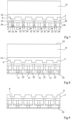
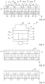
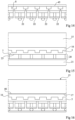
- FIG. 1A there Figure 2A , there Figure 3 , there Figure 4 , there Figure 5 , there Figure 6 , there Figure 7 , there figure 8 , there Figure 9 and the Figure 10 are partial and schematic sectional views of the structure obtained at stages of an embodiment of a method of manufacturing an electronic device.
- FIG. 1A is a partial and schematic sectional view of the structure obtained after a formation step in a first handle 5, comprising two opposite faces 6, 7, of grooves 8 extending from the face 6, eight grooves 8 being shown as an example in figure 1A .
- the faces 6 and 7 are parallel.
- the faces 6 and 7 are flat.
- the thickness of the first handle 5, outside the grooves 8, is between 50 ⁇ m and 3 mm.
- the first handle 5 has a single-layer or multi-layer structure.
- the first handle 5 is transparent to visible light.
- the first handle 5 is made of glass, quartz, or sapphire.
- the grooves 8 are rectilinear.
- Each groove 8 is characterized by a depth and a width. It typically comprises a bottom 9 and side walls 10. Depending on the section of the groove 8, the bottom 9 may be rounded or even disappear if the side walls 10 are in the shape of a "V". According to one embodiment, each groove 8 extends into the first handle 5, from the face 6 of the first handle 5, over a depth of between 5 ⁇ m and 200 ⁇ m, for example equal to approximately 30 ⁇ m. According to one embodiment, each groove 8 has a width of between 1 ⁇ m and 100 ⁇ m.
- FIG. 1B is a figure analogous to the Figure 1A and illustrates grooves 8 each having a "V" shaped cross section with inclined side walls 10.
- the grooves 8 delimit studs 11 in the first handle 5 separated from each other.
- the grooves 8 are formed by laser engraving, by chemical etching (wet or dry), by mechanical sawing or by a combination of these different techniques.
- the wavelength of the laser beam used to engrave the grooves 8 is between 100 nm and 3000 nm depending on the material to be engraved.
- the laser beam is emitted in the form of a pulse, of two or more pulses, each pulse having a duration between 0.1 ps and 1000 ps.
- the laser beam energy for each pulse is between 1 pJ and 100 pJ.
- FIG. 2A is a partial and schematic sectional view of the structure obtained after fixing a second handle 15 to the first handle 5 by means of a layer of glue 16 which allows temporary bonding of the second handle to the first handle.
- the second handle 15 is fixed to the first handle 5 on the side of the face 6, that is to say on the side of the grooves 8.
- the glue penetrates into the grooves 8.
- the second handle 15 comprises two opposite faces 17, 18, the layer of glue 16 being in direct physical contact with the face 17.
- the faces 17 and 18 are parallel.
- the faces 17 and 18 are planar.
- the thickness of the second handle 15 is between 50 ⁇ m and 3 mm.
- the second handle 15 is made of silicon or other semiconductor material, glass, quartz or sapphire.
- FIG. 2B is a figure analogous to the Figure 2A and illustrates a variant in which the layer of glue 16 does not penetrate into the grooves 8.
- the thickness of the adhesive layer 16 is between 10 ⁇ m and 300 ⁇ m.
- the adhesive layer 16 is made of an organic or inorganic matrix material having adhesion properties and detachment properties. This material may be a composite, a single layer or a multi-layer material.
- FIG. 3 is a partial and schematic sectional view of the structure obtained after a step of thinning the first handle 5 from the face 7.
- the thinning step can be carried out by grinding and/or by CMP (English acronym for Chemical-Mechanical Polishing).
- the CMP step can comprise, simultaneously or successively, mechanical polishing steps and chemical etching steps.
- the thickness of the first handle 5 is between 30 ⁇ m and 200 ⁇ m.
- the thickness of the first handle 5 at the bottom of each groove 8 is sufficiently low to allow the implementation of a breaking step of the first handle 5 at the bottom of each groove 8 at a later step of the method described below and is sufficiently high to prevent accidental breaking of the first handle 5 at the bottom of one of the grooves 8 before the implementation of the breaking step, even if the first handle 5 may be subjected to bending during the steps of the method.
- the layer of glue 16 is located on the side of the face 6 of the first handle 5 while the thinning step is carried out on the side of the face 7 of the first handle 5.
- the layer of glue 16 does not hinder the implementation of the thinning step.
- the layer of glue 16 does not hinder the operation of a grinding or polishing tool used during the thinning step.
- FIG. 4 is a partial and schematic sectional view of the structure obtained after the manufacture of a plate 20 on a substrate 21, the plate 20 comprising several examples of an electronic device 22, four examples of the electronic device 22 being represented in their entirety by way of example in Figure 4 .
- the plate 20 comprises an upper face 23 and a lower face 24, opposite the upper face 23.
- the lower face 24 is in contact with the substrate 21.
- the upper face 23 is preferably flat.
- the thickness of the plate 20 is between 1 ⁇ m and 100 ⁇ m, preferably between 10 ⁇ m and 20 ⁇ m.
- the electronic device 22 comprises at least one electronic component 25, a single electronic component 25 being represented very schematically as an example for each electronic device 22 in Figure 4 .
- the electronic device 22 is an optoelectronic device.
- the electronic components 25 can then comprise light sources, in particular light-emitting diodes.
- FIG. 5 is a partial and schematic sectional view of the structure obtained after fixing the plate 20 to the first handle 5. More precisely, the upper face 23 of the plate 20 is fixed to the face 7 of the first handle 5, that is to say on the side opposite the grooves 8. According to one embodiment, the plate 20 is fixed to the first handle 5 by means of a layer of glue 30.
- the layer of glue 30 is made of an organic or inorganic matrix material having adhesion properties and optical properties allowing transmission of light in the visible spectrum, and is for example made of an epoxy-based material, in particular a photosensitive resin of the SU-8 type, a benzocyclobutene (BCB)-based resin, an optical adhesive marketed under the name NOA or even under the name IBA.
- This material can be a composite, a single layer or a multi-layer material.
- the thickness of the adhesive layer 30 is between 1 ⁇ m and 40 ⁇ m.
- the adhesive layer 30 corresponds to an optical adhesive.
- the adhesive layer 30 may be transparent to the radiation of the light-emitting diode.
- the adhesive layer 16 does not hinder the implementation of the step of thinning the first handle 5. It can then be obtained more easily, at the end of the thinning step, a surface state of the face 7 suitable for the step of fixing, for example by gluing, the plate 20 to the first handle 5. Better control of the quality of the fixing, for example by gluing, of the plate 20 to the first handle 5 can advantageously be obtained.
- the grooves 8 are located in the extension of desired cutting lines between the electronic devices 22.
- the cutting lines are indicated schematically by lines 29 in dashed lines in Figure 5
- the desired cutting lines 29 between the electronic devices 22 and the grooves 8 are superimposed in a direction orthogonal to the face 7, the desired cutting lines 29 covering the grooves 8 in a direction orthogonal to the face 7.
- the cutting lines 29 are opposite the pattern formed by the grooves 8 in a direction orthogonal to the face 7.
- the cutting lines 29 correspond to the parts of the plate 20 to be removed to obtain the separation of the electronic devices 22.
- the correct positioning of the plate 20 relative to the first handle 5 is obtained by using for example marks on the plate 20 and marks on the first handle 5 (the marks not being illustrated).
- the electronic component 25 or the electronic components 25 of each electronic device 22 are surrounded by the grooves 8. This means, in projection in a plane parallel to the face 7, a groove 8 is located between the electronic component 25 or the components electronics 25 of each electronic device 22 of two adjacent electronic devices 22. Each pad 11 is thus opposite only one of the electronic devices 22.
- FIG. 6 is a partial and schematic sectional view of the structure obtained after removal of the substrate 21 to expose the lower face 24 of the plate 20 and after a step of forming, on the face 24 of the plate 20, electrical connection elements of the electronic devices 22, for example solder balls 31 or connection pads.
- the step of removing the substrate 21 is carried out for example by grinding, by dry etching, in particular plasma etching, or by wet etching, or by chemical-mechanical polishing, also called CMP (English acronym for Chemical-Mechanical Polishing).
- FIG. 7 is a partial and schematic sectional view of the structure obtained after the formation of trenches 32 in the plate 20, and possibly in the glue layer 30, to delimit the electronic devices 22 to be separated.
- the trenches 32 are formed on the desired cutting lines 29 between the electronic devices 22.
- Each trench 32 comprises a bottom 33 and side walls 34.
- the trenches 32 may extend into the glue layer 30 until they reach the face 7 of the first handle 5.
- the trenches 32 do not extend into the first handle 5.
- the bottom 33 of the trench 32 corresponds to a portion of the face 7 of the first handle 5.
- the depth of each trench 32 is between 10 ⁇ m and 80 ⁇ m.
- the adhesive film 35 is made of a material included in the group comprising the materials described in the patents US 4222913 And US 4379197 , polyethylene resins without polymerized vinyl acetate groups, acrylate polymers such as the following components: 2-ethylhexyl acrylate, n-butyl acrylate, methyl acrylate and t-butyl methacrylate.
- a stretchable material is defined as a material whose longitudinal deformation modulus, i.e. the ratio between the stress and the relative elongation, is between 102 Pa and 106 Pa.
- the film 35 is adapted to deform with an elongation at the breaking limit greater than 150%, preferably greater than 300%.
- FIG. 9 is a partial and schematic sectional view of the structure obtained after the removal of the second handle 15 and the removal of the glue layer 16 to expose the face 6 and the grooves 8 of the first handle 5.
- the glue layer 16 may not be removed completely but only partially.
- the first handle 5 which forms a continuous screen advantageously plays a role in protecting the electronic devices 22 during the removal of the second handle 15 and the removal, total or partial, of the glue layer 16.
- the material composing the glue layer 16 allows temporary bonding to be created between the first handle 5 and the second handle. 15. This means that the mechanical connection provided by the layer of glue 16 between the first handle 5 and the second handle 15 can be broken by a treatment which does not damage the other elements of the structure, in particular the first handle 5, the second handle 15, and the plate 20.
- the removal or physicochemical modification of the glue layer 16 is carried out by degradation of the material composing the glue layer 16.
- the degradation of the material composing the glue layer 16 is carried out by heating the glue layer 16.
- the degradation of the material composing the glue layer 16 is carried out by a chemical action on the glue layer 16, carried out simultaneously with the heating of the glue layer 16.
- the degradation of the material composing the glue layer 16 is carried out by exposing the glue layer 16 to radiation, for example ultraviolet, infrared, or visible light radiation, possibly from a laser source.
- the second handle 15 is removed by grinding and/or by CMP (English acronym for Chemical-Mechanical Polishing) of the second handle 15 from the face 18.
- CMP Chemical-Mechanical Polishing
- the adhesive layer 16 can then be removed by using a solvent, by wet or dry etching, or by plasma incineration.
- FIG. 10 is a partial and schematic sectional view of the structure obtained after mechanical rupture of the first handle 5 from the bottom 9 of each groove 8.
- the mechanical rupture is carried out by mechanical devices which produce the fracture between the grooves 8 and the trenches 32 in the thin layer of material remaining of the first handle 5 between the bottom 9 of the grooves 8 and the bottom of the trenches 32.
- the first handle 5 is then separated into blocks 36, each block 36 being fixed to one of the electronic devices 22.
- the rupture zones 37 extend from the bottom 9 of each groove 8 to the face 7 of the first handle 5 in the bottom 33 of the trench 32 located in the extension of the groove 8.
- Separate electronic systems 40 are thus obtained, each electronic system 40 comprising the electronic device 22 and the block 36 to which it is fixed.
- the breaking step comprises extending the adhesive film 35 in the plane of the adhesive film 35, the electronic devices 22 then being separated but still attached to the adhesive film 35, the adhesive film 35 being in a stretched state, i.e. tensile forces are exerted on the adhesive film such that the surface area of the stretched adhesive film in top view corresponds to 150% to 10000% of the surface area of the same adhesive film on which tensile forces are not exerted.
- the stretched state of the adhesive film is maintained by mechanical means.
- the electronic systems 40 can then be handled separately, for example by a pick and place system, not shown, and detached from the adhesive film 35.
- the method may include subsequent steps, in particular a step of removing the blocks 36 and the layer of glue 30 present under each electronic device 22.
- the block 36 may advantageously be transparent to the light radiation emitted by the electronic device 22.
- the embodiment of the manufacturing method advantageously allows the laser treatment of the first handle 5 to form the grooves 8 not to damage the electronic components 25 of the plate 20 since the laser treatment of the first handle 5 is carried out before the plate 20 is fixed to the first handle 5.
- FIG 11 is a partial and schematic sectional view of an electronic system 40 of the Figure 10 .
- the electronic system 40 comprises the electronic device 22 and the block 36 to which it is fixed by a portion of the adhesive layer 30.
- the electronic system 40 comprises sides 41, each side 41 comprising the side wall 34 of the trench 32 having allowed the delimitation of the electronic device 22, a part of the bottom 33 of this trench 32, a side wall 10 of the groove 8 which was located in the extension of the trench 32, a part of the bottom 9 of the groove 8, and a wall 42 resulting from the rupture of the first handle 5.
- the wall 42 projects laterally relative to the wall 34 of the electronic device 22.
- the wall 34 is not coplanar with the wall 10.
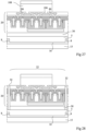
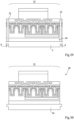
- FIG. 12 there figure 13 and the Figure 14 are partial and schematic sectional views of structures obtained in steps of another embodiment of a method of manufacturing an electronic device.
- FIG 12 is a partial and schematic sectional view of the structure obtained after fixing an adhesive film 45, made of stretchable material, to the structure obtained in Figure 9 on the side of the first handle 5, more precisely on the side of face 6 of the first handle 5.
- FIG. 13 is a partial and schematic sectional view of the structure obtained after removal of the adhesive film 35.
- the breaking step comprises extending the adhesive film 45 in the plane of the adhesive film 45, the electronic devices 22 then being separated but still attached to the adhesive film 45 in a stretched state.
- the electronic systems 40 can then be handled separately, for example by a pick and place system, not shown, and detached from the adhesive film 45.
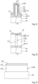
- FIG. 15 is a partial and schematic sectional view of the structure obtained in a step of another embodiment of a method of manufacturing an electronic device.
- the manufacturing method according to the present embodiment comprises the steps described previously in relation to the figures 1 to 10 with the difference that the plate 20 is fixed to the first handle 5 by molecular bonding in which the face 23 of the plate 20 is placed in direct physical contact with the face 7 of the first handle 5 without the interposition of an additional bonding material.
- FIG 16 is a partial and schematic sectional view of the structure obtained in a step of another embodiment of a method of manufacturing an electronic device.
- the manufacturing method according to the present embodiment comprises the steps described previously in relation to the figures 1 to 10 with the difference that the second handle 15 comprises a sacrificial layer 46 on the side of the face 17, for example in contact with the layer of glue 16.
- the sacrificial layer 46 which is degraded, for example by laser treatment, to allow the removal of the second handle 15, and the glue layer 16 is then removed, for example by chemical etching.
- the first handle 5 has a multilayer structure and comprises a layer 50 of a first material covering a substrate 52 made of a second material different from the first material.
- the grooves 8 are formed in the layer 50.
- the substrate 52 may be transparent to the laser.
- the second material is a semiconductor material.
- the semiconductor material may be silicon, germanium or a mixture of at least two of these compounds.
- the substrate 52 is made of silicon, more preferably monocrystalline silicon.
- the substrate 52 may be, at least in part, of a non-semiconductor material, for example an electrically insulating material or an electrically conductive material.
- the thickness of the layer 50 is between 50 ⁇ m and 200 ⁇ m.
- the second material composing the substrate 52 is chosen to facilitate the thinning step described previously in relation to the Figure 3 . In particular, the determination of the end of the stage thinning is facilitated since it corresponds to the complete removal of the substrate 52.
- the first material is transparent to visible light.
- the first material comprises glass, quartz, and sapphire.
- the electronic device 22 is an optoelectronic device and the electronic components 25 comprise light-emitting diodes comprising three-dimensional semiconductor elements of nanometric or micrometric size, in particular microwires or nanowires or pyramid-shaped structures covered with active layers.
- the electronic components 25 comprise light-emitting diodes comprising three-dimensional semiconductor elements of nanometric or micrometric size, in particular microwires or nanowires or pyramid-shaped structures covered with active layers.
- microwire designates a three-dimensional structure of elongated shape in a preferred direction of which at least two dimensions, called minor dimensions, are between 5 nm and 5 ⁇ m, preferably between 100 nm and 2 ⁇ m, more preferably between 200 nm and 1.5 ⁇ m, the third dimension, called major dimension or height, being greater than or equal to 1 time, preferably greater than or equal to 3 times and even more preferably greater than or equal to 5 times, the largest of the minor dimensions.
- the height of each microwire or nanowire may be greater than or equal to 500 nm, preferably between 1 ⁇ m and 50 ⁇ m.
- the term "wire” is used to mean “microwire or nanowire”.
- the cross-section of the wires may have various shapes, for example, an oval, circular or polygonal shape, including triangular, rectangular, square or hexagonal. It will be understood that the term "average diameter" used in relation to a cross-section of a wire means a quantity associated with the area of the wire in this cross-section, corresponding, for example, to the diameter of the disc having the same area as the cross-section of the wire.
- pyramid designates a three-dimensional structure, part of which is pyramidal or elongated conical in shape.
- This pyramidal structure may be truncated, i.e. the top of the cone is absent, leaving a plateau.
- the base of the pyramid is inscribed in a square whose side dimensions are from 100 nm to 10 ⁇ m, preferably between 0.2 ⁇ m and 2 ⁇ m.
- the polygon forming the base of the pyramid may be a hexagon.
- the height of the pyramid between the base of the pyramid and the apex or summit plateau varies from 100 nm to 20 ⁇ m, preferably between 200 nm and 2 ⁇ m.
- the wires comprise in majority, preferably more than 60% by mass, more preferably more than 80% by mass, at least one semiconductor material.
- the semiconductor material may be silicon, germanium, silicon carbide, a III-V compound, a II-VI compound or a combination of at least two of these compounds.
- group III elements include gallium (Ga), indium (In), or aluminum (Al).
- III-N compounds are GaN, AlN, InN, InGaN, AlGaN, or AlInGaN.
- Other group V elements may also be used, for example, phosphorus or arsenic.
- the elements in the III-V compound may be combined with different mole fractions.
- group II elements include group IIA elements, including beryllium (Be) and magnesium (Mg), and group IIB elements, including zinc (Zn), cadmium (Cd), and mercury (Hg).
- group VI elements include group VIA elements, including oxygen (O) and tellurium (Te).
- II-VI compounds are ZnO, ZnMgO, CdZnO, CdZnMgO, CdHgTe, CdTe or HgTe.
- the elements in the II-VI compound can be combined with different mole fractions.
- the semiconductor material of the wires can have a dopant, for example silicon providing N-type doping of a III-N compound, or magnesium providing P-type doping of a III-N compound.
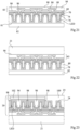
- FIG 18 there figure 18 , there figure 19 , there figure 20 , there figure 21 , there figure 22 , and the figure 23 illustrate the fabrication of the plate 20 on the substrate 21 in the case where the plate 20 comprises several copies of the optoelectronic device 22 with nanowires or microwires.
- FIG 24 is a partial and schematic sectional view illustrating the step described above in relation to the Figure 5 comprising the fixing by gluing of the face 23 of the plate 20 to the first handle 5 by the layer of glue 30.
- the first handle 5 is shown here with two grooves 8.
- FIG 27 is a partial and schematic sectional view of the structure obtained after a step of forming conductive pads 108 in contact with the conductive tracks 86 exposed through the openings 106, a single conductive pad 108 being shown as an example in figure 27 .
- Each conductive pad 108 may have a single-layer or multi-layer structure.
- the substrate 60 may correspond to a single-piece structure or correspond to a layer covering a support made of another material.
- the substrate 60 is preferably a semiconductor substrate, for example a substrate made of silicon, germanium, silicon carbide, a III-V compound, such as GaN or GaAs, or a ZnO substrate.
- the substrate 60 is a monocrystalline silicon substrate.
- the substrate 60 may correspond to a multilayer structure of the silicon-on-insulator type, also called SOI (English acronym for Silicon On Insulator).
Landscapes
- Casings For Electric Apparatus (AREA)
- Led Devices (AREA)
- Drying Of Semiconductors (AREA)
Applications Claiming Priority (1)
| Application Number | Priority Date | Filing Date | Title |
|---|---|---|---|
| FR2315024A FR3157659A1 (fr) | 2023-12-22 | 2023-12-22 | Procede de fabrication d'un dispositif electronique |
Publications (2)
| Publication Number | Publication Date |
|---|---|
| EP4576182A2 true EP4576182A2 (de) | 2025-06-25 |
| EP4576182A3 EP4576182A3 (de) | 2025-08-13 |
Family
ID=91738927
Family Applications (1)
| Application Number | Title | Priority Date | Filing Date |
|---|---|---|---|
| EP24218553.6A Pending EP4576182A3 (de) | 2023-12-22 | 2024-12-10 | Verfahren zur herstellung einer elektronischen vorrichtung |
Country Status (3)
| Country | Link |
|---|---|
| US (1) | US20250212579A1 (de) |
| EP (1) | EP4576182A3 (de) |
| FR (1) | FR3157659A1 (de) |
Citations (2)
| Publication number | Priority date | Publication date | Assignee | Title |
|---|---|---|---|---|
| US4222913A (en) | 1978-11-16 | 1980-09-16 | Bemis Company, Inc. | Stretch pallet wrap film materials |
| US4379197A (en) | 1981-12-02 | 1983-04-05 | El Paso Polyolefins Company | Stretch wrap film composition |
Family Cites Families (1)
| Publication number | Priority date | Publication date | Assignee | Title |
|---|---|---|---|---|
| DE102020128680A1 (de) * | 2020-10-30 | 2022-05-05 | OSRAM Opto Semiconductors Gesellschaft mit beschränkter Haftung | Verfahren zum herstellen eines halbleiterkörpers und halbleiteranordnung |
-
2023
- 2023-12-22 FR FR2315024A patent/FR3157659A1/fr active Pending
-
2024
- 2024-12-10 EP EP24218553.6A patent/EP4576182A3/de active Pending
- 2024-12-18 US US18/985,454 patent/US20250212579A1/en active Pending
Patent Citations (2)
| Publication number | Priority date | Publication date | Assignee | Title |
|---|---|---|---|---|
| US4222913A (en) | 1978-11-16 | 1980-09-16 | Bemis Company, Inc. | Stretch pallet wrap film materials |
| US4379197A (en) | 1981-12-02 | 1983-04-05 | El Paso Polyolefins Company | Stretch wrap film composition |
Also Published As
| Publication number | Publication date |
|---|---|
| US20250212579A1 (en) | 2025-06-26 |
| FR3157659A1 (fr) | 2025-06-27 |
| EP4576182A3 (de) | 2025-08-13 |
Similar Documents
| Publication | Publication Date | Title |
|---|---|---|
| EP3070752B1 (de) | Verfahren zur herstellung einer optoelektronischen vorrichtung mit einer leuchtdiode | |
| EP4235822B1 (de) | Verfahren zur herstellung einer optoelektronischen vorrichtung mit einer diodenmatrix | |
| EP4082037A1 (de) | Laserbehandlungsvorrichtung und laserbehandlungsverfahren | |
| EP3130010B1 (de) | Optoelektronische vorrichtung mit leuchtdioden und mit verbessertem emission diagramm | |
| EP3836235B1 (de) | Verfahren zum aufbringen einer strukturierten materialschicht | |
| EP4576182A2 (de) | Verfahren zur herstellung einer elektronischen vorrichtung | |
| EP4042482B1 (de) | Verfahren zur herstellung einer optoelektronischen vorrichtung | |
| EP4046193A1 (de) | Verfahren zum schützen einer optoelektronischen bauelements gegen elektrostatische entladungen | |
| EP4643392A1 (de) | Verfahren zur herstellung einer elektronischen vorrichtung | |
| WO2024132489A1 (fr) | Procédé de collage de deux couches réduisant les contraintes | |
| WO2021089277A1 (fr) | Procede de protection d'un dispositif optoelectronique contre les decharges electrostatiques | |
| EP4186096A1 (de) | Flexible optoelektronische vorrichtung und verfahren zu ihrer herstellung | |
| EP4580353A1 (de) | Verfahren zur herstellung einer optoelektronischen vorrichtung und durch dieses verfahren erhaltene anzeigevorrichtung | |
| EP4082047B1 (de) | Dreidimensionale optoelektronische bauelementevorrichtung zum laserschneiden und verfahren zum laserschneiden einer solchen vorrichtung | |
| FR3144404A1 (fr) | Dispositif optoélectronique à diodes électroluminescentes tridimensionnelles | |
| EP4634988A1 (de) | Verfahren zur vorbereitung eines stapels zum bonden | |
| EP3811419A1 (de) | Optoelektronische vorrichtung mit leuchtdioden | |
| EP3878005A1 (de) | Verfahren zur kollektiven herstellung einer mehrzahl von halbleiterstrukturen |
Legal Events
| Date | Code | Title | Description |
|---|---|---|---|
| PUAI | Public reference made under article 153(3) epc to a published international application that has entered the european phase |
Free format text: ORIGINAL CODE: 0009012 |
|
| STAA | Information on the status of an ep patent application or granted ep patent |
Free format text: STATUS: REQUEST FOR EXAMINATION WAS MADE |
|
| 17P | Request for examination filed |
Effective date: 20241210 |
|
| AK | Designated contracting states |
Kind code of ref document: A2 Designated state(s): AL AT BE BG CH CY CZ DE DK EE ES FI FR GB GR HR HU IE IS IT LI LT LU LV MC ME MK MT NL NO PL PT RO RS SE SI SK SM TR |
|
| PUAL | Search report despatched |
Free format text: ORIGINAL CODE: 0009013 |
|
| AK | Designated contracting states |
Kind code of ref document: A3 Designated state(s): AL AT BE BG CH CY CZ DE DK EE ES FI FR GB GR HR HU IE IS IT LI LT LU LV MC ME MK MT NL NO PL PT RO RS SE SI SK SM TR |
|
| RIC1 | Information provided on ipc code assigned before grant |
Ipc: H01L 21/683 20060101AFI20250710BHEP Ipc: H10H 20/00 20250101ALI20250710BHEP Ipc: H10H 20/818 20250101ALI20250710BHEP Ipc: H10H 20/819 20250101ALI20250710BHEP Ipc: H01L 23/544 20060101ALN20250710BHEP Ipc: H10H 20/01 20250101ALN20250710BHEP |