EP4580353A1 - Verfahren zur herstellung einer optoelektronischen vorrichtung und durch dieses verfahren erhaltene anzeigevorrichtung - Google Patents
Verfahren zur herstellung einer optoelektronischen vorrichtung und durch dieses verfahren erhaltene anzeigevorrichtung Download PDFInfo
- Publication number
- EP4580353A1 EP4580353A1 EP24222631.4A EP24222631A EP4580353A1 EP 4580353 A1 EP4580353 A1 EP 4580353A1 EP 24222631 A EP24222631 A EP 24222631A EP 4580353 A1 EP4580353 A1 EP 4580353A1
- Authority
- EP
- European Patent Office
- Prior art keywords
- display pixel
- display
- walls
- pixel circuits
- filling
- Prior art date
- Legal status (The legal status is an assumption and is not a legal conclusion. Google has not performed a legal analysis and makes no representation as to the accuracy of the status listed.)
- Pending
Links
Images



Classifications
-
- H—ELECTRICITY
- H10—SEMICONDUCTOR DEVICES; ELECTRIC SOLID-STATE DEVICES NOT OTHERWISE PROVIDED FOR
- H10H—INORGANIC LIGHT-EMITTING SEMICONDUCTOR DEVICES HAVING POTENTIAL BARRIERS
- H10H29/00—Integrated devices, or assemblies of multiple devices, comprising at least one light-emitting semiconductor element covered by group H10H20/00
- H10H29/10—Integrated devices comprising at least one light-emitting semiconductor component covered by group H10H20/00
- H10H29/14—Integrated devices comprising at least one light-emitting semiconductor component covered by group H10H20/00 comprising multiple light-emitting semiconductor components
- H10H29/142—Two-dimensional arrangements, e.g. asymmetric LED layout
-
- H—ELECTRICITY
- H10—SEMICONDUCTOR DEVICES; ELECTRIC SOLID-STATE DEVICES NOT OTHERWISE PROVIDED FOR
- H10H—INORGANIC LIGHT-EMITTING SEMICONDUCTOR DEVICES HAVING POTENTIAL BARRIERS
- H10H20/00—Individual inorganic light-emitting semiconductor devices having potential barriers, e.g. light-emitting diodes [LED]
- H10H20/80—Constructional details
- H10H20/81—Bodies
- H10H20/817—Bodies characterised by the crystal structures or orientations, e.g. polycrystalline, amorphous or porous
- H10H20/818—Bodies characterised by the crystal structures or orientations, e.g. polycrystalline, amorphous or porous within the light-emitting regions
-
- H—ELECTRICITY
- H10—SEMICONDUCTOR DEVICES; ELECTRIC SOLID-STATE DEVICES NOT OTHERWISE PROVIDED FOR
- H10H—INORGANIC LIGHT-EMITTING SEMICONDUCTOR DEVICES HAVING POTENTIAL BARRIERS
- H10H29/00—Integrated devices, or assemblies of multiple devices, comprising at least one light-emitting semiconductor element covered by group H10H20/00
- H10H29/01—Manufacture or treatment
- H10H29/012—Manufacture or treatment of active-matrix LED displays
-
- H—ELECTRICITY
- H10—SEMICONDUCTOR DEVICES; ELECTRIC SOLID-STATE DEVICES NOT OTHERWISE PROVIDED FOR
- H10H—INORGANIC LIGHT-EMITTING SEMICONDUCTOR DEVICES HAVING POTENTIAL BARRIERS
- H10H29/00—Integrated devices, or assemblies of multiple devices, comprising at least one light-emitting semiconductor element covered by group H10H20/00
- H10H29/01—Manufacture or treatment
- H10H29/036—Manufacture or treatment of packages
- H10H29/0361—Manufacture or treatment of packages of wavelength conversion means
-
- H—ELECTRICITY
- H10—SEMICONDUCTOR DEVICES; ELECTRIC SOLID-STATE DEVICES NOT OTHERWISE PROVIDED FOR
- H10H—INORGANIC LIGHT-EMITTING SEMICONDUCTOR DEVICES HAVING POTENTIAL BARRIERS
- H10H29/00—Integrated devices, or assemblies of multiple devices, comprising at least one light-emitting semiconductor element covered by group H10H20/00
- H10H29/30—Active-matrix LED displays
- H10H29/34—Active-matrix LED displays characterised by the geometry or arrangement of subpixels within a pixel, e.g. relative disposition of the RGB subpixels
-
- H—ELECTRICITY
- H10—SEMICONDUCTOR DEVICES; ELECTRIC SOLID-STATE DEVICES NOT OTHERWISE PROVIDED FOR
- H10H—INORGANIC LIGHT-EMITTING SEMICONDUCTOR DEVICES HAVING POTENTIAL BARRIERS
- H10H29/00—Integrated devices, or assemblies of multiple devices, comprising at least one light-emitting semiconductor element covered by group H10H20/00
- H10H29/30—Active-matrix LED displays
- H10H29/37—Pixel-defining structures, e.g. banks between the LEDs
-
- H—ELECTRICITY
- H10—SEMICONDUCTOR DEVICES; ELECTRIC SOLID-STATE DEVICES NOT OTHERWISE PROVIDED FOR
- H10H—INORGANIC LIGHT-EMITTING SEMICONDUCTOR DEVICES HAVING POTENTIAL BARRIERS
- H10H29/00—Integrated devices, or assemblies of multiple devices, comprising at least one light-emitting semiconductor element covered by group H10H20/00
- H10H29/80—Constructional details
- H10H29/85—Packages
- H10H29/851—Wavelength conversion means
- H10H29/8511—Wavelength conversion means characterised by their material, e.g. binder
- H10H29/8512—Wavelength conversion materials
- H10H29/8513—Wavelength conversion materials having two or more wavelength conversion materials
-
- H—ELECTRICITY
- H10—SEMICONDUCTOR DEVICES; ELECTRIC SOLID-STATE DEVICES NOT OTHERWISE PROVIDED FOR
- H10H—INORGANIC LIGHT-EMITTING SEMICONDUCTOR DEVICES HAVING POTENTIAL BARRIERS
- H10H29/00—Integrated devices, or assemblies of multiple devices, comprising at least one light-emitting semiconductor element covered by group H10H20/00
- H10H29/80—Constructional details
- H10H29/85—Packages
- H10H29/851—Wavelength conversion means
- H10H29/8516—Wavelength conversion means having a non-uniform spatial arrangement or non-uniform concentration, e.g. patterned wavelength conversion layer, wavelength conversion layer with a concentration gradient
-
- H—ELECTRICITY
- H10—SEMICONDUCTOR DEVICES; ELECTRIC SOLID-STATE DEVICES NOT OTHERWISE PROVIDED FOR
- H10H—INORGANIC LIGHT-EMITTING SEMICONDUCTOR DEVICES HAVING POTENTIAL BARRIERS
- H10H29/00—Integrated devices, or assemblies of multiple devices, comprising at least one light-emitting semiconductor element covered by group H10H20/00
- H10H29/80—Constructional details
- H10H29/942—Serial electrical configurations of multiple light-emitting semiconductor components or devices
-
- H—ELECTRICITY
- H10—SEMICONDUCTOR DEVICES; ELECTRIC SOLID-STATE DEVICES NOT OTHERWISE PROVIDED FOR
- H10W—GENERIC PACKAGES, INTERCONNECTIONS, CONNECTORS OR OTHER CONSTRUCTIONAL DETAILS OF DEVICES COVERED BY CLASS H10
- H10W90/00—Package configurations
-
- H—ELECTRICITY
- H10—SEMICONDUCTOR DEVICES; ELECTRIC SOLID-STATE DEVICES NOT OTHERWISE PROVIDED FOR
- H10H—INORGANIC LIGHT-EMITTING SEMICONDUCTOR DEVICES HAVING POTENTIAL BARRIERS
- H10H20/00—Individual inorganic light-emitting semiconductor devices having potential barriers, e.g. light-emitting diodes [LED]
- H10H20/01—Manufacture or treatment
- H10H20/021—Singulating, e.g. dicing
-
- H—ELECTRICITY
- H10—SEMICONDUCTOR DEVICES; ELECTRIC SOLID-STATE DEVICES NOT OTHERWISE PROVIDED FOR
- H10H—INORGANIC LIGHT-EMITTING SEMICONDUCTOR DEVICES HAVING POTENTIAL BARRIERS
- H10H20/00—Individual inorganic light-emitting semiconductor devices having potential barriers, e.g. light-emitting diodes [LED]
- H10H20/80—Constructional details
- H10H20/81—Bodies
- H10H20/813—Bodies having a plurality of light-emitting regions, e.g. multi-junction LEDs or light-emitting devices having photoluminescent regions within the bodies
- H10H20/8132—Laterally arranged light-emitting regions, e.g. nano-rods
-
- H—ELECTRICITY
- H10—SEMICONDUCTOR DEVICES; ELECTRIC SOLID-STATE DEVICES NOT OTHERWISE PROVIDED FOR
- H10H—INORGANIC LIGHT-EMITTING SEMICONDUCTOR DEVICES HAVING POTENTIAL BARRIERS
- H10H20/00—Individual inorganic light-emitting semiconductor devices having potential barriers, e.g. light-emitting diodes [LED]
- H10H20/80—Constructional details
- H10H20/81—Bodies
- H10H20/813—Bodies having a plurality of light-emitting regions, e.g. multi-junction LEDs or light-emitting devices having photoluminescent regions within the bodies
- H10H20/8132—Laterally arranged light-emitting regions, e.g. nano-rods
- H10H20/8133—Laterally arranged light-emitting regions, e.g. nano-rods having core-shell structures
-
- H—ELECTRICITY
- H10—SEMICONDUCTOR DEVICES; ELECTRIC SOLID-STATE DEVICES NOT OTHERWISE PROVIDED FOR
- H10H—INORGANIC LIGHT-EMITTING SEMICONDUCTOR DEVICES HAVING POTENTIAL BARRIERS
- H10H20/00—Individual inorganic light-emitting semiconductor devices having potential barriers, e.g. light-emitting diodes [LED]
- H10H20/80—Constructional details
- H10H20/81—Bodies
- H10H20/819—Bodies characterised by their shape, e.g. curved or truncated substrates
-
- H—ELECTRICITY
- H10—SEMICONDUCTOR DEVICES; ELECTRIC SOLID-STATE DEVICES NOT OTHERWISE PROVIDED FOR
- H10H—INORGANIC LIGHT-EMITTING SEMICONDUCTOR DEVICES HAVING POTENTIAL BARRIERS
- H10H29/00—Integrated devices, or assemblies of multiple devices, comprising at least one light-emitting semiconductor element covered by group H10H20/00
- H10H29/01—Manufacture or treatment
- H10H29/02—Manufacture or treatment using pick-and-place processes
-
- H—ELECTRICITY
- H10—SEMICONDUCTOR DEVICES; ELECTRIC SOLID-STATE DEVICES NOT OTHERWISE PROVIDED FOR
- H10H—INORGANIC LIGHT-EMITTING SEMICONDUCTOR DEVICES HAVING POTENTIAL BARRIERS
- H10H29/00—Integrated devices, or assemblies of multiple devices, comprising at least one light-emitting semiconductor element covered by group H10H20/00
- H10H29/01—Manufacture or treatment
- H10H29/036—Manufacture or treatment of packages
- H10H29/0364—Manufacture or treatment of packages of interconnections
-
- H—ELECTRICITY
- H10—SEMICONDUCTOR DEVICES; ELECTRIC SOLID-STATE DEVICES NOT OTHERWISE PROVIDED FOR
- H10H—INORGANIC LIGHT-EMITTING SEMICONDUCTOR DEVICES HAVING POTENTIAL BARRIERS
- H10H29/00—Integrated devices, or assemblies of multiple devices, comprising at least one light-emitting semiconductor element covered by group H10H20/00
- H10H29/80—Constructional details
- H10H29/842—Coatings, e.g. passivation layers or antireflective coatings
-
- H—ELECTRICITY
- H10—SEMICONDUCTOR DEVICES; ELECTRIC SOLID-STATE DEVICES NOT OTHERWISE PROVIDED FOR
- H10H—INORGANIC LIGHT-EMITTING SEMICONDUCTOR DEVICES HAVING POTENTIAL BARRIERS
- H10H29/00—Integrated devices, or assemblies of multiple devices, comprising at least one light-emitting semiconductor element covered by group H10H20/00
- H10H29/80—Constructional details
- H10H29/85—Packages
- H10H29/855—Optical field-shaping means, e.g. lenses
- H10H29/8552—Light absorbing arrangements, e.g. black matrix
-
- H—ELECTRICITY
- H10—SEMICONDUCTOR DEVICES; ELECTRIC SOLID-STATE DEVICES NOT OTHERWISE PROVIDED FOR
- H10H—INORGANIC LIGHT-EMITTING SEMICONDUCTOR DEVICES HAVING POTENTIAL BARRIERS
- H10H29/00—Integrated devices, or assemblies of multiple devices, comprising at least one light-emitting semiconductor element covered by group H10H20/00
- H10H29/80—Constructional details
- H10H29/85—Packages
- H10H29/855—Optical field-shaping means, e.g. lenses
- H10H29/856—Reflecting means
-
- H—ELECTRICITY
- H10—SEMICONDUCTOR DEVICES; ELECTRIC SOLID-STATE DEVICES NOT OTHERWISE PROVIDED FOR
- H10H—INORGANIC LIGHT-EMITTING SEMICONDUCTOR DEVICES HAVING POTENTIAL BARRIERS
- H10H29/00—Integrated devices, or assemblies of multiple devices, comprising at least one light-emitting semiconductor element covered by group H10H20/00
- H10H29/80—Constructional details
- H10H29/85—Packages
- H10H29/857—Interconnections
Definitions
- step c) the filling of the at least one cavity of each circuit of display pixel by the first filler material is made by inkjet printing, aerosol jet printing, or extrusion printing.
- the cavity filling methods are adapted to compensate for deviations between the actual position and/or orientation of the display pixel circuits and the desired ideal position and/or orientation. This would not be the case with the wall manufacturing methods if the walls were manufactured after the transfer of the display pixel circuits to the support.
- the support comprises a slab provided with electrical connection tracks, the method comprising, in step b), the transfer of the display pixel circuits onto the slab, the display pixel circuits being fixed to the electrical connection tracks, the pitch between the display pixel circuits on the panel being different from the pitch between the display pixel circuits on the plate.
- the optoelectronic device is a display screen.
- An embodiment also provides a display screen obtained by the manufacturing method described above.
- a film or layer is said to be waterproof when the permeability of the film or layer to water at 40 °C is less than 1.10 -1 g/ (m 2 *day).
- the water permeability can be measured according to ASTM F1249 entitled "Standard Test Method for Water Vapor Transmission Rate Through Plastic Film and Sheeting Using a Modulated Infrared Sensor".
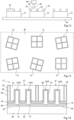
- FIG. 1 and the Figure 2 are respectively a side sectional view and a partial and schematic top view of a structure obtained at a step of an embodiment of a method for manufacturing an optoelectronic device corresponding to a display screen.
- the method comprises forming on a semiconductor wafer 10 a plurality of copies of a display pixel 12, also called a display pixel circuit, for a display screen.
- the wafer 10 may rest on a support 11.
- Each display pixel 12 comprises several display sub-pixels 14, for example three or four display sub-pixels 14.
- each display pixel 12 comprises four display sub-pixels 14.
- Each display sub-pixel 14 comprises a light source, not shown, for example a light-emitting diode.
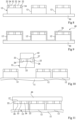
- FIG. 5 and the Figure 6 are respectively a side sectional view and a partial and schematic top view of the structure obtained after a step of placing at least a portion of the display pixels 12 on a support 30, also called a slab, of the display screen.
- the method for placing the display pixels 12 implements a pick and place method in which the display pixels 12 are manipulated individually one after the other to be placed at desired locations on the slab 30, for example using a gripper.
- the method for manipulating the display pixels 12 implements a mass transfer method in which several display pixels 12 are manipulated simultaneously.
- the manipulation of the display pixels 12 comprises the exertion of a mechanical force on the walls 22 and/or on the temporary blocks 26 of the display pixel 12.
- the presence of the temporary blocks 26 advantageously makes it possible to obtain a display pixel 12 having a flat upper face, which facilitates the use of a gripper.
- each display pixel 12 can be fixed to the panel 30 by molecular bonding or by means of a bonding material, in particular an electrically conductive epoxy glue.
- the slab 30 comprises connection tracks, not shown, the display pixels 12 being fixed to the connection tracks.
- the pitch between the display pixels 12 on the slab 30 is different from the pitch between the display pixel circuits 12 on the plate 10.
- FIG. 7 is a partial and schematic side sectional view of the structure obtained after a step of removing the temporary blocks 26 present in the cavities 24 of each display pixel 12. Removal of the temporary blocks 26 can be achieved by wet etching or dry etching.
- FIG 8 is a partial and schematic side sectional view of the structure obtained after a step of filling, for each display pixel 12, at least some cavities 24 of the display pixel 12, preferably each cavity 24 of the display pixel 12, with a final filling material.
- the final filling material may not be the same for each cavity 24.
- the final filling material corresponds for example to a photoluminescent material.
- a photoluminescent block 32 is then formed in the cavity 24.
- the final filling material may correspond for example to a non-photoluminescent and transparent material.
- a transparent block 34 is then formed in the cavity 24.
- all the temporary blocks 26 are removed at the same time and then all the photoluminescent blocks 32 and the transparent blocks 34 are formed.
- the temporary blocks 26 may not be removed all at the same time but sets of temporary blocks 26 may be removed at successive removal steps.
- a step of removing a set of temporary blocks 26 is then followed by a step of forming photoluminescent blocks 32 and/or transparent blocks 34 in at least some of the cavities 24 freed in the previous removal step.
- a removal step of another set of temporary blocks 26 followed by a step of forming photoluminescent blocks 32 and/or transparent blocks 34 in at least some of the vacated cavities 24 are then implemented, and so on.
- each photoluminescent block 32 or transparent block 34 is located opposite one of the light-emitting diodes or a set of light-emitting diodes.
- Each photoluminescent block 32 comprises phosphors or particles of at least one photoluminescent material adapted, when excited by the light emitted by the associated light-emitting diode, to emit light at a wavelength different from the wavelength of the light emitted by the associated light-emitting diode.
- the display pixel 12 comprises at least two types of photoluminescent blocks 32.
- Each photoluminescent block 32 of the first type is adapted to convert the radiation provided by the light-emitting diodes that it covers into a first radiation at a first wavelength and each photoluminescent block 32 of the second type is adapted to convert the radiation provided by the light-emitting diodes that it covers into a second radiation at a second wavelength.
- the display pixel comprises at least three types of photoluminescent blocks 32, the photoluminescent block of the third type being adapted to convert the radiation provided by the light-emitting diodes that it covers into a third radiation at a third wavelength.
- the first, second and third wavelengths may be different.
- the light-emitting diodes of the pixels 12 are adapted to emit radiation in the ultraviolet.
- the first wavelength corresponds to blue light and is in the range of 430 nm to 490 nm.
- the second wavelength corresponds to green light and is in the range of 510 nm to 570 nm.
- the third wavelength corresponds to red light and is in the range of 600 nm to 720 nm.
- each photoluminescent block 32 comprises a matrix in which nanometric-sized monocrystalline photoluminescent particles of a semiconductor material, also called semiconductor nanocrystals or nanoluminophore particles hereinafter, are dispersed.
- the internal quantum efficiency QY int of a photoluminescent material is equal to the ratio between the number of photons emitted and the number of photons absorbed by the photoluminescent substance.
- the internal quantum efficiency QY int of the semiconductor nanocrystals is greater than 5%, preferably greater than 10%, more preferably greater than 20%.
- the average size of the nanocrystals is in the range of 0.5 nm and 1000 nm, preferably from 0.5 nm to 500 nm, even more preferably from 1 nm to 100 nm, in particular from 2 nm to 30 nm.
- the photoconversion properties of the semiconductor nanocrystals depend essentially of phenomena of substantially three-dimensional quantum confinement. Semiconductor nanocrystals then correspond to quantum dots.
- the semiconductor material of the semiconductor nanocrystals is selected from the group comprising cadmium selenide (CdSe), indium phosphide (InP), cadmium sulfide (CdS), zinc sulfide (ZnS), zinc selenide (ZnSe), cadmium telluride (CdTe), zinc telluride (ZnTe), cadmium oxide (CdO), cadmium zinc oxide (ZnCdO), cadmium zinc sulfide (CdZnS), cadmium zinc selenide (CdZnSe), silver indium sulfide (AgInS 2 ), perovskites of the PbScX 3 type, where X is a halogen atom, in particular iodine (I), bromine (Br) or chlorine (Cl), and a mixture of at least two of these compounds.
- X is a halogen atom, in particular iodine (I
- the semiconductor material of the semiconductor nanocrystals is chosen from the materials cited in the publication in the name of Le Blevenec et al. by Physica Status Solidi (RRL) - Rapid Research Letters Volume 8, No. 4, pages 349-352, April 2014 .
- the dimensions of the semiconductor nanocrystals are chosen according to the desired wavelength of the radiation emitted by the semiconductor nanocrystals.
- CdSe nanocrystals whose average size is of the order of 3.6 nm are suitable for converting blue light into red light and CdSe nanocrystals whose average size is of the order of 1.3 nm are suitable for converting blue light into green light.
- the composition of the semiconductor nanocrystals is chosen according to the desired wavelength of the radiation emitted by the semiconductor nanocrystals.
- the matrix of the photoluminescent blocks 32 is transparent to the radiation emitted by the photoluminescent particles and/or the light-emitting diodes LED, preferably more than 80%.
- the matrix is, for example, made of silica.
- the matrix is, for example, made of any polymer that is at least partly transparent, in particular silicone, epoxy, acrylic resin of the poly(methyl methacrylate) (PMMA) type, or polyacetic acid (PLA).
- PMMA poly(methyl methacrylate)
- PPA polyacetic acid
- the matrix may in particular be made of an at least partly transparent polymer used with three-dimensional printers.
- the matrix may correspond to a spin-on glass (SOG), photosensitive or non-photosensitive.
- the matrix contains from 2% to 90%, preferably from 10% to 60%, by weight of nanocrystals, for example approximately 30% by weight of nanocrystals.
- the transparent blocks 34 comprise only the matrix as described above.
- the thickness of the photoluminescent blocks 32 depends on the concentration of nanocrystals and the type of nanocrystals used.
- the height of the photoluminescent blocks 32 is less than or equal to the height of the walls 22.
- each photoluminescent block 32 may correspond to a square, a rectangle, an "L" shaped polygon, etc., the area of which may be equal to the area of a square having a side measuring from 1 ⁇ m to 100 ⁇ m, preferably from 3 ⁇ m to 15 ⁇ m.
- the aspect ratio of the blocks 32 i.e. the ratio between the height and the maximum width of the block, may be between 0.01 and 10, preferably between 0.05 and 2.
- the filling of the cavities 24 with the final filling material is carried out by inkjet printing, in particular by electrodynamic jet printing, by aerosol jet printing, or by extrusion printing.
- the manipulation of the display pixels 12 comprises the exertion of a mechanical force on the walls 22 and/or on the temporary blocks 26 of the display pixel 12.
- the presence of the temporary blocks 26 advantageously makes it possible to obtain a display pixel 12 having a substantially flat upper face 27, which facilitates the use of a gripper.
- the temporary blocks 26 may not be present.
- the manipulation of the display pixels 12 may then comprise the exertion of a mechanical force only on the walls 22 of the display pixel 12.
Landscapes
- Devices For Indicating Variable Information By Combining Individual Elements (AREA)
Applications Claiming Priority (1)
| Application Number | Priority Date | Filing Date | Title |
|---|---|---|---|
| FR2315318A FR3157660A1 (fr) | 2023-12-26 | 2023-12-26 | Procédé de fabrication d'un dispositif optoélectronique |
Publications (1)
| Publication Number | Publication Date |
|---|---|
| EP4580353A1 true EP4580353A1 (de) | 2025-07-02 |
Family
ID=91248926
Family Applications (1)
| Application Number | Title | Priority Date | Filing Date |
|---|---|---|---|
| EP24222631.4A Pending EP4580353A1 (de) | 2023-12-26 | 2024-12-20 | Verfahren zur herstellung einer optoelektronischen vorrichtung und durch dieses verfahren erhaltene anzeigevorrichtung |
Country Status (3)
| Country | Link |
|---|---|
| US (1) | US12514048B2 (de) |
| EP (1) | EP4580353A1 (de) |
| FR (1) | FR3157660A1 (de) |
Citations (4)
| Publication number | Priority date | Publication date | Assignee | Title |
|---|---|---|---|---|
| US20190371779A1 (en) * | 2018-06-01 | 2019-12-05 | Samsung Electronics Co., Ltd. | Method of manufacturing display module using led |
| US20210020619A1 (en) * | 2019-07-17 | 2021-01-21 | Sharp Fukuyama Semiconductor Co., Ltd. | Micro light emitting element and image display device |
| US20210135064A1 (en) * | 2019-10-31 | 2021-05-06 | Sharp Fukuyama Semiconductor Co., Ltd. | Display device and manufacturing method of display device |
| US20210336095A1 (en) * | 2018-10-12 | 2021-10-28 | Boe Technology Group Co., Ltd. | Micro light emitting diode display panel, micro light emitting diode display apparatus, and method of fabricating micro light emitting diode display panel |
Family Cites Families (3)
| Publication number | Priority date | Publication date | Assignee | Title |
|---|---|---|---|---|
| FR3051965A1 (fr) * | 2016-05-27 | 2017-12-01 | Commissariat Energie Atomique | Procede de formation d’un motif de guidage fonctionnalise pour un procede de grapho-epitaxie |
| FR3103057B1 (fr) * | 2019-11-08 | 2021-11-19 | Aledia | Procede de protection d'un dispositif optoelectronique contre les decharges electrostatiques |
| KR102762427B1 (ko) * | 2020-06-17 | 2025-02-04 | 삼성디스플레이 주식회사 | 표시 장치 |
-
2023
- 2023-12-26 FR FR2315318A patent/FR3157660A1/fr active Pending
-
2024
- 2024-12-20 EP EP24222631.4A patent/EP4580353A1/de active Pending
- 2024-12-20 US US18/989,552 patent/US12514048B2/en active Active
Patent Citations (4)
| Publication number | Priority date | Publication date | Assignee | Title |
|---|---|---|---|---|
| US20190371779A1 (en) * | 2018-06-01 | 2019-12-05 | Samsung Electronics Co., Ltd. | Method of manufacturing display module using led |
| US20210336095A1 (en) * | 2018-10-12 | 2021-10-28 | Boe Technology Group Co., Ltd. | Micro light emitting diode display panel, micro light emitting diode display apparatus, and method of fabricating micro light emitting diode display panel |
| US20210020619A1 (en) * | 2019-07-17 | 2021-01-21 | Sharp Fukuyama Semiconductor Co., Ltd. | Micro light emitting element and image display device |
| US20210135064A1 (en) * | 2019-10-31 | 2021-05-06 | Sharp Fukuyama Semiconductor Co., Ltd. | Display device and manufacturing method of display device |
Non-Patent Citations (1)
| Title |
|---|
| LE BLEVENEC ET AL., PHYSICA STATUS SOLIDI (RRL) - RAPID RESEARCH LETTERS, vol. 8, no. 4, April 2014 (2014-04-01), pages 349 - 352 |
Also Published As
| Publication number | Publication date |
|---|---|
| US20250212580A1 (en) | 2025-06-26 |
| US12514048B2 (en) | 2025-12-30 |
| FR3157660A1 (fr) | 2025-06-27 |
Similar Documents
| Publication | Publication Date | Title |
|---|---|---|
| EP3646392B1 (de) | Optoelektronische vorrichtung | |
| EP3024030B1 (de) | Optoelektronische vorrichtung mit leuchtdioden und herstellungsverfahren dafür | |
| US11171267B2 (en) | Process for fabricating an optoelectronic device including photoluminescent pads of photoresist | |
| EP3815139B1 (de) | Optoelektronische vorrichtung mit leuchtdioden | |
| FR3061603A1 (fr) | Dispositif optoelectronique a diodes electroluminescentes | |
| EP3900039A1 (de) | Optoelektronische vorrichtung zur aufnahme von bildern mit mehreren blickpunkten und/oder zur anzeige von bildern mit mehreren blickpunkten | |
| EP4042482B1 (de) | Verfahren zur herstellung einer optoelektronischen vorrichtung | |
| EP4580353A1 (de) | Verfahren zur herstellung einer optoelektronischen vorrichtung und durch dieses verfahren erhaltene anzeigevorrichtung | |
| EP3871255B1 (de) | Optoelektronische vorrichtung mit leuchtdioden mit verbesserter lichtextraktion und ein verfahren zu seiner herstellung | |
| EP4437589B1 (de) | Leuchtdiodenanzeigepixel für einen anzeigebildschirm | |
| EP4454016A1 (de) | Anzeigeschirm mit leuchtdioden | |
| WO2024104900A1 (fr) | Puce optoélectronique émissive monolithique | |
| WO2024003085A1 (fr) | Dispositif optoélectronique et procédé de fabrication | |
| EP4576182A2 (de) | Verfahren zur herstellung einer elektronischen vorrichtung | |
| FR3103057A1 (fr) | Procede de protection d'un dispositif optoelectronique contre les decharges electrostatiques | |
| FR3144404A1 (fr) | Dispositif optoélectronique à diodes électroluminescentes tridimensionnelles | |
| WO2024141405A1 (fr) | Procédé d'ajustement de la longueur d'onde centrale d'un dispositif optoélectronique à diodes électroluminescentes tridimensionnelles | |
| FR3150042A1 (fr) | Ecran d'affichage a diodes electroluminescentes a extraction de lumiere amelioree et pixels d'affichage pour un tel ecran | |
| FR3144532A1 (fr) | Procede de fabrication d'un dispositif electronique |
Legal Events
| Date | Code | Title | Description |
|---|---|---|---|
| PUAI | Public reference made under article 153(3) epc to a published international application that has entered the european phase |
Free format text: ORIGINAL CODE: 0009012 |
|
| STAA | Information on the status of an ep patent application or granted ep patent |
Free format text: STATUS: THE APPLICATION HAS BEEN PUBLISHED |
|
| AK | Designated contracting states |
Kind code of ref document: A1 Designated state(s): AL AT BE BG CH CY CZ DE DK EE ES FI FR GB GR HR HU IE IS IT LI LT LU LV MC ME MK MT NL NO PL PT RO RS SE SI SK SM TR |
|
| STAA | Information on the status of an ep patent application or granted ep patent |
Free format text: STATUS: REQUEST FOR EXAMINATION WAS MADE |
|
| 17P | Request for examination filed |
Effective date: 20250728 |