EP4579763A1 - Cellule solaire et module photovoltaïque - Google Patents
Cellule solaire et module photovoltaïque Download PDFInfo
- Publication number
- EP4579763A1 EP4579763A1 EP24169521.2A EP24169521A EP4579763A1 EP 4579763 A1 EP4579763 A1 EP 4579763A1 EP 24169521 A EP24169521 A EP 24169521A EP 4579763 A1 EP4579763 A1 EP 4579763A1
- Authority
- EP
- European Patent Office
- Prior art keywords
- substrate
- doped
- layer
- conductive layer
- solar cell
- Prior art date
- Legal status (The legal status is an assumption and is not a legal conclusion. Google has not performed a legal analysis and makes no representation as to the accuracy of the status listed.)
- Pending
Links
Images

Classifications
-
- H—ELECTRICITY
- H10—SEMICONDUCTOR DEVICES; ELECTRIC SOLID-STATE DEVICES NOT OTHERWISE PROVIDED FOR
- H10F—INORGANIC SEMICONDUCTOR DEVICES SENSITIVE TO INFRARED RADIATION, LIGHT, ELECTROMAGNETIC RADIATION OF SHORTER WAVELENGTH OR CORPUSCULAR RADIATION
- H10F77/00—Constructional details of devices covered by this subclass
- H10F77/30—Coatings
- H10F77/306—Coatings for devices having potential barriers
- H10F77/311—Coatings for devices having potential barriers for photovoltaic cells
-
- H—ELECTRICITY
- H10—SEMICONDUCTOR DEVICES; ELECTRIC SOLID-STATE DEVICES NOT OTHERWISE PROVIDED FOR
- H10F—INORGANIC SEMICONDUCTOR DEVICES SENSITIVE TO INFRARED RADIATION, LIGHT, ELECTROMAGNETIC RADIATION OF SHORTER WAVELENGTH OR CORPUSCULAR RADIATION
- H10F77/00—Constructional details of devices covered by this subclass
- H10F77/20—Electrodes
- H10F77/206—Electrodes for devices having potential barriers
- H10F77/211—Electrodes for devices having potential barriers for photovoltaic cells
- H10F77/219—Arrangements for electrodes of back-contact photovoltaic cells
-
- H—ELECTRICITY
- H10—SEMICONDUCTOR DEVICES; ELECTRIC SOLID-STATE DEVICES NOT OTHERWISE PROVIDED FOR
- H10F—INORGANIC SEMICONDUCTOR DEVICES SENSITIVE TO INFRARED RADIATION, LIGHT, ELECTROMAGNETIC RADIATION OF SHORTER WAVELENGTH OR CORPUSCULAR RADIATION
- H10F10/00—Individual photovoltaic cells, e.g. solar cells
- H10F10/10—Individual photovoltaic cells, e.g. solar cells having potential barriers
- H10F10/14—Photovoltaic cells having only PN homojunction potential barriers
- H10F10/146—Back-junction photovoltaic cells, e.g. having interdigitated base-emitter regions on the back side
-
- H—ELECTRICITY
- H10—SEMICONDUCTOR DEVICES; ELECTRIC SOLID-STATE DEVICES NOT OTHERWISE PROVIDED FOR
- H10F—INORGANIC SEMICONDUCTOR DEVICES SENSITIVE TO INFRARED RADIATION, LIGHT, ELECTROMAGNETIC RADIATION OF SHORTER WAVELENGTH OR CORPUSCULAR RADIATION
- H10F19/00—Integrated devices, or assemblies of multiple devices, comprising at least one photovoltaic cell covered by group H10F10/00, e.g. photovoltaic modules
- H10F19/80—Encapsulations or containers for integrated devices, or assemblies of multiple devices, having photovoltaic cells
-
- H—ELECTRICITY
- H10—SEMICONDUCTOR DEVICES; ELECTRIC SOLID-STATE DEVICES NOT OTHERWISE PROVIDED FOR
- H10F—INORGANIC SEMICONDUCTOR DEVICES SENSITIVE TO INFRARED RADIATION, LIGHT, ELECTROMAGNETIC RADIATION OF SHORTER WAVELENGTH OR CORPUSCULAR RADIATION
- H10F19/00—Integrated devices, or assemblies of multiple devices, comprising at least one photovoltaic cell covered by group H10F10/00, e.g. photovoltaic modules
- H10F19/90—Structures for connecting between photovoltaic cells, e.g. interconnections or insulating spacers
- H10F19/902—Structures for connecting between photovoltaic cells, e.g. interconnections or insulating spacers for series or parallel connection of photovoltaic cells
- H10F19/908—Structures for connecting between photovoltaic cells, e.g. interconnections or insulating spacers for series or parallel connection of photovoltaic cells for back-contact photovoltaic cells
-
- H—ELECTRICITY
- H10—SEMICONDUCTOR DEVICES; ELECTRIC SOLID-STATE DEVICES NOT OTHERWISE PROVIDED FOR
- H10F—INORGANIC SEMICONDUCTOR DEVICES SENSITIVE TO INFRARED RADIATION, LIGHT, ELECTROMAGNETIC RADIATION OF SHORTER WAVELENGTH OR CORPUSCULAR RADIATION
- H10F77/00—Constructional details of devices covered by this subclass
- H10F77/10—Semiconductor bodies
- H10F77/14—Shape of semiconductor bodies; Shapes, relative sizes or dispositions of semiconductor regions within semiconductor bodies
- H10F77/147—Shapes of bodies
-
- H—ELECTRICITY
- H10—SEMICONDUCTOR DEVICES; ELECTRIC SOLID-STATE DEVICES NOT OTHERWISE PROVIDED FOR
- H10F—INORGANIC SEMICONDUCTOR DEVICES SENSITIVE TO INFRARED RADIATION, LIGHT, ELECTROMAGNETIC RADIATION OF SHORTER WAVELENGTH OR CORPUSCULAR RADIATION
- H10F77/00—Constructional details of devices covered by this subclass
- H10F77/10—Semiconductor bodies
- H10F77/14—Shape of semiconductor bodies; Shapes, relative sizes or dispositions of semiconductor regions within semiconductor bodies
- H10F77/148—Shapes of potential barriers
-
- H—ELECTRICITY
- H10—SEMICONDUCTOR DEVICES; ELECTRIC SOLID-STATE DEVICES NOT OTHERWISE PROVIDED FOR
- H10F—INORGANIC SEMICONDUCTOR DEVICES SENSITIVE TO INFRARED RADIATION, LIGHT, ELECTROMAGNETIC RADIATION OF SHORTER WAVELENGTH OR CORPUSCULAR RADIATION
- H10F77/00—Constructional details of devices covered by this subclass
- H10F77/30—Coatings
- H10F77/306—Coatings for devices having potential barriers
- H10F77/311—Coatings for devices having potential barriers for photovoltaic cells
- H10F77/315—Coatings for devices having potential barriers for photovoltaic cells the coatings being antireflective or having enhancing optical properties
-
- H—ELECTRICITY
- H10—SEMICONDUCTOR DEVICES; ELECTRIC SOLID-STATE DEVICES NOT OTHERWISE PROVIDED FOR
- H10F—INORGANIC SEMICONDUCTOR DEVICES SENSITIVE TO INFRARED RADIATION, LIGHT, ELECTROMAGNETIC RADIATION OF SHORTER WAVELENGTH OR CORPUSCULAR RADIATION
- H10F77/00—Constructional details of devices covered by this subclass
- H10F77/70—Surface textures, e.g. pyramid structures
- H10F77/707—Surface textures, e.g. pyramid structures of the substrates or of layers on substrates, e.g. textured ITO layer on a glass substrate
Definitions
- IBC Interdigitated Back Contact
- the IBC cell may also include other film layers such as a passivation antireflection layer located on a surface of the doped conductive layer away from the substrate and/or a passivation antireflection layer located on the front surface of the substrate, which are not detailed here.
- a passivation antireflection layer located on a surface of the doped conductive layer away from the substrate and/or a passivation antireflection layer located on the front surface of the substrate, which are not detailed here.
- the solar cell includes a substrate 101 having a front surface and a rear surface opposite to the front surface, and the substrate 101 is doped with a second dopant element.
- the solar cell includes a first dielectric layer 102 formed over the rear surface of the substrate 101, and a first doped conductive layer 103 formed over a surface of the first dielectric layer 102 away from the substrate 101.
- the first doped conductive layer 103 is doped with a first dopant element, one of the first dopant element and the second dopant element is a P-type dopant element and the other of the first dopant element and the second dopant element is an N-type dopant element.
- the solar cell includes multiple grooves 104 arranged at intervals in a first direction, penetrating the first doped conductive layer 103 and the first dielectric layer 102 and extending into the the substrate 101.
- the solar cell includes a second dielectric layer 105 formed over bottom surfaces of the grooves 104 and a second doped conductive layer 106 formed over a surface of the second dielectric layer 105 away from the substrate 101.
- the second doped conductive layer 106 is doped with the second dopant element.
- the solar cell includes a doped layer 107 aligned with the second doped conductive layer 106, located between the second dielectric layer 105 and the substrate 101, and doped with the first dopant element.
- the second doped conductive layer 106 is doped with the second dopant element.
- the solar cell includes a doped layer 107 having a plurality of portions, a respective portion of the doped layer 107 is aligned with the respective portion of the second doped conductive layer 106, and located on a side of the respective portion of the second dielectric layer 105 facing a bottom of the respective groove, and the doped layer 107 is doped with the first dopant element.
- the top surface of the first dielectric layer 102 facing toward the substrate 101 may be level with the bottom surface of the second doped conductive layer 106 away from the substrate 101, or the top surface of the first dielectric layer 102 facing toward the substrate 101 may be higher than the bottom surface of the second doped conductive layer 106 away from the substrate 101, as long as it is ensured that a bottom surface of the first doped conductive layer 103 facing toward the substrate 101 is farther away from the substrate than the bottom surface of the second doped conductive layer 106 away from the substrate 101, that is, the first doped conductive layer 103 is not in contact with the second doped conductive layer 106.
- the doped layer 107 and the second dielectric layer 105 may have the same length and width as the second doped conductive layer 106, or a length tolerance and a width tolerance among the doped layer 107, the second dielectric layer 105 and the second doped conductive layer 106 may be less than a preset value, for example, 2%, 5% or 10% or the like.
- the first dielectric layer 102 may have the same length and width as the first doped conductive layer 103, or a length tolerance and a width tolerance between the first dielectric layer 102 and the first doped conductive layer 103 may be less than a preset value, for example, 2%, 5% or 10% or the like.
- the solar cell is provided with a passivation contact structure formed by the first dielectric layer 102 and the first doped conductive layer 103 and a passivation contact structure formed by the second dielectric layer 105 and the second doped conductive layer 106.
- the passivation contact structure can apply good passivation to the substrate 101, so that the open-circuit voltage of the solar cell can be increased, and the carrier recombination on the rear surface of the substrate 101 can be reduced, thereby reducing the carrier recombination loss of the solar cell.
- the doped conductive layers include the first doped conductive layer 103 and the second doped conductive layer 106 with different doping types, so that all of the electrodes of the solar cell can be arranged on the rear surface of the solar cell, the light shielding effect caused by the arrangement of the electrodes on the front surface of the solar cell is avoided, and the light absorption of the solar cell is improved.
- the front surface of the solar cell refers to the surface of the solar cell which receives a greater intensity of incident light
- the rear surface of the solar cell refers to the surface of the solar cell which receives a less intensity of incident light.
- the doped layer 107 is arranged between the second dielectric layer 105 and the substrate 101 and is arranged to be aligned with the second doped conductive layer 106.
- the doped layer 107 is doped with a doping type different from the doping types of the substrate 101 and the second doped conductive layer 106.
- the electric field formed between the doped layer 107 and the substrate 101 can improve an efficiency of a specific polarity of carriers converging to a region in the substrate 101 which is aligned with the second doped conductive layer 106, thereby reducing the carrier converging loss of the solar cell.
- the electric field formed between the doped layer 107 and the second doped conductive layer 106 can improve a passivation effect of the substrate 101, increase the open-circuit voltage of the solar cell, reduce the carrier recombination loss on the rear surface of the substrate 101, and improve the photoelectric conversion efficiency of the solar cell.
- the substrate 101 may be a P-type semiconductor substrate or an N-type semiconductor substrate.
- One of the first dopant element and the second dopant element is a P-type dopant element and the other of the first dopant element and the second dopant element is an N-type dopant element.
- the second doped conductive layer 106 is doped with the same doping type as the substrate 101. Moreover, a doping concentration of the second dopant element in the second doped conductive layer 106 is higher than a doping concentration of the second dopant element in the substrate 101, where the doping concentration may be represented by an atomic percentage of the dopant element in the film layer.
- the N-type semiconductor substrate is doped with N-type dopant elements, and the N-type dopant element may be any one of group-V elements such as phosphorus (P) element, bismuth (Bi) element, antimony (Sb) element or arsenic (As) element.
- the P-type semiconductor substrate is doped with P-type dopant elements, and the P-type dopant element may be any one of group-III elements such as boron (B) element, aluminum (Al) element, gallium (Ga) element or indium (In) element.
- the substrate 101 may be made of an elemental semiconductor material consisting of a single element, such as silicon or germanium.
- the elemental semiconductor material may be of a monocrystalline state, a polycrystalline state, an amorphous state or a microcrystalline state (having both the monocrystalline state and the amorphous state).
- silicon may be at least one of monocrystalline silicon, polycrystalline silicon, amorphous silicon or microcrystalline silicon.
- the substrate 101 may be made of compound semiconductor material.
- compound semiconductor materials include, but are not limited to, silicon germanide, silicon carbide, gallium arsenide, indium gallium, perovskite, cadmium telluride, or copper indium selenium.
- the substrate 101 may also be a sapphire substrate, a silicon substrate on an insulator, or a germanium substrate on an insulator.
- the first dielectric layer 102 may be made of at least one of silicon oxide, silicon nitride, silicon oxynitride, silicon carbide or magnesium fluoride.
- the second dielectric layer 105 may be made of at least one of silicon oxide, silicon nitride, silicon oxynitride, silicon carbide or magnesium fluoride.
- the first doped conductive layer 103 may be made of at least one of nanocrystalline silicon, polycrystalline silicon, microcrystalline silicon, amorphous silicon, silicon carbide or titanium nitride or the like.
- the second doped conductive layer 106 may be made of at least one of nanocrystalline silicon, polycrystalline silicon, microcrystalline silicon, amorphous silicon, silicon carbide or titanium nitride or the like.
- the material of the doped layer 107 may be similar to the material of the substrate 101 and may be at least one of monocrystalline silicon, polycrystalline silicon, amorphous silicon or microcrystalline silicon, and may also be a compound semiconductor material.
- a ratio of a doping concentration of the first dopant element in the doped layer 107 to a doping concentration of the first dopant element in the first doped conductive layer 103 ranges from 1 ⁇ 10 -4 to 1 ⁇ 10 -3 .
- the electric field is formed between the doped layer 107 and the substrate 101 with the doping type different from the doping type of the doped layer 107, the efficiency of the specific type of carriers converging to the region in the substrate 101 which is aligned with the second doped conductive layer 106 is improved, the carrier converging loss of the region in the substrate 101 which is aligned with the second doped conductive layer 106 is reduced.
- the electric field is formed between the doped layer 107 and the second doped conductive layer 106 with the doping type different from the doping type of the doped layer 107, the passivation effect of the rear surface of the substrate 101 is improved, the open-circuit voltage of the solar cell is increased, the carrier recombination loss of the solar cell is reduced.
- an electron hole recombination effect of the carrier in the doped layer 107 may be significantly improved during the transmission of the carrier to the second doped conductive layer 106 through the doped layer 107, thus resulting in a case that the impact of the carrier recombination loss in the doped layer 107 on the photoelectric conversion efficiency of the solar cell is higher than the impact of reduction in the carrier recombination loss of the substrate 101 on the photoelectric conversion efficiency of the solar cell, therefore, the photoelectric conversion efficiency of the solar cell is reduced.
- the doping concentration of the first dopant element in the doped layer 107 may be set in a range from 1 ⁇ 10 14 /cm 3 to 9 ⁇ 10 18 /cm 3 , for example, 2 ⁇ 10 14 /cm 3 , 5 ⁇ 10 14 /cm 3 , 8 ⁇ 10 14 /cm 3 , 1.25 ⁇ 10 15 /cm 3 , 2.5 ⁇ 10 15 /cm 3 , 5 ⁇ 10 15 /cm 3 , 1 ⁇ 10 16 /cm 3 , 2.5 ⁇ 10 16 /cm 3 , 5 ⁇ 10 16 /cm 3 , 1 ⁇ 10 17 /cm 3 , 2 ⁇ 10 17 /cm 3 , 3.5 ⁇ 10 17 /cm 3 , 5 ⁇ 10 17 /cm 3 , 1 ⁇ 10 18 /cm 3 , 4 ⁇ 10 18 /cm 3 , 8 ⁇ 10 18 /cm 3 , or the like.
- the second dielectric layer 105 is directly formed on the bottom surface of the grooves 104 by the selective deposition process, and the second doped conductive layer 106 is formed on the surface of the second dielectric layer 105 away from the substrate 101 by the selective deposition process and the doping process.
- the antireflection layer 310 may be made of at least one of silicon oxide, aluminium oxide, silicon nitride or silicon oxynitride.
- the antireflection layer 310 has a single layer structure or a multiple-layer structure.
- the layers are sequentially stacked in a direction perpendicular to the front surface of the substrate 301, the materials of different layers may be different, or the materials of some layers may be the same and different from the materials of other layers.
- the multiple-layer structure may be a double-layer structure including a silicon nitride layer and a silicon oxynitride layer which are stacked.
- the substrate 301, the first dielectric layer 302, the first doped conductive layer 303, the grooves 304, the second dielectric layer 305, the second doped conductive layer 306 and the doped layer 307 are respectively similar to the substrate 101, the first dielectric layer 102, the first doped conductive layer 103, the grooves 104, the second dielectric layer 105, the second doped conductive layer 106 and the doped layer 107 mentioned above, and description for them are not repeated here.
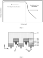
- FIG. 7 is a schematic diagram of an overall structure of a solar cell, where the X direction represents the first direction.
- a surface of the antireflection layer 310 away from the substrate 301 is a textured surface.
- the surface of the antireflection layer 310 away from the substrate 301 may be arranged as a textured surface.
- an initial antireflection layer with a surface away from the substrate 301 being a smooth surface, is firstly formed on the surface of the substrate 301, then the surface of the initial antireflection layer away from the substrate 301 is processed by the patterning or texturing process, to form the antireflection layer 310.
- the surface of the antireflection layer 310 away from the substrate 301 has multiple convex structures, so that the surface of the antireflection layer 310 away from the substrate 301 is a textured surface.
- the smooth surface refers to a surface with a surface roughness lower than a preset value, for example, the surface roughness is less than 50nm or 200nm.
- the convex structure may be a pyramid structure, a pyramid-like structure or other pyramidal structures.
- the surface of the antireflection layer 310 away from the substrate 301 has multiple convex structures, the textured surface formed by the convex structures can further reduce the reflection of the antireflection layer 310 on the incident light, and further improve the light absorption of the solar cell.
- a surface of the antireflection layer 310 in contact with the substrate 301 is a textured surface.
- the surface of the antireflection layer 310 facing towards the substrate 301 may also be arranged as a textured surface containing multiple convex structures.
- the substrate 301 and the antireflection layer 310 can effectively improve the optical path of the incident light in the solar cell and improve the light absorption of the solar cell, so as to improve the photoelectric conversion efficiency of the solar cell.
- the convex structure may be a pyramid structure, a pyramid-like structure or other pyramidal structures.
- the substrate is provided with a passivation contact structure formed by the first dielectric layer and the first doped conductive layer and a passivation contact structure formed by the second dielectric layer and the second doped conductive layer, so as to significantly reduce carrier recombination on the rear surface of the substrate, thus reducing a recombination current on the rear surface of the substrate. In this way, carrier recombination loss of the solar cell is reduced.
- the doped conductive layers include the first doped conductive layer and the second doped conductive layer with different doping types, so that all of the electrodes of the solar cell can be arranged on the rear surface of the solar cell, the influence of the electrodes, located on the front surface of the solar cell, on the light absorption of the cell are significantly reduced, and the light absorption of the solar cell is improved.
- the doped layer, with the doping type different from the doping types of the substrate and the second doped conductive layer, is arranged between the substrate and the second dielectric layer.
- An electric field is formed between the substrate and the doped layer and an electric field is formed between the doped layer and the second doped conductive layer, thereby improving an efficiency of a specific type of carriers in the substrate converging to a region aligned with the second doped conductive layer.
- a passivation effect of the substrate is improved and the open-circuit voltage of the solar cell is increased, the carrier recombination on the rear surface of the substrate is reduced, and the photoelectric conversion efficiency of the solar cell is significantly improved.
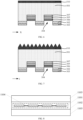
- the photovoltaic module includes at least one cell string 1101 formed by connecting multiple solar cells described above or multiple cells prepared by the method described above; at least one encapsulation layer 1102 configured to cover surfaces of the at least one cell string 1101; and at least one cover plate 1103 configured to cover surfaces of the at least one encapsulation layer 1102 away from the at least one cell string 1101.
- the multiple solar cells are electrically connected in whole or in pieces to form multiple cell strings 1101 electrically connected in series and/or in parallel.
- the multiple cell strings 1101 may be electrically connected to each other by conductive strips 1104.
- the at least one encapsulation layer 1102 covers the front surface and the rear surface of the solar cell.
- the at least one encapsulation layer 1102 may be an organic encapsulation adhesive film such as an ethylenevinyl acetate copolymer (EVA) adhesive film, a polyethylene octene co-elastomer (POE) adhesive film, a polyethylene terephthalate (PET) adhesive film.
- EVA ethylenevinyl acetate copolymer
- POE polyethylene octene co-elastomer
- PET polyethylene terephthalate
- the at least one cover plate 1103 may be a glass cover plate, a plastic cover plate, or the like having a light transmitting function.
- the surface of the at least one cover plate 1103 facing towards the at least one encapsulation layer 1102 may be a textured surface, thereby increasing utilization of the incident light.
Landscapes
- Photovoltaic Devices (AREA)
Applications Claiming Priority (1)
| Application Number | Priority Date | Filing Date | Title |
|---|---|---|---|
| CN202311848785.3A CN117690983A (zh) | 2023-12-28 | 2023-12-28 | 太阳能电池及光伏组件 |
Publications (1)
| Publication Number | Publication Date |
|---|---|
| EP4579763A1 true EP4579763A1 (fr) | 2025-07-02 |
Family
ID=90135326
Family Applications (1)
| Application Number | Title | Priority Date | Filing Date |
|---|---|---|---|
| EP24169521.2A Pending EP4579763A1 (fr) | 2023-12-28 | 2024-04-10 | Cellule solaire et module photovoltaïque |
Country Status (3)
| Country | Link |
|---|---|
| US (1) | US12593528B2 (fr) |
| EP (1) | EP4579763A1 (fr) |
| CN (1) | CN117690983A (fr) |
Families Citing this family (1)
| Publication number | Priority date | Publication date | Assignee | Title |
|---|---|---|---|---|
| CN119744025A (zh) * | 2024-05-24 | 2025-04-01 | 隆基绿能科技股份有限公司 | 光伏组件、太阳能电池及其制备方法 |
Citations (7)
| Publication number | Priority date | Publication date | Assignee | Title |
|---|---|---|---|---|
| KR20110020659A (ko) * | 2009-08-24 | 2011-03-03 | 주식회사 효성 | 개선된 후면구조를 구비한 후면접합 태양전지 및 그 제조방법 |
| US20140020752A1 (en) * | 2011-03-25 | 2014-01-23 | Sanyo Electric Co., Ltd. | Photoelectric converter, and method for producing same |
| AU2017221854A1 (en) * | 2011-12-21 | 2017-09-21 | Sunpower Corporation | Hybrid polysilicon heterojunction back contact cell |
| US20170288074A1 (en) * | 2016-04-01 | 2017-10-05 | David D. Smith | Metallization of solar cells with differentiated p-type and n-type region architectures |
| US20210175374A1 (en) * | 2019-12-10 | 2021-06-10 | Sunpower Corporation | Aligned metallization for solar cells |
| US20220393052A1 (en) * | 2021-06-04 | 2022-12-08 | Solarlab Aiko Europe Gmbh | Back contact structure and selective contact region buried solar cell comprising the same |
| US20230369530A1 (en) * | 2020-10-09 | 2023-11-16 | International Solar Energy Research Center Konstanz E.V. | Method for local modification of etching resistance in a silicon layer, use of this method in the productions of passivating contact solar cells and thus-created solar cell |
Family Cites Families (13)
| Publication number | Priority date | Publication date | Assignee | Title |
|---|---|---|---|---|
| DE102007059490B4 (de) * | 2007-12-11 | 2012-10-25 | Institut Für Solarenergieforschung Gmbh | Rückkontaktsolarzelle mit integrierter Bypassdioden-Funktion sowie Herstellungsverfahren hierfür |
| WO2011105554A1 (fr) | 2010-02-26 | 2011-09-01 | 三洋電機株式会社 | Cellule solaire et procédé de fabrication de cellule solaire |
| WO2013040785A1 (fr) | 2011-09-23 | 2013-03-28 | 上海凯世通半导体有限公司 | Procédé de dopage, structure pn, procédé de fabrication de cellule solaire et cellule solaire |
| KR101826912B1 (ko) | 2011-11-07 | 2018-02-08 | 인텔렉츄얼 키스톤 테크놀로지 엘엘씨 | 광전변환소자 및 그 제조 방법 |
| JP6033624B2 (ja) | 2012-09-25 | 2016-11-30 | シャープ株式会社 | 光電変換素子 |
| KR102257808B1 (ko) * | 2014-01-20 | 2021-05-28 | 엘지전자 주식회사 | 태양 전지 모듈 |
| US9525083B2 (en) | 2015-03-27 | 2016-12-20 | Sunpower Corporation | Solar cell emitter region fabrication with differentiated P-type and N-type architectures and incorporating a multi-purpose passivation and contact layer |
| US20190207041A1 (en) | 2017-12-29 | 2019-07-04 | Sunpower Corporation | Solar cells having differentiated p-type and n-type architectures fabricated using an etch paste |
| WO2019181835A1 (fr) | 2018-03-23 | 2019-09-26 | 株式会社カネカ | Cellule solaire et dispositif électronique comprenant une cellule solaire |
| CN109545901A (zh) | 2018-11-28 | 2019-03-29 | 国家电投集团西安太阳能电力有限公司 | Ibc电池的制作方法 |
| CN210778636U (zh) | 2019-11-28 | 2020-06-16 | 泰州中来光电科技有限公司 | 具有多种隧道结结构的背接触太阳能电池 |
| CN111952408A (zh) | 2020-06-29 | 2020-11-17 | 泰州中来光电科技有限公司 | 一种钝化金属接触的背结太阳能电池及其制备方法 |
| US12211950B2 (en) * | 2021-07-22 | 2025-01-28 | Solarlab Aiko Europe Gmbh | Passivated contact structure and solar cell comprising the same, cell assembly, and photovoltaic system |
-
2023
- 2023-12-28 CN CN202311848785.3A patent/CN117690983A/zh active Pending
-
2024
- 2024-04-10 EP EP24169521.2A patent/EP4579763A1/fr active Pending
- 2024-04-10 US US18/632,192 patent/US12593528B2/en active Active
Patent Citations (7)
| Publication number | Priority date | Publication date | Assignee | Title |
|---|---|---|---|---|
| KR20110020659A (ko) * | 2009-08-24 | 2011-03-03 | 주식회사 효성 | 개선된 후면구조를 구비한 후면접합 태양전지 및 그 제조방법 |
| US20140020752A1 (en) * | 2011-03-25 | 2014-01-23 | Sanyo Electric Co., Ltd. | Photoelectric converter, and method for producing same |
| AU2017221854A1 (en) * | 2011-12-21 | 2017-09-21 | Sunpower Corporation | Hybrid polysilicon heterojunction back contact cell |
| US20170288074A1 (en) * | 2016-04-01 | 2017-10-05 | David D. Smith | Metallization of solar cells with differentiated p-type and n-type region architectures |
| US20210175374A1 (en) * | 2019-12-10 | 2021-06-10 | Sunpower Corporation | Aligned metallization for solar cells |
| US20230369530A1 (en) * | 2020-10-09 | 2023-11-16 | International Solar Energy Research Center Konstanz E.V. | Method for local modification of etching resistance in a silicon layer, use of this method in the productions of passivating contact solar cells and thus-created solar cell |
| US20220393052A1 (en) * | 2021-06-04 | 2022-12-08 | Solarlab Aiko Europe Gmbh | Back contact structure and selective contact region buried solar cell comprising the same |
Also Published As
| Publication number | Publication date |
|---|---|
| CN117690983A (zh) | 2024-03-12 |
| US20250221088A1 (en) | 2025-07-03 |
| US12593528B2 (en) | 2026-03-31 |
Similar Documents
| Publication | Publication Date | Title |
|---|---|---|
| US12191409B2 (en) | Solar cell and photovoltaic module | |
| EP4290587A1 (fr) | Cellule solaire et module photovoltaïque | |
| KR101867855B1 (ko) | 태양 전지 | |
| EP4571845A1 (fr) | Cellule solaire, son procédé de préparation et module photovoltaïque | |
| KR101569417B1 (ko) | 태양 전지 | |
| CN220543926U (zh) | 太阳能电池和光伏组件 | |
| US12527111B2 (en) | Solar cell and photovoltaic module | |
| EP4629783B1 (fr) | Cellule solaire, cellule solaire tandem et module photovoltaïque | |
| JP7814575B2 (ja) | 太陽電池及び光起電力モジュール | |
| CN103178132B (zh) | 太阳能电池 | |
| CN117317041A (zh) | 太阳能电池及光伏组件 | |
| EP4528826B1 (fr) | Cellule solaire et module photovoltaïque | |
| US20260059867A1 (en) | Solar cell, method for manufacturing solar cell, and photovoltaic module | |
| EP4579763A1 (fr) | Cellule solaire et module photovoltaïque | |
| JP7248856B1 (ja) | 太陽電池および太陽電池の製造方法、光起電力モジュール | |
| CN116913989A (zh) | 太阳能电池及光伏组件 | |
| US20250221085A1 (en) | Solar cell and photovoltaic module | |
| KR20160041876A (ko) | 태양 전지 |
Legal Events
| Date | Code | Title | Description |
|---|---|---|---|
| PUAI | Public reference made under article 153(3) epc to a published international application that has entered the european phase |
Free format text: ORIGINAL CODE: 0009012 |
|
| STAA | Information on the status of an ep patent application or granted ep patent |
Free format text: STATUS: REQUEST FOR EXAMINATION WAS MADE |
|
| 17P | Request for examination filed |
Effective date: 20240410 |
|
| AK | Designated contracting states |
Kind code of ref document: A1 Designated state(s): AL AT BE BG CH CY CZ DE DK EE ES FI FR GB GR HR HU IE IS IT LI LT LU LV MC ME MK MT NL NO PL PT RO RS SE SI SK SM TR |
|
| REG | Reference to a national code |
Ref country code: DE Ref legal event code: R079 Free format text: PREVIOUS MAIN CLASS: H01L0031035200 Ipc: H10F0077140000 |
|
| GRAP | Despatch of communication of intention to grant a patent |
Free format text: ORIGINAL CODE: EPIDOSNIGR1 |
|
| STAA | Information on the status of an ep patent application or granted ep patent |
Free format text: STATUS: GRANT OF PATENT IS INTENDED |
|
| RIC1 | Information provided on ipc code assigned before grant |
Ipc: H10F 77/14 20250101AFI20260310BHEP |
|
| INTG | Intention to grant announced |
Effective date: 20260318 |
|
| RIN1 | Information on inventor provided before grant (corrected) |
Inventor name: LI, HUIMIN Inventor name: XU, MENGLEI Inventor name: YANG, JIE Inventor name: ZHANG, XINYU |