EP4583383A1 - Kreisstromunterdrückungsverfahren und schaltersteuerungsvorrichtung - Google Patents
Kreisstromunterdrückungsverfahren und schaltersteuerungsvorrichtung Download PDFInfo
- Publication number
- EP4583383A1 EP4583383A1 EP24215736.0A EP24215736A EP4583383A1 EP 4583383 A1 EP4583383 A1 EP 4583383A1 EP 24215736 A EP24215736 A EP 24215736A EP 4583383 A1 EP4583383 A1 EP 4583383A1
- Authority
- EP
- European Patent Office
- Prior art keywords
- current
- voltage
- ref
- bus
- total
- Prior art date
- Legal status (The legal status is an assumption and is not a legal conclusion. Google has not performed a legal analysis and makes no representation as to the accuracy of the status listed.)
- Pending
Links
Images






Classifications
-
- H—ELECTRICITY
- H02—GENERATION; CONVERSION OR DISTRIBUTION OF ELECTRIC POWER
- H02M—APPARATUS FOR CONVERSION BETWEEN AC AND AC, BETWEEN AC AND DC, OR BETWEEN DC AND DC, AND FOR USE WITH MAINS OR SIMILAR POWER SUPPLY SYSTEMS; CONVERSION OF DC OR AC INPUT POWER INTO SURGE OUTPUT POWER; CONTROL OR REGULATION THEREOF
- H02M1/00—Details of apparatus for conversion
- H02M1/12—Arrangements for reducing harmonics from AC input or output
-
- H—ELECTRICITY
- H02—GENERATION; CONVERSION OR DISTRIBUTION OF ELECTRIC POWER
- H02M—APPARATUS FOR CONVERSION BETWEEN AC AND AC, BETWEEN AC AND DC, OR BETWEEN DC AND DC, AND FOR USE WITH MAINS OR SIMILAR POWER SUPPLY SYSTEMS; CONVERSION OF DC OR AC INPUT POWER INTO SURGE OUTPUT POWER; CONTROL OR REGULATION THEREOF
- H02M1/00—Details of apparatus for conversion
- H02M1/32—Means for protecting converters other than automatic disconnection
-
- H—ELECTRICITY
- H02—GENERATION; CONVERSION OR DISTRIBUTION OF ELECTRIC POWER
- H02M—APPARATUS FOR CONVERSION BETWEEN AC AND AC, BETWEEN AC AND DC, OR BETWEEN DC AND DC, AND FOR USE WITH MAINS OR SIMILAR POWER SUPPLY SYSTEMS; CONVERSION OF DC OR AC INPUT POWER INTO SURGE OUTPUT POWER; CONTROL OR REGULATION THEREOF
- H02M1/00—Details of apparatus for conversion
- H02M1/0003—Details of control, feedback or regulation circuits
- H02M1/0016—Control circuits providing compensation of output voltage deviations using feedforward of disturbance parameters
-
- H—ELECTRICITY
- H02—GENERATION; CONVERSION OR DISTRIBUTION OF ELECTRIC POWER
- H02M—APPARATUS FOR CONVERSION BETWEEN AC AND AC, BETWEEN AC AND DC, OR BETWEEN DC AND DC, AND FOR USE WITH MAINS OR SIMILAR POWER SUPPLY SYSTEMS; CONVERSION OF DC OR AC INPUT POWER INTO SURGE OUTPUT POWER; CONTROL OR REGULATION THEREOF
- H02M1/00—Details of apparatus for conversion
- H02M1/0003—Details of control, feedback or regulation circuits
- H02M1/0025—Arrangements for modifying reference values, feedback values or error values in the control loop of a converter
-
- H—ELECTRICITY
- H02—GENERATION; CONVERSION OR DISTRIBUTION OF ELECTRIC POWER
- H02M—APPARATUS FOR CONVERSION BETWEEN AC AND AC, BETWEEN AC AND DC, OR BETWEEN DC AND DC, AND FOR USE WITH MAINS OR SIMILAR POWER SUPPLY SYSTEMS; CONVERSION OF DC OR AC INPUT POWER INTO SURGE OUTPUT POWER; CONTROL OR REGULATION THEREOF
- H02M1/00—Details of apparatus for conversion
- H02M1/0067—Converter structures employing plural converter units, other than for parallel operation of the units on a single load
- H02M1/007—Plural converter units in cascade
-
- H—ELECTRICITY
- H02—GENERATION; CONVERSION OR DISTRIBUTION OF ELECTRIC POWER
- H02M—APPARATUS FOR CONVERSION BETWEEN AC AND AC, BETWEEN AC AND DC, OR BETWEEN DC AND DC, AND FOR USE WITH MAINS OR SIMILAR POWER SUPPLY SYSTEMS; CONVERSION OF DC OR AC INPUT POWER INTO SURGE OUTPUT POWER; CONTROL OR REGULATION THEREOF
- H02M1/00—Details of apparatus for conversion
- H02M1/12—Arrangements for reducing harmonics from AC input or output
- H02M1/123—Suppression of common mode voltage or current
-
- H—ELECTRICITY
- H02—GENERATION; CONVERSION OR DISTRIBUTION OF ELECTRIC POWER
- H02M—APPARATUS FOR CONVERSION BETWEEN AC AND AC, BETWEEN AC AND DC, OR BETWEEN DC AND DC, AND FOR USE WITH MAINS OR SIMILAR POWER SUPPLY SYSTEMS; CONVERSION OF DC OR AC INPUT POWER INTO SURGE OUTPUT POWER; CONTROL OR REGULATION THEREOF
- H02M1/00—Details of apparatus for conversion
- H02M1/42—Circuits or arrangements for compensating for or adjusting power factor in converters or inverters
- H02M1/4208—Arrangements for improving power factor of AC input
- H02M1/4216—Arrangements for improving power factor of AC input operating from a three-phase input voltage
-
- H—ELECTRICITY
- H02—GENERATION; CONVERSION OR DISTRIBUTION OF ELECTRIC POWER
- H02M—APPARATUS FOR CONVERSION BETWEEN AC AND AC, BETWEEN AC AND DC, OR BETWEEN DC AND DC, AND FOR USE WITH MAINS OR SIMILAR POWER SUPPLY SYSTEMS; CONVERSION OF DC OR AC INPUT POWER INTO SURGE OUTPUT POWER; CONTROL OR REGULATION THEREOF
- H02M1/00—Details of apparatus for conversion
- H02M1/42—Circuits or arrangements for compensating for or adjusting power factor in converters or inverters
- H02M1/4208—Arrangements for improving power factor of AC input
- H02M1/4233—Arrangements for improving power factor of AC input using a bridge converter comprising active switches
-
- H—ELECTRICITY
- H02—GENERATION; CONVERSION OR DISTRIBUTION OF ELECTRIC POWER
- H02M—APPARATUS FOR CONVERSION BETWEEN AC AND AC, BETWEEN AC AND DC, OR BETWEEN DC AND DC, AND FOR USE WITH MAINS OR SIMILAR POWER SUPPLY SYSTEMS; CONVERSION OF DC OR AC INPUT POWER INTO SURGE OUTPUT POWER; CONTROL OR REGULATION THEREOF
- H02M7/00—Conversion of AC power input into DC power output; Conversion of DC power input into AC power output
- H02M7/02—Conversion of AC power input into DC power output without possibility of reversal
- H02M7/04—Conversion of AC power input into DC power output without possibility of reversal by static converters
- H02M7/12—Conversion of AC power input into DC power output without possibility of reversal by static converters using discharge tubes with control electrode or semiconductor devices with control electrode
- H02M7/21—Conversion of AC power input into DC power output without possibility of reversal by static converters using discharge tubes with control electrode or semiconductor devices with control electrode using devices of a triode or transistor type requiring continuous application of a control signal
- H02M7/217—Conversion of AC power input into DC power output without possibility of reversal by static converters using discharge tubes with control electrode or semiconductor devices with control electrode using devices of a triode or transistor type requiring continuous application of a control signal using semiconductor devices only
-
- H—ELECTRICITY
- H02—GENERATION; CONVERSION OR DISTRIBUTION OF ELECTRIC POWER
- H02M—APPARATUS FOR CONVERSION BETWEEN AC AND AC, BETWEEN AC AND DC, OR BETWEEN DC AND DC, AND FOR USE WITH MAINS OR SIMILAR POWER SUPPLY SYSTEMS; CONVERSION OF DC OR AC INPUT POWER INTO SURGE OUTPUT POWER; CONTROL OR REGULATION THEREOF
- H02M7/00—Conversion of AC power input into DC power output; Conversion of DC power input into AC power output
- H02M7/02—Conversion of AC power input into DC power output without possibility of reversal
- H02M7/04—Conversion of AC power input into DC power output without possibility of reversal by static converters
- H02M7/12—Conversion of AC power input into DC power output without possibility of reversal by static converters using discharge tubes with control electrode or semiconductor devices with control electrode
- H02M7/21—Conversion of AC power input into DC power output without possibility of reversal by static converters using discharge tubes with control electrode or semiconductor devices with control electrode using devices of a triode or transistor type requiring continuous application of a control signal
- H02M7/217—Conversion of AC power input into DC power output without possibility of reversal by static converters using discharge tubes with control electrode or semiconductor devices with control electrode using devices of a triode or transistor type requiring continuous application of a control signal using semiconductor devices only
- H02M7/219—Conversion of AC power input into DC power output without possibility of reversal by static converters using discharge tubes with control electrode or semiconductor devices with control electrode using devices of a triode or transistor type requiring continuous application of a control signal using semiconductor devices only in a bridge configuration
-
- H—ELECTRICITY
- H02—GENERATION; CONVERSION OR DISTRIBUTION OF ELECTRIC POWER
- H02M—APPARATUS FOR CONVERSION BETWEEN AC AND AC, BETWEEN AC AND DC, OR BETWEEN DC AND DC, AND FOR USE WITH MAINS OR SIMILAR POWER SUPPLY SYSTEMS; CONVERSION OF DC OR AC INPUT POWER INTO SURGE OUTPUT POWER; CONTROL OR REGULATION THEREOF
- H02M7/00—Conversion of AC power input into DC power output; Conversion of DC power input into AC power output
- H02M7/02—Conversion of AC power input into DC power output without possibility of reversal
- H02M7/04—Conversion of AC power input into DC power output without possibility of reversal by static converters
- H02M7/12—Conversion of AC power input into DC power output without possibility of reversal by static converters using discharge tubes with control electrode or semiconductor devices with control electrode
- H02M7/21—Conversion of AC power input into DC power output without possibility of reversal by static converters using discharge tubes with control electrode or semiconductor devices with control electrode using devices of a triode or transistor type requiring continuous application of a control signal
- H02M7/217—Conversion of AC power input into DC power output without possibility of reversal by static converters using discharge tubes with control electrode or semiconductor devices with control electrode using devices of a triode or transistor type requiring continuous application of a control signal using semiconductor devices only
- H02M7/23—Conversion of AC power input into DC power output without possibility of reversal by static converters using discharge tubes with control electrode or semiconductor devices with control electrode using devices of a triode or transistor type requiring continuous application of a control signal using semiconductor devices only arranged for operation in parallel
-
- H—ELECTRICITY
- H02—GENERATION; CONVERSION OR DISTRIBUTION OF ELECTRIC POWER
- H02M—APPARATUS FOR CONVERSION BETWEEN AC AND AC, BETWEEN AC AND DC, OR BETWEEN DC AND DC, AND FOR USE WITH MAINS OR SIMILAR POWER SUPPLY SYSTEMS; CONVERSION OF DC OR AC INPUT POWER INTO SURGE OUTPUT POWER; CONTROL OR REGULATION THEREOF
- H02M7/00—Conversion of AC power input into DC power output; Conversion of DC power input into AC power output
- H02M7/42—Conversion of DC power input into AC power output without possibility of reversal
- H02M7/44—Conversion of DC power input into AC power output without possibility of reversal by static converters
- H02M7/48—Conversion of DC power input into AC power output without possibility of reversal by static converters using discharge tubes with control electrode or semiconductor devices with control electrode
- H02M7/483—Converters with outputs that each can have more than two voltages levels
- H02M7/4833—Capacitor voltage balancing
-
- H—ELECTRICITY
- H02—GENERATION; CONVERSION OR DISTRIBUTION OF ELECTRIC POWER
- H02M—APPARATUS FOR CONVERSION BETWEEN AC AND AC, BETWEEN AC AND DC, OR BETWEEN DC AND DC, AND FOR USE WITH MAINS OR SIMILAR POWER SUPPLY SYSTEMS; CONVERSION OF DC OR AC INPUT POWER INTO SURGE OUTPUT POWER; CONTROL OR REGULATION THEREOF
- H02M7/00—Conversion of AC power input into DC power output; Conversion of DC power input into AC power output
- H02M7/42—Conversion of DC power input into AC power output without possibility of reversal
- H02M7/44—Conversion of DC power input into AC power output without possibility of reversal by static converters
- H02M7/48—Conversion of DC power input into AC power output without possibility of reversal by static converters using discharge tubes with control electrode or semiconductor devices with control electrode
- H02M7/483—Converters with outputs that each can have more than two voltages levels
- H02M7/487—Neutral point clamped inverters
-
- Y—GENERAL TAGGING OF NEW TECHNOLOGICAL DEVELOPMENTS; GENERAL TAGGING OF CROSS-SECTIONAL TECHNOLOGIES SPANNING OVER SEVERAL SECTIONS OF THE IPC; TECHNICAL SUBJECTS COVERED BY FORMER USPC CROSS-REFERENCE ART COLLECTIONS [XRACs] AND DIGESTS
- Y02—TECHNOLOGIES OR APPLICATIONS FOR MITIGATION OR ADAPTATION AGAINST CLIMATE CHANGE
- Y02B—CLIMATE CHANGE MITIGATION TECHNOLOGIES RELATED TO BUILDINGS, e.g. HOUSING, HOUSE APPLIANCES OR RELATED END-USER APPLICATIONS
- Y02B70/00—Technologies for an efficient end-user side electric power management and consumption
- Y02B70/10—Technologies improving the efficiency by using switched-mode power supplies [SMPS], i.e. efficient power electronics conversion e.g. power factor correction or reduction of losses in power supplies or efficient standby modes
Definitions
- the present disclosure relates to the technical field of power conversion, specifically to a circular current suppression method, a switch control device, and a power conversion system for a parallel module configuration.
- module volume is an important factor when modules are integrated.
- one approach is to omit several switches between a negative output terminal of a module and a negative terminal of a DC bus to directly connect a negative electrode of a DC-output terminal of each module to the negative terminal of the DC bus.
- An object of the present disclosure is to provide a circular current suppression method and a switch control device to suppress circular current effectively in a configuration of parallel power conversion modules.
- One aspect of the present disclosure provides a circular current suppression method applied to a plurality of power conversion modules connected in parallel, each power conversion module including a power factor corrector, a positive bus capacitor, and a negative bus capacitor, the power factor corrector adjusting at least one of a positive bus voltage and a negative bus voltage based on at least one switching command, wherein the method includes: calculating a common-mode current based on a plurality of input currents of the power factor corrector to convert into a first reference voltage; calculating a difference between the first reference voltage and a bus-voltage difference to convert into a first reference current, wherein the bus-voltage difference is a difference between the positive bus voltage and the negative bus voltage; calculating a difference between a second reference voltage and a total voltage to convert into a total DC current, wherein the total voltage is a sum of the positive bus voltage and the negative bus voltage; adding a plurality of cosine even-numbered-harmonic components of the first reference current based on the total DC current, a target current, and one
- a switch control device including a circular-current suppression module, a voltage balance module, and a switch control module.
- the circular-current suppression module is configured to calculate a common-mode current based on a plurality of input currents of a power factor corrector to convert into a first reference voltage.
- the voltage balance module is connected to the circular-current suppression module, wherein the voltage balance module is configured to calculate a difference between the first reference voltage and a bus-voltage difference to convert into a first reference current, wherein the bus-voltage difference is a difference between the positive bus voltage and the negative bus voltage.
- the switch control module is connected to the voltage balance module and includes a total DC voltage module and at least one current control module.
- the total DC voltage module is configured to calculate a difference between a second reference voltage and a total voltage to convert into a total DC current, wherein the total voltage is a sum of the positive bus voltage and the negative bus voltage.
- the at least one current control module is connected to the total DC voltage module and configured to add a plurality of cosine even-numbered-harmonic components of the first reference current based on the total DC current, a target current, and one of the plurality of input currents to calculate a compensation current in a harmonic-current control mode and convert the compensation current into a compensation voltage to serve as one of at least one switching command.
- One aspect of the present disclosure provides a power conversion system that includes: a power source; a load; a plurality of power conversion modules connected in parallel, wherein each of the power conversion modules is configured to convert an AC power of the power source into a DC power to be provided to the load; and a plurality of switch control devices respectively connected to the plurality of power conversion modules, wherein the plurality of switch control devices are configured to execute the circular current suppression method mentioned as above.
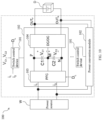
- FIG. 1 is a schematic diagram of a three-phase power conversion system 10 with a multi-module parallel topology according to a first embodiment of the present disclosure.
- the three-phase power conversion system 10 is configured to convert three-phase alternating current (AC) input power into direct current (DC) output power and adopts a multi-module parallel topology to increase the power conversion capacity of the system.
- AC alternating current
- DC direct current
- a negative output terminal OUT N of each module is directly connected to a negative terminal N of a DC bus, when a negative bus voltage V bus,N of each of modules is different, DC circular current will be generated.
- the three-phase power conversion system 10 includes a power source W, a plurality of switch control devices 11, a plurality of power conversion modules 12, and a load D, wherein the numbers of the switch control devices 11 and the power conversion modules 12 are the same.
- the power source W is a three-phase AC power source (such as R-phase, S-phase, and T-phase AC electric power)
- the load D is, for example, a DC battery or a DC load (such as a motor).
- the plurality of power conversion modules 12 are connected in parallel, and each of the power conversion modules 12 is configured to convert three-phase AC power into DC power.
- the plurality of switch control devices 11 are connected to the plurality of power conversion modules 12, respectively.
- Each switch control device 11 is configured to generate a plurality of switching commands D LR , D LS , and D LT according to input currents i LR , i LS , and i LT , a positive bus voltage V bus,P , and a negative bus voltage V bus,N .
- i LR,total i LR ,1 + ⁇ + i LR ,k ;
- i LS ,total i LS ,1 + ⁇ + i LS ,k ;
- i LT ,total i LT ,1 + ⁇ + i LT ,k , wherein k is a natural number.
- Each power conversion module 12 includes a power factor corrector (PFC) 13, a positive bus capacitor C bus,P , a negative bus capacitor C bus,N , and a direct current converter (DC/DC) 14.
- the power factor corrector 13 is connected to the power source W and is configured to convert the input currents i LR , i LS , and i LT into a positive bus voltage V bus,P and a negative bus voltage V bus,N according to a plurality of switching commands D LR , D LS , and D LT .
- the power factor corrector 13 and the DC converter 14 are connected via three buses, wherein the three buses correspond to a positive terminal P, a neutral terminal M, and a negative terminal N, respectively.
- the DC converter 14 may be, for example, the form of forward (e.g., energy is transferred directly through the magnetic field), flyback (e.g., energy is stored in the magnetic field), transformerless (non-isolated), or having a transformer (isolated), such as buck, boost, buck-boost, boost-buck, SEPIC, or CUK DC converters, but are not limited to the description here.
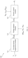
- the circular-current suppression module 21 first calculates circular current corresponding to the input currents i LR , i LS , and i LT and converts it into the first reference voltage V m,ref .
- the voltage balance module 22 calculates a difference between the first reference voltage V m,ref and the bus-voltage difference ⁇ V bus and converts it into the first reference current i m,ref .
- the switch control module 23 generates the plurality of switching commands D LR , D LS , and D LT to the power factor corrector 13 according to the first reference current i m,ref , the second reference voltage V ref , the target current i target , the target voltage V target , and the total voltage V total .
- the switching control device 11 can converge the circular current to the target current i target and converge the bus-voltage difference ⁇ V bus to the target voltage V target , thereby achieving the effect of suppressing the circular current.
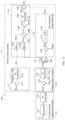
- FIG. 3 is a detailed functional-block diagram of the switch control device 11 shown in FIG. 2 .
- the circular-current suppression module 21 includes a calculator 31 and a proportional-integral (PI) controller 32.
- the voltage balance module 22 includes a subtractor 33 and a PI controller 34.
- the subtractor 33 is connected to the PI controller 32 of the circular-current suppression module 21 and is configured to subtract the bus-voltage difference ⁇ V bus from the first reference voltage V m,ref to generate a difference.
- the PI controller 34 is connected to the subtractor 33 and is configured to convert the difference between the first reference voltage V m,ref and the bus-voltage difference ⁇ V bus into the first reference current i m,ref .
- the switch control module 23 includes a selector 35, a zero-sequence voltage injection module 36, a total DC voltage module 37, and a plurality of current control modules 38.
- the selector 35 is connected to the PI controller 34 of the voltage balance module 22 and is configured to output the first reference current i m,ref to the zero-sequence voltage injection module 36 or the plurality of current control modules 38 according to a control command CC.
- the zero-sequence voltage injection module 36 is connected to the selector 35 and is configured to generate a zero-sequence voltage V zero according to the first reference current i m,ref and the target voltage V target .
- the selector 35 outputs the first reference current i m,ref to the plurality of current control modules 38, such that the plurality of current control modules 38 generate the plurality of switching commands D LR , D LS , and D LT according to the first reference current i m,ref ; in another aspect, in a zero-sequence voltage injection mode, the selector 35 outputs the first reference current i m,ref to the zero-sequence voltage injection module 36, such that the plurality of current control module 38 generate the plurality of switching commands D LR , D LS , and D LT according to the zero-sequence voltage V zero .
- the zero-sequence voltage injection module 36 includes a subtractor 361 and a gain amplifier 362.
- the subtractor 361 is connected to the selector 35 and is configured to subtract the target voltage V target from a voltage corresponding to the first reference current i m,ref to generate a third reference voltage V z,ref .
- an magnitude of the target voltage V target is zero to instruct the zero-sequence voltage injection module 36 to converge the voltage corresponding to the first reference current i m,ref until it is converged to zero; in another embodiment, according to actual application requirements, the magnitude of the target voltage V target is a tolerance value that is not zero.
- the gain amplifier 362 is connected to the subtractor 361 and is configured to multiply the third reference voltage V z,ref by a coefficient (-K p ) to generate the zero-sequence voltage V zero , wherein the coefficient K p can be anyone real number.
- the total DC voltage module 37 includes a subtractor 371 and a PI controller 372.
- the subtractor 371 is configured to subtract the total voltage V total from the second reference voltage V ref .
- the PI controller 372 is connected to the subtractor 371 and is configured to convert a difference between the second reference voltage V ref and the total voltage V total into a total direct current i dc .
- the sine function generator 381 is connected to the total DC voltage module 37 and is configured to extract the sine integer-harmonic component i har,dc of the total DC current i dc , wherein the angular frequency of the sine integer harmonics is ⁇ .
- the cosine function generator 383 is connected to the selector 35 and is configured to extract the cosine even-numbered harmonic components i har,ref of the first reference current i m,ref , wherein the angular frequency of the even-numbered harmonics is (E*2* ⁇ ), and E is a natural number.
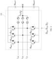
- the power factor corrector 13 of FIG. 1 can be implemented by using a T-type neutral-point-clamping (NPC) architecture, such as the power factor corrector 13 shown in FIG. 4 .
- NPC neutral-point-clamping
- the power factor corrector 13 is configured to generate an output current i m,PFC according to the input currents i LR , i LS , and i LT and the plurality of switching commands D LR , D LS , and D LT to charge the two bus capacitors to adjust the positive bus voltage V bus,P and the negative bus voltage V bus,N .
- the power factor corrector 13 generates a duty-cycle signal group for turning on (ON) and turning off (OFF) a switch group according to the plurality of switching control functions
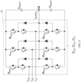
- the power factor corrector 13 of FIG. 1 can be implemented by using an I-type neutral-point-clamping architecture, such as the power factor corrector 63 shown in FIG. 6 .
- the power factor corrector 63 is configured to generate an output current i m,PFC according to the input currents i LR , i LS , and i LT and the plurality of switching commands D LR , D LS , and D LT to charge the two bus capacitors to adjust the positive bus voltage V bus,P and the negative bus voltage V bus,N .
- a theoretical mathematical model of the output current i m,PFC of the power factor corrector 63 please refer to the relevant description of FIG. 4 mentioned as above, which is not be described again here.
- the input current i LS flows to the positive terminal P through the positive half-cycle path, causing the positive bus voltage V bus,P1' to rise and the negative bus voltage V bus,N1' to remain the same. In the case of the total voltage remaining the same, the terminal voltage V bus,M1' of the neutral terminal M drops.
- the input current i LS flows to the negative terminal N through the negative half-cycle path, causing the negative bus voltage V bus,N2' to drop and the positive bus voltage V bus,P2' to remain the same. In the case of the total voltage remaining the same, the terminal voltage V bus,M2' of the neutral terminal M drops.
- the input current i LS flows to the neutral terminal M through a first intermediate path of lower-arm switches, because the input current i LS does not go through the bus capacitors, the positive bus voltage V bus,P31' and the negative bus voltage V bus,N31' do not increase or decrease. In the case of the total voltage remaining the same, the terminal voltage V bus,M31' of the neutral terminal M remains at a specific value.
- the input current i LS flows to the neutral terminal M through a second intermediate path of upper-arm switches, because the input current i LS does not go through the bus capacitors, the positive bus voltage V bus,P32' and the negative bus voltage V bus,N32' do not increase or decrease.
- the terminal voltage V bus,M32' of the neutral terminal M remains at a specific value. Therefore, by using the switching command D LS , the bus voltage and the terminal voltage of the neutral terminal M can be effectively adjusted to balance the negative bus voltage and suppress the circular current.
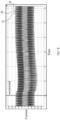
- FIGs. 8 and 9 are diagrams illustrating current and bus voltage waveforms of the switch control device in FIG. 1 in a process of performing circular current suppression.
- inductor currents I1, I2, and I3 taken out from the power factor corrector 13 correspond to the three-phase electric power (such as R, S, and T phases), respectively.
- the inductor currents I1, I2, and I3 gradually rise until the magnitudes of the inductor currents I1, I2, and I3 return to the preset values.
- Each switching control device 101 is configured to generate a switching command D L according to the input currents i 1 and i 2 , the positive bus voltage Vci, and the negative bus voltage V C2 .
- the circular-current suppression module 111 first calculates the circular current corresponding to the input currents i L and i N and converts it into the first reference voltage V n,ref .
- the voltage balance module 112 calculates a difference between the first reference voltage V n,ref and the bus-voltage difference ⁇ V bus based on the first reference voltage V n,ref and converts it into the first reference current i m,ref .
- the switch control module 113 generates a switching command D L to the power factor corrector 103 according to the first reference current i m,ref .
- the switch control device 101 can converge the circular current to the target current i target (e.g., zero ampere) and converge the bus-voltage difference ⁇ V bus to the target voltage V target (e.g., zero volts), thereby achieving the effect of suppressing the circular current.
- the target current i target e.g., zero ampere
- ⁇ V bus the target voltage V target
- FIG. 12 is a detailed functional-block diagram of the switch control device 101 shown in FIG. 11 .
- the circular-current suppression module 111 includes a calculator 121 and a proportional-integral (PI) controller 122.
- i L is one live-wire current among the plurality of input currents
- i N is a neutral-current among the plurality of input currents
- the calculator 121 is configured to calculate the average value of the input currents i L and i N to calculate the common-mode current i z to detect the circular current.
- the PI controller 122 is connected to the calculator 121 and is configured to convert the common-mode current i z to the first reference voltage V n,ref .
- the voltage balance module 112 includes a subtractor 123 and a PI controller 124.
- the subtractor 123 is connected to the PI controller 122 of the circular-current suppression module 111 and is configured to subtract the bus-voltage difference ⁇ V bus from the first reference voltage V n,ref to generate a difference.
- the PI controller 124 is connected to the subtractor 123 and is configured to convert the difference between the first reference voltage V n,ref and the bus-voltage difference ⁇ V bus into the first reference current i m,ref .
- the switch control module 113 includes a selector 115, a zero-sequence voltage injection module 116, a total DC voltage module 117, and a current control module 118.
- the selector 115 is connected to the PI controller 124 of the voltage balance module 112 and is configured to output the first reference current i m,ref to the zero-sequence voltage injection module 116 or the current control module 118 according to a control command CC.
- the zero-sequence voltage injection module 116 is connected to the selector 115 and is configured to generate a zero-sequence voltage V zero according to the first reference current i m,ref .
- the current control module 118 is connected to the total DC voltage module 117, the selector 115, and the zero-sequence voltage injection module 116 and is configured to generate the switching command DL according to the total DC current i dc , the input currents i L and i N , and the first reference current i m,ref or according to the zero-sequence voltage V zero .
- the selector 115 outputs the first reference current i m,ref to the current control module 118, such that the current control module 118 generates the switching command D L according to the first reference current i m,ref ; in another aspect, in a zero-sequence voltage injection mode, the selector 115 outputs the first reference current i m,ref to the zero-sequence voltage injection module 116, such that the current control module 118 generate the switching command D L according to the zero-sequence voltage V zero .
- the zero-sequence voltage injection module 116 includes an adder 1160, an inverter 1161, and a gain amplifier 1162.
- the adder 1160 is connected to the selector 115 and is configured to calculate a sum of a voltage corresponding to the first reference current i m,ref and the target voltage V target (e.g., zero) to generate the third reference voltage V z,ref .
- the adder 1160 can be replaced by a subtractor to converge the voltage corresponding to the first reference current i m,ref to the target voltage V target .
- the total DC voltage module 117 includes a subtractor 1171 and a PI controller 1172.
- the subtractor 1171 is configured to subtract the total voltage V total from the second reference voltage V ref .
- the PI controller 1172 is connected to the subtractor 1171 and is configured to convert a difference between the second reference voltage V ref and the total voltage V total into a total direct current i dc .
- the current control module 118 is configured to generate switching command D L .
- the current control module 118 includes a sine function generator 1181, a cosine function generator 1183, an adder 1184, a subtractor 1185, a PI controller 1186, and an adder 1187.
- the sine function generator 1181 is connected to the total DC voltage module 117 and is configured to extract the sine integer-harmonic component i har,dc of the total DC current i dc , wherein the angular frequency of the sine integer harmonics is ⁇ .
- the cosine function generator 1183 is connected to the selector 115 and is configured to extract the cosine even-numbered harmonic components i har,ref of the first reference current i m,ref , wherein the angular frequency of the even-numbered harmonics is (E*2* ⁇ ), and E is a natural number.
- the adder 1184 is connected to the sine function generator 1181 and the cosine function generator 1183 and is configured to add the target current i target , the sine integer-harmonic component i har,dc , and the cosine even-numbered harmonic components i har,ref to generate a second reference current i L,ref .
- the magnitude of the target current i target is zero to instruct the current control module 118 to converge the first reference current i m,ref until it is converged to zero; in other embodiments, according to actual application requirements, the magnitude of the target current i target is a tolerance value that is not zero.
- the PI controller 1186 is connected to the subtractor 1185 and is configured to convert the compensation current i comp into a compensation voltage V comp .
- the adder 1187 is connected to the PI controller 1186 and is configured to add the compensation voltage V comp and the zero-sequence voltage V zero to generate the switching command D L .
- the power factor corrector 103 may be implemented by using a T-type neutral-point-clamping architecture, as shown in FIG. 13 .
- a circuit is simplified, and not all components of the power factor corrector 103 are shown in FIG. 13 .
- the power factor corrector 103 is configured to generate an output current i m,PFC according to the input currents i L and i N and the switching command D L to charge the two bus capacitors to adjust the positive bus voltage Vci and the negative bus voltage V C2 .
- the power factor corrector 103 can be adopted to inject active current or zero-sequence voltage into at least one of the positive bus capacitor C1 and the negative bus capacitor C2 (as shown in FIG. 10 ) , thereby adjusting at least one of the positive bus voltage V C1 and the negative bus voltage V C2 .
- the power factor corrector 103 generates a duty-period signal group for turning on and off a switch group according to the plurality of switching control functions
- d a 2 ⁇ A ⁇ 4 A ⁇ 1 3 cos 2 ⁇ t + 1 15 cos 4 ⁇ t + ...
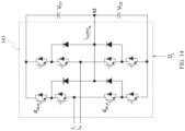
- the power factor corrector 103 of FIG. 10 can be implemented by using an I-type neutral-point-clamping architecture, such as a power factor corrector 143 shown in FIG. 14 .
- a circuit is simplified, and not all components of the power factor corrector 143 are shown in FIG. 14 .
- the power factor corrector 143 is configured to generate an output current i m,PFC according to the input currents i L and i N and a switching command D L to charge the two bus capacitors to adjust the positive bus voltage Vci and the negative bus capacitance V C2 .
- the theoretical mathematical model of the output current i m,PFC of the power factor corrector 103 please refer to the relevant description of FIG. 13 mentioned as above, and will not be described again here.
- the switching control device 101 can generate the switching command D L according to function (4-a') to balance the negative bus voltage V bus,N to suppress circular current.
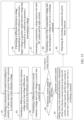
- Step S1 calculating a common-mode current according to a plurality of input currents to convert into a first reference voltage.
- Step S4 determining whether a harmonic current control mode or a zero-sequence voltage injection mode is performed. If the harmonic current control mode is performed, proceed to step S5; if the zero-sequence voltage injection mode is performed, then proceed to step S6.
- Step S5 adding the cosine even-numbered harmonic components of the first reference current based on the total DC current, the target current, and the input currents to convert into a compensation voltage to serve as a switching command. Then, proceed to step S9.
- Step S6 calculating a difference between a voltage corresponding to the first reference current and a target voltage to multiply the difference by a coefficient to generate a zero sequence voltage.
- Step S7 generating a compensation voltage based on the total DC current and the input currents.
- Step S8 calculating a sum of the compensation voltage and the zero-sequence voltage to serve as a switching command.
- Step S9 outputting the switching command to the power factor corrector. Then, returning to step S1. It should be understood that the circular current suppression method terminates execution when a termination condition is met, such as when the power conversion system terminates operations.
- step S3 the total DC voltage module 37 calculates the difference between the second reference voltage V ref and the total voltage V total to convert into the total DC current i dc .
- step S4 the selector 35 determines whether the harmonic current control mode or the zero-sequence voltage injection mode is performed according to the control command CC.
- step S5 in the harmonic current control mode, the current control module 38 adds the cosine even-numbered harmonic components i har,ref of the first reference current i m,ref based on the total DC current i dc , the target current i target , and the input currents (e.g., one of i LR , i LS , and i LT ) to convert into the compensation voltage V comp to serve as the switching command (e.g., one of D LR , D LS and D LT ).
- the input currents e.g., one of i LR , i LS , and i LT
- step S8 the current control module 38 calculates the sum of the compensation voltage V comp and the zero-sequence voltage V zero to serve as the switching command (such as one of D LR , D LS , and D LT ).
- the selector 35 inputs the first reference current i m,ref to the zero-sequence voltage injection module 36, such the compensation voltage V comp only includes the sine integer-harmonic component i har,dc of the total direct current i dc .
- step S9 in the harmonic current control mode and zero sequence voltage injection mode, the current control module 38 outputs switching commands (such as one of D LR , D LS , and D LT ) to the power factor corrector 13.
- switching commands such as one of D LR , D LS , and D LT
Landscapes
- Engineering & Computer Science (AREA)
- Power Engineering (AREA)
- Inverter Devices (AREA)
- Rectifiers (AREA)
Applications Claiming Priority (1)
| Application Number | Priority Date | Filing Date | Title |
|---|---|---|---|
| CN202410010997.2A CN120262883A (zh) | 2024-01-04 | 2024-01-04 | 环流抑制方法、开关控制装置及电力转换系统 |
Publications (1)
| Publication Number | Publication Date |
|---|---|
| EP4583383A1 true EP4583383A1 (de) | 2025-07-09 |
Family
ID=93704899
Family Applications (1)
| Application Number | Title | Priority Date | Filing Date |
|---|---|---|---|
| EP24215736.0A Pending EP4583383A1 (de) | 2024-01-04 | 2024-11-27 | Kreisstromunterdrückungsverfahren und schaltersteuerungsvorrichtung |
Country Status (3)
| Country | Link |
|---|---|
| US (1) | US20250226739A1 (de) |
| EP (1) | EP4583383A1 (de) |
| CN (1) | CN120262883A (de) |
Citations (3)
| Publication number | Priority date | Publication date | Assignee | Title |
|---|---|---|---|---|
| CN104065255A (zh) * | 2014-03-24 | 2014-09-24 | 南京航空航天大学 | 一种基于零序环流前馈的并联三相四桥臂逆变器环流抑制方法 |
| CN115864872A (zh) * | 2023-01-06 | 2023-03-28 | 电子科技大学长三角研究院(湖州) | 一种面向并联t型三电平整流器的公平顺序模型预测控制多目标优化方法 |
| CN116827086A (zh) * | 2023-07-03 | 2023-09-29 | 华为数字能源技术有限公司 | 功率转换装置和充电装置 |
Family Cites Families (4)
| Publication number | Priority date | Publication date | Assignee | Title |
|---|---|---|---|---|
| US10797589B2 (en) * | 2017-09-28 | 2020-10-06 | Texas Instruments Incorporated | Methods and apparatus to compensate for power factor loss using a phasor cancellation based compensation scheme |
| CN112909946B (zh) * | 2021-01-29 | 2024-05-28 | 国网上海市电力公司 | 一种注入共模电压与环流的mmc子模块电压波动抑制方法 |
| CN116827156A (zh) * | 2023-07-12 | 2023-09-29 | 华为数字能源技术有限公司 | 功率变换器、储能系统和控制方法 |
| CN119995328A (zh) * | 2023-11-10 | 2025-05-13 | 山特电子(深圳)有限公司 | 谐波衰减系统以及包括其的不间断电源 |
-
2024
- 2024-01-04 CN CN202410010997.2A patent/CN120262883A/zh active Pending
- 2024-10-24 US US18/925,120 patent/US20250226739A1/en active Pending
- 2024-11-27 EP EP24215736.0A patent/EP4583383A1/de active Pending
Patent Citations (4)
| Publication number | Priority date | Publication date | Assignee | Title |
|---|---|---|---|---|
| CN104065255A (zh) * | 2014-03-24 | 2014-09-24 | 南京航空航天大学 | 一种基于零序环流前馈的并联三相四桥臂逆变器环流抑制方法 |
| CN115864872A (zh) * | 2023-01-06 | 2023-03-28 | 电子科技大学长三角研究院(湖州) | 一种面向并联t型三电平整流器的公平顺序模型预测控制多目标优化方法 |
| CN116827086A (zh) * | 2023-07-03 | 2023-09-29 | 华为数字能源技术有限公司 | 功率转换装置和充电装置 |
| EP4506204A2 (de) * | 2023-07-03 | 2025-02-12 | Huawei Digital Power Technologies Co., Ltd. | Leistungsumwandlungsvorrichtung und ladevorrichtung |
Non-Patent Citations (2)
| Title |
|---|
| NARIMANI MEHDI ET AL: "Three-Phase Multimodule VSIs Using SHE-PWM to Reduce Zero-Sequence Circulating Current", IEEE TRANSACTIONS ON INDUSTRIAL ELECTRONICS, IEEE SERVICE CENTER, PISCATAWAY, NJ, USA, vol. 61, no. 4, 1 April 2014 (2014-04-01), pages 1659 - 1668, XP011531105, ISSN: 0278-0046, [retrieved on 20131022], DOI: 10.1109/TIE.2013.2267706 * |
| SUN KAI ET AL: "Improved Modulation Mechanism of Parallel-Operated T-Type Three-Level PWM Rectifiers for Neutral-Point Potential Balancing and Circulating Current Suppression", IEEE TRANSACTIONS ON POWER ELECTRONICS, INSTITUTE OF ELECTRICAL AND ELECTRONICS ENGINEERS, USA, vol. 33, no. 9, 1 September 2018 (2018-09-01), pages 7466 - 7479, XP011686275, ISSN: 0885-8993, [retrieved on 20180629], DOI: 10.1109/TPEL.2017.2772025 * |
Also Published As
| Publication number | Publication date |
|---|---|
| CN120262883A (zh) | 2025-07-04 |
| US20250226739A1 (en) | 2025-07-10 |
Similar Documents
| Publication | Publication Date | Title |
|---|---|---|
| Wei et al. | A circulating-current suppression method for parallel-connected voltage-source inverters with common DC and AC buses | |
| Wang et al. | Topologies and control strategies of cascaded bridgeless multilevel rectifiers | |
| US20110134672A1 (en) | Power conversion apparatus | |
| Chen et al. | Modified interleaved current sensorless control for three-level boost PFC converter with considering voltage imbalance and zero-crossing current distortion | |
| RU2732541C1 (ru) | Способ управления трехфазным виенна-выпрямителем | |
| WO2021186524A1 (ja) | 電力変換装置 | |
| CN105379096A (zh) | 有关将电力从dc电力线分接到ac电力线的布置、方法和计算机程序产品 | |
| Liao et al. | Notice of Violation of IEEE Publication Principles: Single-Phase Common-Ground-Type Transformerless PV Grid-Connected Inverters | |
| JPWO2019215842A1 (ja) | 電力変換装置 | |
| Naik et al. | A new two-phase five-level converter for three-phase isolated grid-tied systems with inherent capacitor balancing and reduced component count | |
| Iman-Eini et al. | Design of power electronic transformer based on cascaded H-bridge multilevel converter | |
| CN115241926B (zh) | 母线电压控制方法、母线平衡控制方法及其系统 | |
| US20250226739A1 (en) | Circular current suppression method, switch control device, and power conversion system | |
| Patil et al. | A novel electric vehicle charging station based on parallel hybrid converter and DAB with ability to simultaneously work in STATCOM Mode | |
| Pan et al. | Modeling of circulating currents for grid-connected parallel three-phase inverters | |
| Wong et al. | Voltage balance control of cascaded H-bridge rectifier-based solid-state transformer with vector refactoring technology in αβ frame | |
| Cheng et al. | A modified one cycle control of Vienna rectifier for neutral point voltage balancing control based on cycle-by-cycle correction | |
| TWI872904B (zh) | 環流抑制方法、開關控制裝置及電力轉換系統 | |
| CN111934572B (zh) | 一种超大规模储能mmc变换器装置及储能控制方法 | |
| Patil et al. | A novel multilevel ev charging station based on the parallel hybrid converter and dual active bridge | |
| Huang et al. | An automatic power decoupling control method on three level DC-AC converter to suppress the double-line-frequency ripple | |
| CN114172166A (zh) | 一种电压发生装置及其高频发生控制方法 | |
| Kumar et al. | Current sharing control strategy of parallel inverters using instantaneous symmetrical component theory | |
| Kim et al. | Selective Control Algorithm for N-Phase Switching Power Pole of 4-Leg Interlinking Converter in AC/DC Hybrid Microgrid | |
| Jagadeesh et al. | ZSI supported DSTATCOM for Plug-in Electrical Vehicle charging station |
Legal Events
| Date | Code | Title | Description |
|---|---|---|---|
| PUAI | Public reference made under article 153(3) epc to a published international application that has entered the european phase |
Free format text: ORIGINAL CODE: 0009012 |
|
| STAA | Information on the status of an ep patent application or granted ep patent |
Free format text: STATUS: THE APPLICATION HAS BEEN PUBLISHED |
|
| AK | Designated contracting states |
Kind code of ref document: A1 Designated state(s): AL AT BE BG CH CY CZ DE DK EE ES FI FR GB GR HR HU IE IS IT LI LT LU LV MC ME MK MT NL NO PL PT RO RS SE SI SK SM TR |
|
| STAA | Information on the status of an ep patent application or granted ep patent |
Free format text: STATUS: REQUEST FOR EXAMINATION WAS MADE |
|
| 17P | Request for examination filed |
Effective date: 20251128 |
|
| STAA | Information on the status of an ep patent application or granted ep patent |
Free format text: STATUS: EXAMINATION IS IN PROGRESS |
|
| 17Q | First examination report despatched |
Effective date: 20260317 |