EP4583666A2 - Halbleiteranordnung - Google Patents
Halbleiteranordnung Download PDFInfo
- Publication number
- EP4583666A2 EP4583666A2 EP25178310.6A EP25178310A EP4583666A2 EP 4583666 A2 EP4583666 A2 EP 4583666A2 EP 25178310 A EP25178310 A EP 25178310A EP 4583666 A2 EP4583666 A2 EP 4583666A2
- Authority
- EP
- European Patent Office
- Prior art keywords
- region
- gate
- built
- resistor
- semiconductor device
- Prior art date
- Legal status (The legal status is an assumption and is not a legal conclusion. Google has not performed a legal analysis and makes no representation as to the accuracy of the status listed.)
- Pending
Links
Images



Classifications
-
- H—ELECTRICITY
- H10—SEMICONDUCTOR DEVICES; ELECTRIC SOLID-STATE DEVICES NOT OTHERWISE PROVIDED FOR
- H10D—INORGANIC ELECTRIC SEMICONDUCTOR DEVICES
- H10D84/00—Integrated devices formed in or on semiconductor substrates that comprise only semiconducting layers, e.g. on Si wafers or on GaAs-on-Si wafers
- H10D84/90—Masterslice integrated circuits
- H10D84/998—Input and output buffer/driver structures
-
- H—ELECTRICITY
- H10—SEMICONDUCTOR DEVICES; ELECTRIC SOLID-STATE DEVICES NOT OTHERWISE PROVIDED FOR
- H10D—INORGANIC ELECTRIC SEMICONDUCTOR DEVICES
- H10D12/00—Bipolar devices controlled by the field effect, e.g. insulated-gate bipolar transistors [IGBT]
- H10D12/411—Insulated-gate bipolar transistors [IGBT]
- H10D12/441—Vertical IGBTs
-
- H—ELECTRICITY
- H10—SEMICONDUCTOR DEVICES; ELECTRIC SOLID-STATE DEVICES NOT OTHERWISE PROVIDED FOR
- H10D—INORGANIC ELECTRIC SEMICONDUCTOR DEVICES
- H10D12/00—Bipolar devices controlled by the field effect, e.g. insulated-gate bipolar transistors [IGBT]
- H10D12/411—Insulated-gate bipolar transistors [IGBT]
- H10D12/441—Vertical IGBTs
- H10D12/461—Vertical IGBTs having non-planar surfaces, e.g. having trenches, recesses or pillars in the surfaces of the emitter, base or collector regions
- H10D12/481—Vertical IGBTs having non-planar surfaces, e.g. having trenches, recesses or pillars in the surfaces of the emitter, base or collector regions having gate structures on slanted surfaces, on vertical surfaces, or in grooves, e.g. trench gate IGBTs
-
- H—ELECTRICITY
- H10—SEMICONDUCTOR DEVICES; ELECTRIC SOLID-STATE DEVICES NOT OTHERWISE PROVIDED FOR
- H10D—INORGANIC ELECTRIC SEMICONDUCTOR DEVICES
- H10D30/00—Field-effect transistors [FET]
- H10D30/60—Insulated-gate field-effect transistors [IGFET]
- H10D30/64—Double-diffused metal-oxide semiconductor [DMOS] FETs
- H10D30/66—Vertical DMOS [VDMOS] FETs
- H10D30/665—Vertical DMOS [VDMOS] FETs having edge termination structures
-
- H—ELECTRICITY
- H10—SEMICONDUCTOR DEVICES; ELECTRIC SOLID-STATE DEVICES NOT OTHERWISE PROVIDED FOR
- H10D—INORGANIC ELECTRIC SEMICONDUCTOR DEVICES
- H10D30/00—Field-effect transistors [FET]
- H10D30/60—Insulated-gate field-effect transistors [IGFET]
- H10D30/64—Double-diffused metal-oxide semiconductor [DMOS] FETs
- H10D30/66—Vertical DMOS [VDMOS] FETs
- H10D30/668—Vertical DMOS [VDMOS] FETs having trench gate electrodes, e.g. UMOS transistors
-
- H—ELECTRICITY
- H10—SEMICONDUCTOR DEVICES; ELECTRIC SOLID-STATE DEVICES NOT OTHERWISE PROVIDED FOR
- H10D—INORGANIC ELECTRIC SEMICONDUCTOR DEVICES
- H10D62/00—Semiconductor bodies, or regions thereof, of devices having potential barriers
- H10D62/80—Semiconductor bodies, or regions thereof, of devices having potential barriers characterised by the materials
- H10D62/83—Semiconductor bodies, or regions thereof, of devices having potential barriers characterised by the materials being Group IV materials, e.g. B-doped Si or undoped Ge
- H10D62/832—Semiconductor bodies, or regions thereof, of devices having potential barriers characterised by the materials being Group IV materials, e.g. B-doped Si or undoped Ge being Group IV materials comprising two or more elements, e.g. SiGe
- H10D62/8325—Silicon carbide
-
- H—ELECTRICITY
- H10—SEMICONDUCTOR DEVICES; ELECTRIC SOLID-STATE DEVICES NOT OTHERWISE PROVIDED FOR
- H10D—INORGANIC ELECTRIC SEMICONDUCTOR DEVICES
- H10D64/00—Electrodes of devices having potential barriers
- H10D64/20—Electrodes characterised by their shapes, relative sizes or dispositions
- H10D64/27—Electrodes not carrying the current to be rectified, amplified, oscillated or switched, e.g. gates
- H10D64/311—Gate electrodes for field-effect devices
- H10D64/411—Gate electrodes for field-effect devices for FETs
- H10D64/511—Gate electrodes for field-effect devices for FETs for IGFETs
- H10D64/517—Gate electrodes for field-effect devices for FETs for IGFETs characterised by the conducting layers
-
- H—ELECTRICITY
- H10—SEMICONDUCTOR DEVICES; ELECTRIC SOLID-STATE DEVICES NOT OTHERWISE PROVIDED FOR
- H10D—INORGANIC ELECTRIC SEMICONDUCTOR DEVICES
- H10D84/00—Integrated devices formed in or on semiconductor substrates that comprise only semiconducting layers, e.g. on Si wafers or on GaAs-on-Si wafers
- H10D84/101—Integrated devices comprising main components and built-in components, e.g. IGBT having built-in freewheel diode
- H10D84/141—VDMOS having built-in components
-
- H—ELECTRICITY
- H10—SEMICONDUCTOR DEVICES; ELECTRIC SOLID-STATE DEVICES NOT OTHERWISE PROVIDED FOR
- H10D—INORGANIC ELECTRIC SEMICONDUCTOR DEVICES
- H10D84/00—Integrated devices formed in or on semiconductor substrates that comprise only semiconducting layers, e.g. on Si wafers or on GaAs-on-Si wafers
- H10D84/90—Masterslice integrated circuits
- H10D84/903—Masterslice integrated circuits comprising field effect technology
- H10D84/907—CMOS gate arrays
-
- H—ELECTRICITY
- H10—SEMICONDUCTOR DEVICES; ELECTRIC SOLID-STATE DEVICES NOT OTHERWISE PROVIDED FOR
- H10D—INORGANIC ELECTRIC SEMICONDUCTOR DEVICES
- H10D84/00—Integrated devices formed in or on semiconductor substrates that comprise only semiconducting layers, e.g. on Si wafers or on GaAs-on-Si wafers
- H10D84/90—Masterslice integrated circuits
- H10D84/996—Masterslice integrated circuits using combined field effect technology and bipolar technology
-
- H—ELECTRICITY
- H10—SEMICONDUCTOR DEVICES; ELECTRIC SOLID-STATE DEVICES NOT OTHERWISE PROVIDED FOR
- H10W—GENERIC PACKAGES, INTERCONNECTIONS, CONNECTORS OR OTHER CONSTRUCTIONAL DETAILS OF DEVICES COVERED BY CLASS H10
- H10W20/00—Interconnections in chips, wafers or substrates
- H10W20/40—Interconnections external to wafers or substrates, e.g. back-end-of-line [BEOL] metallisations or vias connecting to gate electrodes
- H10W20/41—Interconnections external to wafers or substrates, e.g. back-end-of-line [BEOL] metallisations or vias connecting to gate electrodes characterised by their conductive parts
- H10W20/43—Layouts of interconnections
-
- H—ELECTRICITY
- H10—SEMICONDUCTOR DEVICES; ELECTRIC SOLID-STATE DEVICES NOT OTHERWISE PROVIDED FOR
- H10D—INORGANIC ELECTRIC SEMICONDUCTOR DEVICES
- H10D30/00—Field-effect transistors [FET]
- H10D30/60—Insulated-gate field-effect transistors [IGFET]
-
- H—ELECTRICITY
- H10—SEMICONDUCTOR DEVICES; ELECTRIC SOLID-STATE DEVICES NOT OTHERWISE PROVIDED FOR
- H10D—INORGANIC ELECTRIC SEMICONDUCTOR DEVICES
- H10D62/00—Semiconductor bodies, or regions thereof, of devices having potential barriers
- H10D62/10—Shapes, relative sizes or dispositions of the regions of the semiconductor bodies; Shapes of the semiconductor bodies
- H10D62/102—Constructional design considerations for preventing surface leakage or controlling electric field concentration
- H10D62/103—Constructional design considerations for preventing surface leakage or controlling electric field concentration for increasing or controlling the breakdown voltage of reverse-biased devices
- H10D62/105—Constructional design considerations for preventing surface leakage or controlling electric field concentration for increasing or controlling the breakdown voltage of reverse-biased devices by having particular doping profiles, shapes or arrangements of PN junctions; by having supplementary regions, e.g. junction termination extension [JTE]
-
- H—ELECTRICITY
- H10—SEMICONDUCTOR DEVICES; ELECTRIC SOLID-STATE DEVICES NOT OTHERWISE PROVIDED FOR
- H10D—INORGANIC ELECTRIC SEMICONDUCTOR DEVICES
- H10D62/00—Semiconductor bodies, or regions thereof, of devices having potential barriers
- H10D62/10—Shapes, relative sizes or dispositions of the regions of the semiconductor bodies; Shapes of the semiconductor bodies
- H10D62/124—Shapes, relative sizes or dispositions of the regions of semiconductor bodies or of junctions between the regions
- H10D62/126—Top-view geometrical layouts of the regions or the junctions
- H10D62/127—Top-view geometrical layouts of the regions or the junctions of cellular field-effect devices, e.g. multicellular DMOS transistors or IGBTs
-
- H—ELECTRICITY
- H10—SEMICONDUCTOR DEVICES; ELECTRIC SOLID-STATE DEVICES NOT OTHERWISE PROVIDED FOR
- H10D—INORGANIC ELECTRIC SEMICONDUCTOR DEVICES
- H10D62/00—Semiconductor bodies, or regions thereof, of devices having potential barriers
- H10D62/10—Shapes, relative sizes or dispositions of the regions of the semiconductor bodies; Shapes of the semiconductor bodies
- H10D62/17—Semiconductor regions connected to electrodes not carrying current to be rectified, amplified or switched, e.g. channel regions
- H10D62/393—Body regions of DMOS transistors or IGBTs
-
- H—ELECTRICITY
- H10—SEMICONDUCTOR DEVICES; ELECTRIC SOLID-STATE DEVICES NOT OTHERWISE PROVIDED FOR
- H10D—INORGANIC ELECTRIC SEMICONDUCTOR DEVICES
- H10D64/00—Electrodes of devices having potential barriers
- H10D64/20—Electrodes characterised by their shapes, relative sizes or dispositions
- H10D64/27—Electrodes not carrying the current to be rectified, amplified, oscillated or switched, e.g. gates
- H10D64/311—Gate electrodes for field-effect devices
- H10D64/411—Gate electrodes for field-effect devices for FETs
- H10D64/511—Gate electrodes for field-effect devices for FETs for IGFETs
- H10D64/512—Disposition of the gate electrodes, e.g. buried gates
- H10D64/513—Disposition of the gate electrodes, e.g. buried gates within recesses in the substrate, e.g. trench gates, groove gates or buried gates
-
- H—ELECTRICITY
- H10—SEMICONDUCTOR DEVICES; ELECTRIC SOLID-STATE DEVICES NOT OTHERWISE PROVIDED FOR
- H10D—INORGANIC ELECTRIC SEMICONDUCTOR DEVICES
- H10D64/00—Electrodes of devices having potential barriers
- H10D64/20—Electrodes characterised by their shapes, relative sizes or dispositions
- H10D64/27—Electrodes not carrying the current to be rectified, amplified, oscillated or switched, e.g. gates
- H10D64/311—Gate electrodes for field-effect devices
- H10D64/411—Gate electrodes for field-effect devices for FETs
- H10D64/511—Gate electrodes for field-effect devices for FETs for IGFETs
- H10D64/517—Gate electrodes for field-effect devices for FETs for IGFETs characterised by the conducting layers
- H10D64/519—Gate electrodes for field-effect devices for FETs for IGFETs characterised by the conducting layers characterised by their top-view geometrical layouts
-
- H—ELECTRICITY
- H10—SEMICONDUCTOR DEVICES; ELECTRIC SOLID-STATE DEVICES NOT OTHERWISE PROVIDED FOR
- H10D—INORGANIC ELECTRIC SEMICONDUCTOR DEVICES
- H10D84/00—Integrated devices formed in or on semiconductor substrates that comprise only semiconducting layers, e.g. on Si wafers or on GaAs-on-Si wafers
- H10D84/90—Masterslice integrated circuits
- H10D84/903—Masterslice integrated circuits comprising field effect technology
- H10D84/907—CMOS gate arrays
- H10D84/909—Microarchitecture
- H10D84/959—Connectability characteristics, i.e. diffusion and polysilicon geometries
- H10D84/966—Gate electrode terminals or contacts
-
- H—ELECTRICITY
- H10—SEMICONDUCTOR DEVICES; ELECTRIC SOLID-STATE DEVICES NOT OTHERWISE PROVIDED FOR
- H10W—GENERIC PACKAGES, INTERCONNECTIONS, CONNECTORS OR OTHER CONSTRUCTIONAL DETAILS OF DEVICES COVERED BY CLASS H10
- H10W20/00—Interconnections in chips, wafers or substrates
- H10W20/40—Interconnections external to wafers or substrates, e.g. back-end-of-line [BEOL] metallisations or vias connecting to gate electrodes
- H10W20/41—Interconnections external to wafers or substrates, e.g. back-end-of-line [BEOL] metallisations or vias connecting to gate electrodes characterised by their conductive parts
- H10W20/44—Conductive materials thereof
- H10W20/4403—Conductive materials thereof based on metals, e.g. alloys, metal silicides
- H10W20/4405—Conductive materials thereof based on metals, e.g. alloys, metal silicides the principal metal being aluminium
-
- H—ELECTRICITY
- H10—SEMICONDUCTOR DEVICES; ELECTRIC SOLID-STATE DEVICES NOT OTHERWISE PROVIDED FOR
- H10W—GENERIC PACKAGES, INTERCONNECTIONS, CONNECTORS OR OTHER CONSTRUCTIONAL DETAILS OF DEVICES COVERED BY CLASS H10
- H10W20/00—Interconnections in chips, wafers or substrates
- H10W20/40—Interconnections external to wafers or substrates, e.g. back-end-of-line [BEOL] metallisations or vias connecting to gate electrodes
- H10W20/41—Interconnections external to wafers or substrates, e.g. back-end-of-line [BEOL] metallisations or vias connecting to gate electrodes characterised by their conductive parts
- H10W20/44—Conductive materials thereof
- H10W20/4403—Conductive materials thereof based on metals, e.g. alloys, metal silicides
- H10W20/4405—Conductive materials thereof based on metals, e.g. alloys, metal silicides the principal metal being aluminium
- H10W20/4407—Aluminium alloys
-
- H—ELECTRICITY
- H10—SEMICONDUCTOR DEVICES; ELECTRIC SOLID-STATE DEVICES NOT OTHERWISE PROVIDED FOR
- H10W—GENERIC PACKAGES, INTERCONNECTIONS, CONNECTORS OR OTHER CONSTRUCTIONAL DETAILS OF DEVICES COVERED BY CLASS H10
- H10W20/00—Interconnections in chips, wafers or substrates
- H10W20/40—Interconnections external to wafers or substrates, e.g. back-end-of-line [BEOL] metallisations or vias connecting to gate electrodes
- H10W20/41—Interconnections external to wafers or substrates, e.g. back-end-of-line [BEOL] metallisations or vias connecting to gate electrodes characterised by their conductive parts
- H10W20/44—Conductive materials thereof
- H10W20/4403—Conductive materials thereof based on metals, e.g. alloys, metal silicides
- H10W20/4421—Conductive materials thereof based on metals, e.g. alloys, metal silicides the principal metal being copper
-
- H—ELECTRICITY
- H10—SEMICONDUCTOR DEVICES; ELECTRIC SOLID-STATE DEVICES NOT OTHERWISE PROVIDED FOR
- H10W—GENERIC PACKAGES, INTERCONNECTIONS, CONNECTORS OR OTHER CONSTRUCTIONAL DETAILS OF DEVICES COVERED BY CLASS H10
- H10W20/00—Interconnections in chips, wafers or substrates
- H10W20/40—Interconnections external to wafers or substrates, e.g. back-end-of-line [BEOL] metallisations or vias connecting to gate electrodes
- H10W20/41—Interconnections external to wafers or substrates, e.g. back-end-of-line [BEOL] metallisations or vias connecting to gate electrodes characterised by their conductive parts
- H10W20/44—Conductive materials thereof
- H10W20/4403—Conductive materials thereof based on metals, e.g. alloys, metal silicides
- H10W20/4421—Conductive materials thereof based on metals, e.g. alloys, metal silicides the principal metal being copper
- H10W20/4424—Copper alloys
Definitions
- the present invention relates to a SiC semiconductor device.
- Patent Document 1 discloses a semiconductor device that includes a gate pad, a gate connection wiring made of polysilicon, and a gate metal wiring that is formed on the gate connection wiring and that is continuous integrally with the gate pad. When a voltage is applied to the gate pad, electric power is supplied to a MOSFET formed in an active region through the gate metal wiring and the gate connection wiring.
- Patent Document 1 Japanese Patent Application Publication No. 2010-238885
- a module having a plurality of semiconductor devices (chips) connected together in parallel is used.
- the module is provided with gate terminals that are collectively and electrically connected to a gate of each chip.
- a control voltage is applied to these gate terminals, and, as a result, a voltage is simultaneously applied to the gate of each built-in chip, so that a switching operation is performed.
- a problem resides in the fact that a noise is liable to occur when the module is in an ON state. This is caused by the fact that variations in gate resistance exist among a plurality of chips and the fact that an electric current concentrates on a chip having relatively low gate resistance in the beginning of ON-controlling. Additionally, variations in gate resistance are caused by variations in processing accuracy (etching size, etc.) when chips are manufactured, and therefore it is difficult to remove these variations.
- each chip with external gate resistance that has a resistance value larger than the gate resistance in each chip, and yet another problem arises in the fact that the module becomes complicated in structure and it becomes difficult to perform the assembly of the parts.
- a first semiconductor device includes a SiC semiconductor layer, a plurality of cells that are formed in the SiC semiconductor layer and that are subjected to ON/OFF control by means of a predetermined control voltage, a control electrode that faces a channel region of the cells in which a channel is formed when turned on, a control pad that is exposed at a topmost surface for electric connection with an outside and that is physically separated from the control electrode and is electrically connected to the control electrode, and a built-in resistor that is disposed below the control pad and that is made of polysilicon electrically connecting the control pad and the control electrode together.
- a polysilicon resistance (built-in resistor) is interposed between the control pad and the cell.
- a resistance value control resistance
- the resistance value of the built-in resistor is set to be larger than this variation, thus making it possible to limit the flow of an electric current into a semiconductor device in which the resistance value of the control electrode is relatively low.
- the resistance value of the built-in resistor is set to be larger than this variation, thus making it possible to limit the flow of an electric current into a semiconductor device in which the resistance value of the control electrode is relatively low. As a result, it is possible to reduce the occurrence of a noise when the semiconductor devices are used.
- polysilicon of which the built-in resistor is made is a material in which the resistance value can be easily controlled by, for example, the implantation of impurities, and its processing has been established by a conventional semiconductor manufacturing technique. Therefore, when the built-in resistor of the present invention is introduced, it is also possible to avoid the complication of the structure of the semiconductor device itself and of the structure of a module provided with this semiconductor device.
- control pad is formed independently while a periphery of the control pad is surrounded by a space, and the built-in resistor is disposed in a region below the control pad with an interlayer film between the built-in resistor and the control pad.
- the built-in resistor is disposed below a peripheral edge of the control pad, and the wire region is formed at a middle of the control pad surrounded by the peripheral edge.
- a resistance value obtained by totalizing the resistance value of the control electrode and the resistance value of the built-in resistor may be 4 ⁇ to 50 ⁇ .
- the metal wiring is made of Al.
- Al is easily processed, and therefore it is possible to facilitate a process for forming the finger.
- the metal wiring is made of Cu. According to this arrangement, it is possible to render resistivity lower than when the finger is an Al wiring or an AlCu wiring.
- a third semiconductor device includes a SiC semiconductor layer, a plurality of cells that are formed in the SiC semiconductor layer and that are subjected to ON/OFF control by means of a predetermined control voltage, a control electrode that faces a channel region of the cells in which a channel is formed when turned on, a control pad that is exposed at a topmost surface for electric connection with an outside and that is physically separated from the control electrode and is electrically connected to the control electrode, and a built-in resistor that is made of polysilicon electrically connecting the control pad and the control electrode together.
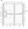
- FIG. 1 is a schematic plan view of a semiconductor device 1 according to one preferred embodiment of the present invention.
- FIG. 1 for clarification, some elements that are not exposed at the topmost surface of the semiconductor device 1 in being actually viewed planarly are shown by the solid line.
- the semiconductor device 1 is a semiconductor device that employs SiC and that is formed in, for example, a quadrangular chip shape when its topmost surface is planarly viewed from a normal direction (hereinafter, referred to simply as "when viewed planarly").
- a terminal region 3 that surrounds an active region 2 and an active region 2 is set in the semiconductor device 1.
- the active region 2 is formed in a substantially quadrangular shape when viewed planarly in an inner region of the semiconductor device 1 in the present preferred embodiment, no particular limitations are imposed on its shape.
- a guard ring (not shown) may be formed between the active region 2 and the terminal region 3 in order to improve the withstanding pressure of the semiconductor device 1.
- a gate metal 44, a source metal 43, which are examples of a control pad of the present invention, and a gate finger 5, which is an example of a finger of the present invention, are formed in the active region 2.
- a passivation film 40 is formed on the topmost surface of the semiconductor device 1. Openings 41 and 42 by which a part of the gate metal 44 and a part of the source metal 43 are exposed as a gate pad 4 and as a source pad 6, respectively, are formed in the passivation film 40.
- the gate finger 5 is wholly covered with the passivation film 40.
- the gate metal 44, the gate finger 5, and the source metal 43 are made of a metal wiring such as Al (aluminum), AlCu (aluminum-copper alloy), or Cu (copper).
- the gate metal 44 is selectively formed at a part of a peripheral edge of the active region 2 (near the boundary with the terminal region 3).
- the gate finger 5 branches and extends from the formation position of the gate pad 4 in a direction along the peripheral edge of the active region 2 and in a direction toward the inside of the active region 2.
- cell regions 7 and 45 are formed in parts partitioned by a plurality of gate fingers 5 that extend in mutually different directions with the gate metal 44 therebetween, and are formed in a region outside the gate finger 5.
- the gate metal 44 is formed in a quadrangular shape when viewed planarly, and is selectively disposed at the middle of a side 8 of the active region 2.
- the other sides except the side 8 (at which the gate metal 44 is disposed) of the active region 2 are a side 9, which is opposite to the side 8, and sides 10 and 11, which are each continuous with both ends of the sides 8 and 9.
- the gate finger 5 includes a pad peripheral portion 12 that surrounds the periphery of the gate metal 44 with a gap therebetween and first and second fingers 13 and 14 that extend from the pad peripheral portion 12 in a direction along the side 8 of the active region 2 and in a direction perpendicular to the side 8, respectively.
- the pad peripheral portion 12 is formed in a quadrangular annular shape along the periphery of the gate metal 44 when viewed planarly.
- the first finger 13 is formed as a pair along the side 8 in a direction toward the side 10 and in a direction toward the side 11 opposite to the side 10 with respect to the pad peripheral portion 12.
- the second finger 14 includes a linear main portion 15 that crosses the active region 2 up to the side 9 in a direction perpendicular to the first finger 13 and a plurality of branch portions 16 that are connected integrally with the main portion 15 and that extend from the connected places along the first finger 13.
- branch portions 16 are connected to two places, i.e., to a forward end of the main portion 15 and to a halfway portion of the main portion 15 and are formed as two pairs in total in the present preferred embodiment, no particular limitations are imposed on this number.
- cell regions 7 and 45 are defined by the first finger 13 and the second finger 14 (the main portion 15 and the branch portion 16) in the active region 2.
- one inner cell region 7 is formed at each corner of the intersection portions formed by the main portion 15 and the central branch portion 16 of the second finger 14, and hence four inner cell regions 7 in total are formed.
- an annular outer cell region 45 is formed along the peripheral edge of the active region 2 between the peripheral edge of the active region 2 and the gate finger 5.
- the source metal 43 is formed so as to cover the inner and outer cell regions 7 and 45 substantially wholly.
- Four openings 42 in total are formed in the passivation film 40 such that one of the single source pads 6 is disposed in one of the inner cell regions 7.
- a plurality of transistor cells 18 are arranged in the inner and outer cell regions 7 and 45 partitioned by the gate finger 5 (the pad peripheral portion 12, the first finger 13, and the second finger 14).
- the arrangement manner of the transistor cells 18 is not limited to the matrix manner, and may be, for example, a stripe manner or a zigzag manner.
- the planar shape of each of the transistor cells 18 is not limited to the quadrangular shape, and may be, for example, a circular, triangular, or hexagonal shape.
- the first finger 13 and the second finger 14 are respectively connected to the gate electrodes 19 disposed in a region therebelow by means of the gate contact 20.
- the gate contact 20 is formed linearly along each longitudinal direction in a finger middle with an interval from each side edge of the first and second fingers 13 and 14.
- the pattern of this symmetry is variously designable, and, for example, two built-in resistors 21 may be disposed at two corner portions, respectively, of the gate metal 44 that have an opposite-corner relationship, or two built-in resistors 21 may be disposed at two sides, respectively, of the gate metal 44 that have an opposite-side relationship so as to face each other. Additionally, for example, if the gate metal 44 is circular when viewed planarly, two built-in resistors 21 may be disposed at both ends, respectively, of the diameter of the gate metal 44, and if the gate metal 44 is triangular when viewed planarly, three built-in resistors 21 may be disposed at three corner portions, respectively, of the gate metal 44.
- each built-in resistor 21 extends from below each peripheral edge 24 of two sides of the gate metal 44 that have an opposite-side relationship in the outside direction perpendicular to these sides, and reach a part below the pad peripheral portion 12.
- Each built-in resistor 21 is formed in a quadrangular shape when viewed planarly, and has a size of, for example, 200 ⁇ m ⁇ (200 ⁇ m ⁇ 200 ⁇ m) or less. In practical use, if the size of the built-in resistor 21 is 200 ⁇ m ⁇ or less for every built-in resistor, it is possible to reduce the area of a region sacrificed for the built-in resistor among regions of a SiC epitaxial layer 28 (see FIG. 3B ), thus making it possible to realize space-saving.
- the built-in resistor 21 is disposed below the peripheral edge 24 of the gate metal 44 excluding the middle thereof, and a region above the region in which the built-in resistor 21 is disposed is covered with the passivation film 40, and, as a result, the gate pad 4 serving as a wire region of the present invention surrounded by the built-in resistors 21 is secured at the middle of the gate metal 44.
- the gate pad 4 is a region to which a bonding wire is connected.
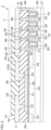
- FIG. 3A and FIG. 3B are enlarged views of a region surrounded by the alternate long and two short dashes line III of FIG. 2
- FIG. 3A is a plan view
- FIG. 3B is a cross-sectional view when the semiconductor device 1 is cut by the cutting-plane line IIIB-IIIB of FIG. 3A
- FIG. 3A and FIG. 3B for clarification, there is a case in which the reduced scale of each component differs from that in FIG. 1 and that in FIG. 2 , and, likewise, there is a case in which the reduced scale of each component differs between FIG. 3A and FIG. 3B .
- FIG. 3A and FIG. 3B for clarification, some elements that are not exposed at the topmost surface of the semiconductor device 1 when actually viewed planarly are shown by the solid line.
- the semiconductor device 1 includes a SiC substrate 27 and a SiC epitaxial layer 28.
- the SiC epitaxial layer 28 is stacked on the SiC substrate 27, and this layered structure is shown as an example of the SiC semiconductor layer of the present invention.
- the SiC substrate 27 and the SiC epitaxial layer 28 are n + type SiC and n - type SiC, respectively.
- the impurity concentration of the n + type SiC substrate 27 is, for example, 1 ⁇ 10 17 cm -3 to 1 ⁇ 10 21 cm -3 .
- the impurity concentration of the n - type SiC epitaxial layer 28 is, for example, 1 ⁇ 10 14 cm -3 to 1 ⁇ 10 17 cm -3 .
- N (nitrogen), P (phosphorus), As (arsenic), etc. can be used as n type impurities (hereinafter, same as above).
- a p - type region 34 is formed in the surface portion of the SiC epitaxial layer 28 in regions other than the inner and outer cell regions 7 and 45 in the active region 2, i.e., in regions below the gate metal 44, the gate finger 5, and the gap region 26.
- a p + type region 33 is formed in a surface portion of the p - type region 34.
- the passivation film 40 is formed on the interlayer film 36 so as to cover the gate metal 44, the gate finger 5, and the source metal 43.
- the openings 41 and 42 by which parts of the gate metal 44 and the source metal 43 are exposed are formed in the passivation film 40.
- polysilicon of which the built-in resistor 21 is made is a material in which the resistance value can be easily controlled by, for example, the implantation of impurities, and its processing has been established by a conventional semiconductor manufacturing technique. Therefore, when the built-in resistor 21 is introduced, it is also possible to avoid the complication of the structure of the semiconductor device 1 itself and of the structure of a module provided with this semiconductor device 1.
- the built-in resistor 21 is smaller in processing size than the gate electrode 19 although there is a case in which a variation in dimension and thickness is caused by a variation in processing accuracy (etching size etc.) when a semiconductor device 1 is manufactured as in the same way as in the gate electrode 19. Therefore, in the built-in resistor 21, such a variation hardly causes the occurrence of a noise.
- the transistor cell 18 is a MOSFET cell having a planar gate structure as described in the aforementioned preferred embodiment
- the transistor cell 18 may be a MOSFET cell having a trench gate structure as shown in FIG. 4 .
- the gate electrode 19 is buried in a gate trench 39 formed between the transistor cells 18 through the gate insulating film 35.
- the built-in resistor 21 is not required to be embedded in the interlayer film 36 below the gate metal 44, and, for example, a polysilicon wiring by which the gate metal 44 and the gate finger 5 are connected together may be formed on the surface of the interlayer film 36 so as to serve as a built-in resistor of the present invention.
- a material having a resistance value that is equal to or larger than that of the gate metal 44 and that of the gate finger 5 may be used as a material of the built-in resistor 21. Even if the built-in resistor 21 is a metal, it is possible to lengthen the distance between the gate metal 44 and the gate finger 5, and therefore it is possible to enlarge a resistance value obtained by totalizing the resistance value of the gate electrode 19 and the resistance value of the built-in resistor 21.
- the built-in resistor 21 may be linear along a part of the peripheral edge 24 of the gate metal 44, or may be annular along the entire periphery of the peripheral edge 24 of the gate metal 44.
- the conductivity type of each semiconductor part of the aforementioned semiconductor device 1 may be reversed.
- the p type part may be an n type
- the n type part may be a p type.
- FIG. 5 is an electric circuit diagram showing an electric circuit of a module to which the semiconductor device according to one preferred embodiment of the present invention is applied.
- a module 100 includes a plurality of semiconductor devices (chips) 101 to 104, a drain terminal 105, a source terminal 106, and a gate terminal 107.
- Each semiconductor device 101 to 104 is formed of the semiconductor device 1 shown in FIG. 1 to FIG. 3 .
- Each semiconductor device 101 to 104 may be formed of the semiconductor device shown in FIG. 4 .
- the semiconductor devices 101 to 104 are connected together in parallel.
- Each semiconductor device 101 to 104 includes a plurality of transistor cells 18 (see FIG. 2 , FIG. 3A, and FIG. 3B ) connected together in parallel and four built-in resistors 41 (see FIG. 2 , FIG. 3A, and FIG. 3B ) connected together in parallel.
- the transistor cells 18 connected together in parallel are represented as one transistor cell Tr
- the four built-in resistors 41 connected together in parallel are represented as one resistor R.
- the gate electrode of each semiconductor device 101 to 104 is connected to the gate terminal 107 of the module 100 through the built-in resistor R contained therein.
- the drain electrode of each semiconductor device 101 to 104 is connected to the drain terminal 105 of the module 100.
- the source electrode of each semiconductor device 101 to 104 is connected to the source terminal 106 of the module 100.
- this module 100 a built-in resistor R having a resistance value that is larger than the gate resistance in each semiconductor device 101 to 104 is contained in each semiconductor device 101 to 104. Therefore, in this module 100, the structure of the module becomes simpler than when an external gate resistance having a resistance value larger than the gate resistance in each semiconductor device 101 to 104 is provided in each semiconductor device 101 to 104.
Landscapes
- Semiconductor Integrated Circuits (AREA)
- Physics & Mathematics (AREA)
- Geometry (AREA)
- Metal-Oxide And Bipolar Metal-Oxide Semiconductor Integrated Circuits (AREA)
- Junction Field-Effect Transistors (AREA)
- Electrodes Of Semiconductors (AREA)
Applications Claiming Priority (5)
| Application Number | Priority Date | Filing Date | Title |
|---|---|---|---|
| JP2013246474 | 2013-11-28 | ||
| EP22199701.8A EP4141953B1 (de) | 2013-11-28 | 2014-11-26 | Halbleiteranordnung |
| PCT/JP2014/081273 WO2015080162A1 (ja) | 2013-11-28 | 2014-11-26 | 半導体装置 |
| EP14865393.4A EP3076431B1 (de) | 2013-11-28 | 2014-11-26 | Halbleiterbauelement |
| EP19215868.1A EP3644363B1 (de) | 2013-11-28 | 2014-11-26 | Halbleiterbauelement |
Related Parent Applications (4)
| Application Number | Title | Priority Date | Filing Date |
|---|---|---|---|
| EP19215868.1A Division EP3644363B1 (de) | 2013-11-28 | 2014-11-26 | Halbleiterbauelement |
| EP14865393.4A Division EP3076431B1 (de) | 2013-11-28 | 2014-11-26 | Halbleiterbauelement |
| EP22199701.8A Division EP4141953B1 (de) | 2013-11-28 | 2014-11-26 | Halbleiteranordnung |
| EP22199701.8A Division-Into EP4141953B1 (de) | 2013-11-28 | 2014-11-26 | Halbleiteranordnung |
Publications (2)
| Publication Number | Publication Date |
|---|---|
| EP4583666A2 true EP4583666A2 (de) | 2025-07-09 |
| EP4583666A3 EP4583666A3 (de) | 2025-09-03 |
Family
ID=53199101
Family Applications (4)
| Application Number | Title | Priority Date | Filing Date |
|---|---|---|---|
| EP22199701.8A Active EP4141953B1 (de) | 2013-11-28 | 2014-11-26 | Halbleiteranordnung |
| EP19215868.1A Active EP3644363B1 (de) | 2013-11-28 | 2014-11-26 | Halbleiterbauelement |
| EP14865393.4A Active EP3076431B1 (de) | 2013-11-28 | 2014-11-26 | Halbleiterbauelement |
| EP25178310.6A Pending EP4583666A3 (de) | 2013-11-28 | 2014-11-26 | Halbleiteranordnung |
Family Applications Before (3)
| Application Number | Title | Priority Date | Filing Date |
|---|---|---|---|
| EP22199701.8A Active EP4141953B1 (de) | 2013-11-28 | 2014-11-26 | Halbleiteranordnung |
| EP19215868.1A Active EP3644363B1 (de) | 2013-11-28 | 2014-11-26 | Halbleiterbauelement |
| EP14865393.4A Active EP3076431B1 (de) | 2013-11-28 | 2014-11-26 | Halbleiterbauelement |
Country Status (5)
| Country | Link |
|---|---|
| US (6) | US9917102B2 (de) |
| EP (4) | EP4141953B1 (de) |
| JP (6) | JP6595915B2 (de) |
| CN (2) | CN110634825B (de) |
| WO (1) | WO2015080162A1 (de) |
Families Citing this family (28)
| Publication number | Priority date | Publication date | Assignee | Title |
|---|---|---|---|---|
| EP4141953B1 (de) | 2013-11-28 | 2025-07-02 | Rohm Co., Ltd. | Halbleiteranordnung |
| DE102015120747B4 (de) * | 2015-11-30 | 2020-10-22 | Infineon Technologies Austria Ag | Transistorbauelement mit erhöhter gate-drain-kapazität |
| JP6941502B2 (ja) * | 2016-09-30 | 2021-09-29 | ローム株式会社 | 半導体装置および半導体パッケージ |
| US10692863B2 (en) | 2016-09-30 | 2020-06-23 | Rohm Co., Ltd. | Semiconductor device and semiconductor package |
| US10403623B2 (en) * | 2017-07-06 | 2019-09-03 | General Electric Company | Gate networks having positive temperature coefficients of resistance (PTC) for semiconductor power conversion devices |
| US10665713B2 (en) * | 2017-09-28 | 2020-05-26 | Mitsubishi Electric Corporation | Silicon carbide semiconductor device |
| JP6958474B2 (ja) * | 2017-09-28 | 2021-11-02 | 三菱電機株式会社 | 炭化珪素半導体装置 |
| EP3531457B1 (de) * | 2018-02-26 | 2022-07-20 | Infineon Technologies Austria AG | Transistorvorrichtung mit gate-widerstand |
| JP7172317B2 (ja) | 2018-09-11 | 2022-11-16 | 富士電機株式会社 | 半導体装置 |
| WO2020090925A1 (ja) * | 2018-11-02 | 2020-05-07 | ローム株式会社 | 半導体ユニット、半導体装置、バッテリユニット、及び車両 |
| JP7139232B2 (ja) * | 2018-12-07 | 2022-09-20 | ルネサスエレクトロニクス株式会社 | 半導体装置及び半導体装置の製造方法 |
| JP7234713B2 (ja) * | 2019-03-14 | 2023-03-08 | 富士電機株式会社 | 半導体装置 |
| EP3716340A1 (de) * | 2019-03-25 | 2020-09-30 | Infineon Technologies Austria AG | Transistorvorrichtung |
| FR3096832B1 (fr) * | 2019-05-28 | 2022-05-13 | St Microelectronics Rousset | Structure de transistor |
| CN111403341B (zh) * | 2020-03-28 | 2023-03-28 | 电子科技大学 | 降低窄控制栅结构栅电阻的金属布线方法 |
| US12484286B2 (en) | 2020-03-30 | 2025-11-25 | Sumitomo Electric Industries, Ltd. | Transistor and semiconductor device |
| CN119050153A (zh) * | 2020-09-17 | 2024-11-29 | 罗姆股份有限公司 | 半导体装置 |
| JP7471974B2 (ja) | 2020-09-18 | 2024-04-22 | 株式会社東芝 | 半導体装置 |
| US11664436B2 (en) | 2021-03-01 | 2023-05-30 | Wolfspeed, Inc. | Semiconductor devices having gate resistors with low variation in resistance values |
| CN116998020A (zh) * | 2021-03-22 | 2023-11-03 | 罗姆股份有限公司 | 半导体装置 |
| TWI844493B (zh) * | 2021-03-29 | 2024-06-01 | 日商新唐科技日本股份有限公司 | 半導體裝置 |
| US11810912B2 (en) | 2021-07-22 | 2023-11-07 | Wolfspeed, Inc. | Semiconductor devices having asymmetric integrated gate resistors for balanced turn-on/turn-off behavior |
| US20230023195A1 (en) * | 2021-07-22 | 2023-01-26 | Wolfspeed, Inc. | Semiconductor devices having asymmetric integrated lumped gate resistors for balanced turn-on/turn-off behavior and/or multiple spaced-apart lumped gate resistors for improved power handling |
| JP7658827B2 (ja) * | 2021-07-26 | 2025-04-08 | 三菱電機株式会社 | 半導体装置及びその製造方法 |
| IT202100024752A1 (it) * | 2021-09-28 | 2023-03-28 | St Microelectronics Srl | Dispositivo di potenza in carburo di silicio con resistenza integrata e relativo procedimento di fabbricazione |
| US20230120729A1 (en) * | 2021-10-15 | 2023-04-20 | Wolfspeed, Inc. | Power semiconductor devices including multiple gate bond pads |
| US20230155013A1 (en) * | 2021-11-18 | 2023-05-18 | Renesas Electronics Corporation | Semiconductor device |
| WO2025142732A1 (ja) * | 2023-12-28 | 2025-07-03 | ローム株式会社 | 半導体装置 |
Citations (2)
| Publication number | Priority date | Publication date | Assignee | Title |
|---|---|---|---|---|
| JP2010238885A (ja) | 2009-03-31 | 2010-10-21 | Renesas Electronics Corp | 半導体装置とその製造方法 |
| JP2013246474A (ja) | 2012-05-23 | 2013-12-09 | Nippon Telegr & Teleph Corp <Ntt> | 中継サーバおよび代理アクセス方法 |
Family Cites Families (47)
| Publication number | Priority date | Publication date | Assignee | Title |
|---|---|---|---|---|
| JPH0758781B2 (ja) * | 1985-10-24 | 1995-06-21 | 三菱電機株式会社 | 電界効果型半導体装置 |
| JPS62224074A (ja) * | 1986-03-26 | 1987-10-02 | Hitachi Ltd | 絶縁ゲ−ト半導体装置 |
| US4920388A (en) * | 1987-02-17 | 1990-04-24 | Siliconix Incorporated | Power transistor with integrated gate resistor |
| JPS6418267A (en) * | 1987-07-13 | 1989-01-23 | Fuji Electric Co Ltd | Semiconductor device |
| JPH01305576A (ja) * | 1988-06-03 | 1989-12-08 | Fujitsu Ltd | Mis型電界効果トランジスタ |
| JPH04186872A (ja) * | 1990-11-21 | 1992-07-03 | Nec Corp | 縦型mos電界効果トランジスタの製造方法 |
| DE19512799C2 (de) * | 1995-04-05 | 1998-11-12 | Siemens Ag | Durch Feldeffekt steuerbares Halbleiterbauelement |
| JPH09219493A (ja) * | 1996-02-08 | 1997-08-19 | Hitachi Ltd | 抵抗素子及びこの製造方法並びにそれが集積された半導体装置 |
| US6236088B1 (en) * | 1997-06-30 | 2001-05-22 | Intersil Corporation | Semiconductor device gate structure for thermal overload protection |
| JPH11312786A (ja) * | 1998-04-30 | 1999-11-09 | Hitachi Ltd | 半導体集積回路 |
| JP2000294770A (ja) | 1999-04-09 | 2000-10-20 | Rohm Co Ltd | 半導体装置 |
| JP3505461B2 (ja) * | 2000-03-03 | 2004-03-08 | 三洋電機株式会社 | 絶縁ゲート型半導体装置 |
| JP4032622B2 (ja) * | 2000-09-06 | 2008-01-16 | 株式会社日立製作所 | 半導体素子及びこれを用いた半導体装置と変換器 |
| JP3881840B2 (ja) * | 2000-11-14 | 2007-02-14 | 独立行政法人産業技術総合研究所 | 半導体装置 |
| JP2002246598A (ja) * | 2001-02-15 | 2002-08-30 | Nec Yamagata Ltd | 半導体装置及びその製造方法 |
| JP4846106B2 (ja) * | 2001-02-16 | 2011-12-28 | 三菱電機株式会社 | 電界効果型半導体装置及びその製造方法 |
| JP2002353452A (ja) * | 2001-05-25 | 2002-12-06 | Toshiba Corp | 電力用半導体素子 |
| JP2002368218A (ja) | 2001-06-08 | 2002-12-20 | Sanyo Electric Co Ltd | 絶縁ゲート型半導体装置 |
| JP2003197914A (ja) * | 2001-12-28 | 2003-07-11 | Fuji Electric Co Ltd | 半導体装置 |
| KR100446293B1 (ko) * | 2002-01-07 | 2004-09-01 | 삼성전자주식회사 | 저항체를 포함하는 반도체 소자 제조 방법 |
| JP2004172448A (ja) | 2002-11-21 | 2004-06-17 | Renesas Technology Corp | 半導体装置 |
| JP2005228851A (ja) * | 2004-02-12 | 2005-08-25 | Mitsubishi Electric Corp | Igbtモジュール |
| KR100629357B1 (ko) * | 2004-11-29 | 2006-09-29 | 삼성전자주식회사 | 퓨즈 및 부하저항을 갖는 낸드 플래시메모리소자 형성방법 |
| KR20070013132A (ko) * | 2005-07-25 | 2007-01-30 | 삼성전자주식회사 | 박막트랜지스터 기판과 박막트랜지스터 기판의 제조방법 |
| JP2007042817A (ja) | 2005-08-02 | 2007-02-15 | Sanyo Electric Co Ltd | 絶縁ゲート型半導体装置およびその製造方法 |
| US20070176295A1 (en) * | 2006-02-01 | 2007-08-02 | International Business Machines Corporation | Contact via scheme with staggered vias |
| JP5048273B2 (ja) * | 2006-05-10 | 2012-10-17 | オンセミコンダクター・トレーディング・リミテッド | 絶縁ゲート型半導体装置 |
| US7443225B2 (en) * | 2006-06-30 | 2008-10-28 | Alpha & Omega Semiconductor, Ltd. | Thermally stable semiconductor power device |
| EP2041791A1 (de) * | 2006-07-03 | 2009-04-01 | Freescale Semiconductor, Inc. | Vorrichtung zum schutz vor elektrostatischer entladung und verfahren dafür |
| JP2008270492A (ja) | 2007-04-19 | 2008-11-06 | Sanyo Electric Co Ltd | 絶縁ゲート型半導体装置 |
| JP5132977B2 (ja) | 2007-04-26 | 2013-01-30 | ルネサスエレクトロニクス株式会社 | 半導体装置およびその製造方法 |
| JP5138274B2 (ja) * | 2007-05-25 | 2013-02-06 | 三菱電機株式会社 | 半導体装置 |
| WO2009013886A1 (ja) * | 2007-07-20 | 2009-01-29 | Panasonic Corporation | 炭化珪素半導体装置およびその製造方法 |
| JP4442698B2 (ja) * | 2007-07-25 | 2010-03-31 | 三菱電機株式会社 | 炭化珪素半導体装置の製造方法 |
| JP2009295867A (ja) * | 2008-06-06 | 2009-12-17 | Rohm Co Ltd | 半導体装置 |
| JP2010016103A (ja) * | 2008-07-02 | 2010-01-21 | Panasonic Corp | 半導体装置 |
| JP2010087124A (ja) | 2008-09-30 | 2010-04-15 | Sanyo Electric Co Ltd | 絶縁ゲート型半導体装置 |
| JP2010153636A (ja) | 2008-12-25 | 2010-07-08 | Sanyo Electric Co Ltd | 絶縁ゲート型半導体装置 |
| US8324686B2 (en) * | 2009-01-16 | 2012-12-04 | Infineon Technologies Austria Ag | Semiconductor device and method for manufacturing |
| JP5476028B2 (ja) * | 2009-04-17 | 2014-04-23 | 株式会社日立製作所 | パワー半導体スイッチング素子のゲート駆動回路及びインバータ回路 |
| US8053809B2 (en) * | 2009-05-26 | 2011-11-08 | International Business Machines Corporation | Device including high-K metal gate finfet and resistive structure and method of forming thereof |
| JP4962664B2 (ja) * | 2009-10-14 | 2012-06-27 | 三菱電機株式会社 | 電力用半導体装置とその製造方法、ならびにパワーモジュール |
| JP4962665B2 (ja) | 2010-04-06 | 2012-06-27 | 三菱電機株式会社 | 電力用半導体装置およびその製造方法、ならびにパワーモジュール |
| JP5755533B2 (ja) | 2011-08-26 | 2015-07-29 | ルネサスエレクトロニクス株式会社 | 半導体装置 |
| CN105324833B (zh) * | 2013-06-14 | 2018-02-02 | 新电元工业株式会社 | 半导体装置的制造方法以及半导体装置 |
| CN103367164B (zh) * | 2013-06-26 | 2015-11-11 | 株洲南车时代电气股份有限公司 | 一种栅极电极及其制备方法 |
| EP4141953B1 (de) | 2013-11-28 | 2025-07-02 | Rohm Co., Ltd. | Halbleiteranordnung |
-
2014
- 2014-11-26 EP EP22199701.8A patent/EP4141953B1/de active Active
- 2014-11-26 WO PCT/JP2014/081273 patent/WO2015080162A1/ja not_active Ceased
- 2014-11-26 CN CN201910879948.1A patent/CN110634825B/zh active Active
- 2014-11-26 CN CN201480065081.1A patent/CN106415837B/zh active Active
- 2014-11-26 JP JP2015550968A patent/JP6595915B2/ja active Active
- 2014-11-26 EP EP19215868.1A patent/EP3644363B1/de active Active
- 2014-11-26 US US15/039,725 patent/US9917102B2/en active Active
- 2014-11-26 EP EP14865393.4A patent/EP3076431B1/de active Active
- 2014-11-26 EP EP25178310.6A patent/EP4583666A3/de active Pending
-
2018
- 2018-01-30 US US15/883,690 patent/US10438971B2/en active Active
-
2019
- 2019-07-29 JP JP2019138919A patent/JP2019197920A/ja active Pending
- 2019-08-29 US US16/555,843 patent/US10886300B2/en active Active
-
2020
- 2020-12-02 US US17/109,676 patent/US11367738B2/en active Active
-
2021
- 2021-09-21 JP JP2021152878A patent/JP7413329B2/ja active Active
-
2022
- 2022-05-19 US US17/748,633 patent/US11908868B2/en active Active
-
2023
- 2023-12-27 JP JP2023221217A patent/JP7618775B2/ja active Active
-
2024
- 2024-01-17 US US18/414,540 patent/US20240153955A1/en active Pending
-
2025
- 2025-01-08 JP JP2025003111A patent/JP2025036776A/ja active Pending
- 2025-05-28 JP JP2025089286A patent/JP7804817B2/ja active Active
Patent Citations (2)
| Publication number | Priority date | Publication date | Assignee | Title |
|---|---|---|---|---|
| JP2010238885A (ja) | 2009-03-31 | 2010-10-21 | Renesas Electronics Corp | 半導体装置とその製造方法 |
| JP2013246474A (ja) | 2012-05-23 | 2013-12-09 | Nippon Telegr & Teleph Corp <Ntt> | 中継サーバおよび代理アクセス方法 |
Also Published As
Similar Documents
| Publication | Publication Date | Title |
|---|---|---|
| US11908868B2 (en) | Semiconductor device | |
| US20240332367A1 (en) | SiC SEMICONDUCTOR DEVICE WITH INSULATING FILM AND ORGANIC INSULATING LAYER | |
| CN100576542C (zh) | 绝缘栅型半导体装置 | |
| US9431491B2 (en) | Semiconductor device and method of manufacturing the same | |
| JP6941502B2 (ja) | 半導体装置および半導体パッケージ | |
| JP2020074382A (ja) | 半導体装置 | |
| CN118633167A (zh) | 半导体装置 | |
| JP2023085505A (ja) | 半導体装置 | |
| JP7442750B1 (ja) | 半導体装置 | |
| CN223943088U (zh) | 半导体装置 | |
| WO2024018715A1 (ja) | 半導体装置 |
Legal Events
| Date | Code | Title | Description |
|---|---|---|---|
| PUAI | Public reference made under article 153(3) epc to a published international application that has entered the european phase |
Free format text: ORIGINAL CODE: 0009012 |
|
| STAA | Information on the status of an ep patent application or granted ep patent |
Free format text: STATUS: REQUEST FOR EXAMINATION WAS MADE |
|
| 17P | Request for examination filed |
Effective date: 20250522 |
|
| AC | Divisional application: reference to earlier application |
Ref document number: 3076431 Country of ref document: EP Kind code of ref document: P Ref document number: 3644363 Country of ref document: EP Kind code of ref document: P Ref document number: 4141953 Country of ref document: EP Kind code of ref document: P |
|
| AK | Designated contracting states |
Kind code of ref document: A2 Designated state(s): AL AT BE BG CH CY CZ DE DK EE ES FI FR GB GR HR HU IE IS IT LI LT LU LV MC MK MT NL NO PL PT RO RS SE SI SK SM TR |
|
| PUAL | Search report despatched |
Free format text: ORIGINAL CODE: 0009013 |
|
| AK | Designated contracting states |
Kind code of ref document: A3 Designated state(s): AL AT BE BG CH CY CZ DE DK EE ES FI FR GB GR HR HU IE IS IT LI LT LU LV MC MK MT NL NO PL PT RO RS SE SI SK SM TR |
|
| RIC1 | Information provided on ipc code assigned before grant |
Ipc: H10D 84/00 20250101AFI20250731BHEP Ipc: H10D 30/66 20250101ALI20250731BHEP Ipc: H10D 62/832 20250101ALI20250731BHEP Ipc: H10D 64/27 20250101ALI20250731BHEP |