【0001】
【発明の属する技術分野】
本発明は、低い比誘電率を与えるポリベンゾオキサゾール、その前駆体、これを用いた感光性樹脂組成物及びこれを用いた電子部品に関する。
【0002】
【従来の技術】
従来、半導体素子の表面保護膜又は層間絶縁膜としては、耐熱性、機械特性及び電気特性に優れ、また、膜形成が容易であり、表面を平坦化できる等の利点から、ポリイミドが幅広く使用されている。
ポリイミドを表面保護膜又は層間絶縁膜として使用する場合、スルーホール等の形成工程は、主にポジ型のフォトレジストを用いるエッチングプロセスによって行われている。しかし、工程にはフォトレジストの塗布や剥離が含まれ、煩雑であるという問題がある。そこで作業工程の合理化を目的に感光性を兼ね備えた耐熱性材料の検討がなされてきた。
【0003】
感光性ポリイミド組成物に関しては、1.エステル結合により感光基を導入したポリイミド前駆体組成物(特公昭52−30207号公報等)、2.ポリアミド酸に化学線の照射により2量化又は重合可能な炭素−炭素二重結合及びアミノ基と芳香族ビスアジドを含む化合物を添加した組成物(特公平3−36861号公報等)などが知られ、用いられている。
【0004】
感光性ポリイミド組成物の使用に際しては、通常、溶液状態で基板上に塗布後乾燥し、マスクを介して活性光線を照射し、露光部を現像液で除去し、パターンを形成する。
上記1及び2の組成物は、現像液に有機溶剤を使用するネガ型である。有機溶剤の現像液は、廃液処理の際の環境への負荷が大きく、近年環境への配慮から、廃現像液の処理の容易な水性現像液で現像可能な感光性耐熱材料が求められている。また、ポジ型のフォトレジストを用いるエッチングプロセスからネガ型の感光性ポリイミドに切り替えるためには、露光装置のマスクや現像設備の変更が必要となる。上記1、2の組成物は以上述べたような問題点がある。
【0005】
一方、ポジ型感光性ポリイミドとしては、3.o−ニトロベンジル基をエステル結合により導入したポリイミド前駆体(特開昭60−37550号公報)、 4.フェノール性水酸基を含むポリアミド酸エステルとo−ジアゾキノン化合物を含む組成物(特開平4−204945号公報)等が知られている。また、ポジ型の耐熱性材料として、ポリイミドと同等の、耐熱性、機械特性、電気特性を有するポリベンズオキサゾールを使用した感光剤材料、5.ポリベンズオキサゾール前駆体とo−ジアゾキノン化合物を含む組成物(特開昭64−6947号公報、特開平9−302221号公報等)も知られている。
【0006】
しかし、上記3は感光する波長が主に300nm以下であるため、感度が低く、特に最近使用されているi線ステッパ(365nmの単波長光)等では使用が困難であるという問題がある。上記4、5の組成物は、上記3の前駆体より感度はよいが、十分ではないという問題がある。このように、十分な感度を有するポジ型感光性耐熱材料は得られていないのが現状である。
【0007】
【発明が解決しようとする課題】
本発明は、ポリベンゾオキサゾール前駆体における良好なi線透過性とポリベンゾオキサゾール化後の低い比誘電率及び高耐熱性を有するポリベンゾオキサゾール前駆体及びこれを用いた感光性樹脂組成物を提供するものである。
また本発明は、低い比誘電率と高耐熱性となるポリベンゾオキサゾールを提供するものである。
さらに本発明は、ポリベンゾオキサゾール膜形成後の比誘電率が究めて小さく、高耐熱性を有する膜を使用した信頼性に優れる電子部品を提供するものである。
【0008】
【課題を解決するための手段】
本発明は一般式(1)
【化4】
(式中、Xは2価の有機基であり、Yは4価の有機基であり、XとYの両方または一方はアダマンタン構造を主鎖に有する)で表される繰り返し単位を有するポリベンゾオキサゾール前駆体に関する。
【0009】
また本発明は、前記前駆体が、膜厚10μm当りのi線透過率が10%以上であり、このポリベンゾオキサゾール前駆体を脱水閉環して形成されたポリベンゾオキサゾール膜の比誘電率が2.8未満となるものであるポリベンゾオキサゾール前駆体に関する。
また本発明は、前記一般式(1)が、一般式(2)
【化5】
(式中、Yは4価の有機基である)であるポリベンゾオキサゾール前駆体に関する。
【0010】
また本発明は、前記のポリベンゾオキサゾール前駆体と感光剤を含有してなる感光性樹脂組成物に関する。
また本発明は、一般式(3)
【化6】
(式中、Xは2価の有機基であり、Yは4価の有機基であり、XとYの両方または一方が脂環構造を主鎖に有する)で表される繰り返し単位を有するポリベンゾオキサゾール前駆体であり、その膜厚10μm当りのi線透過率が10%以上であり、このポリベンゾオキサゾール前駆体を脱水閉環して形成されたポリベンゾオキサゾール膜の比誘電率が2.8未満となるポリベンゾオキサゾール前駆体と感光剤を含有してなる感光性樹脂組成物に関する。
【0011】
また本発明は、前記感光剤が、光により酸を発生する化合物である感光性樹脂組成物に関する。
また本発明は、前記のポリベンゾオキサゾール前駆体を脱水閉環して形成されるポリベンゾオキサゾールに関する。
さらに本発明は、前記のポリベンゾオキサゾールの膜を表面保護膜又は層間絶縁膜として有してなる電子部品に関する。
【0012】
【発明の実施の形態】
本発明のポリベンゾオキサゾール前駆体は、前記一般式(1)で表される繰り返し単位を有する。一般式(1)においては、X又はYのいずれかにアダマンタン構造を有することが必要であるが、前駆体における高い光透過性を発現し、ポリベンゾオキサゾール膜の低い比誘電率と高い耐熱性を両立するためには、特にXがアダマンタン構造を有することが好ましい。この場合Yは、前駆体における光透過性とポリベンゾオキサゾール膜の比誘電率や耐熱性を低下させない構造であればよく、例えば非連続芳香環構造(芳香環同士が2価の基を介して結合している構造)や芳香環が連続している場合(芳香環同士が直接共有結合している構造)でも芳香環がねじれる構造や、フッ素原子を含有する構造などが好ましい。
【0013】
本発明のポリベンゾオキサゾール前駆体は、そのプリベイク膜厚10μm当りのi線透過率は10%であることが好ましく、30%以上であることがより好ましく、50〜100%であることがさらに好ましい。透過率が低い場合はパターン性(感度や解像度)が低下する。
i線透過率の測定においては、プリベイク膜厚はポリベンゾオキサゾール前駆体溶液の濃度や塗布時のスピン速度などで調整できる。具体的には厚さ0.2mmのガラス板上にポリベンゾオキサゾール前駆体溶液をスピンコートで塗布後、ホットプレート上で溶媒を揮発させ、プリベイク膜を作製する。プリベイク条件は80℃×100秒、95℃×100秒であることが好ましい。後述する実施例ではこの方法で作成した。また、プリベイク膜厚の測定は触針式表面粗さ計により行うことができる。i線透過率の測定は、分光光度計により行うことができる。
【0014】
また本発明のポリベンゾオキサゾール前駆体は、比誘電率が2.8未満とすることが好ましい。2.8以上になると配線部における信号遅延が顕在化するという欠点がある。比誘電率は次のようにして測定される。即ちポリベンゾオキサゾール前駆体溶液をスピンナーにより低抵抗シリコンウェハ上に回転塗布した後、350℃で1時間加熱硬化して得た硬化膜(膜厚10μm)上に、真空蒸着法で5mmφのアルミ電極を形成する。次にインピーダンスアナライザを用いてアルミ電極−低抵抗シリコンウェハ間の電荷容量を測定し、得られた値から比誘電率の算出ができる。
【0015】
なお、上記のi線透過率を有するポリベンゾオキサゾール前駆体は、例えば、脂環式構造を導入することにより調整できる。一般に脂環式構造は熱分解温度が低い欠点があるが、本発明のポリベンゾオキサゾール前駆体におけるアダマンタン構造は脂環構造を橋架けする構造となっているため、i線透過性と耐熱性を両立できる。
【0016】
本発明において、一般式(1)で表される繰り返し単位を有するポリベンゾオキサゾール前駆体は、一般的にジカルボン酸誘導体とヒドロキシ基含有ジアミン類とから合成できる。具体的には、ジカルボン酸誘導体をジハライド誘導体に変換後、前記ジアミン類との反応を行うことにより合成できる。ジハライド誘導体としては、ジクロリド誘導体が好ましい。
【0017】
ジクロリド誘導体は、ジカルボン酸誘導体にハロゲン化剤を作用させて合成することができる。ハロゲン化剤としては通常のカルボン酸の酸クロ化反応に使用される塩化チオニル、塩化ホスホリル、オキシ塩化リン、五塩化リン等が使用できる。
【0018】
ジクロリド誘導体を合成する方法としては、ジカルボン酸誘導体と上記ハロゲン化剤を溶媒中で反応させるか、過剰のハロゲン化剤中で反応を行った後、過剰分を留去する方法で合成できる。反応溶媒としは、N−メチル−2−ピロリドン、N−メチル−2−ピリドン、N,N−ジメチルアセトアミド、N,N−ジメチルホルムアミド、トルエン、ベンゼン等が使用できる。
【0019】
これらのハロゲン化剤の使用量は、溶媒中で反応させる場合は、ジカルボン酸誘導体1モルに対して、1.5〜3.0モルが好ましく、1.7〜2.5モルがより好ましく、ハロゲン化剤中で反応させる場合は、4.0〜50モルが好ましく、5.0〜20モルがより好ましい。反応温度は、−10〜70℃が好ましく、0〜20℃がより好ましい。
【0020】
ジクロリド誘導体とジアミン類との反応は、脱ハロゲン化水素剤の存在下に、有機溶媒中で行うことが好ましい。脱ハロゲン化水素剤としては、通常、ピリジン、トリエチルアミン等の有機塩基が使用される。また、有機溶媒としは、N−メチル−2−ピロリドン、N−メチル−2−ピリドン、N,N−ジメチルアセトアミド、N,N−ジメチルホルムアミド等が使用できる。反応温度は、−10〜30℃が好ましく、0〜20℃がより好ましい。
【0021】
ここで、一般式(1)において、Yで表される4価の有機基とは、一般に、ジカルボン酸と反応してポリアミド構造を形成する、2個のヒドロキシ基がそれぞれアミノ基のオルト位に位置した構造を有するジアミンの残基である。具体的には、4価のアダマンタン構造や他の脂環式構造を有する芳香族基が好ましい。炭素原子数としては6〜40のものが好ましく、炭素原子数6〜40の4価の芳香族基がより好ましい。4価の芳香族基としては、4個の結合部位がいずれも芳香環上に存在するものが好ましい。
【0022】
アダマンタン構造を主鎖に有する、このようなジアミン類としては、
【化7】
(各式中Zは、O、CO、COOのいずれかを示す。)が挙げられる。
【0023】
また、その他の脂環構造を有するジアミン類としては、
【化8】
(各式中Zは、O、CO、COOのいずれかを示す。)で示されるものが挙げられる。
【0024】
その他、3,3’−ジアミノ−4,4’−ジヒドロキシビフェニル、4,4’−ジアミノ−3,3’−ジヒドロキシビフェニル、ビス(3−アミノ−4−ヒドロキシフェニル)プロパン、ビス(4−アミノ−3−ヒドロキシフェニル)プロパン、ビス(3−アミノ−4−ヒドロキシフェニル)スルホン、ビス(4−アミノ−3−ヒドロキシフェニル)スルホン、2,2−ビス(3−アミノ−4−ヒドロキシフェニル)−1,1,1,3,3,3−ヘキサフルオロプロパン、2,2−ビス(4−アミノ−3−ヒドロキシフェニル)−1,1,1,3,3,3−ヘキサフルオロプロパン等の脂環構造を有しない、芳香族系のジアミン類が挙げられる。さらに、脂環式のジアミンや脂肪族系のジアミンを本発明の効果が損なわれない程度に併用することも可能である。
これらの化合物は、単独で又は2種以上を組み合わせて用いることができる。
【0025】
また一般式(1)において、Xで表される2価の有機基とは、ジアミンと反応してポリアミド構造を形成する、ジカルボン酸の残基であり、アダマンタン構造を有する2価の脂環式構造が好ましく、炭素原子数としては10〜40のものが好ましく、炭素原子数10〜40の2価の脂環式構造がより好ましい。より好ましい2価の脂環式構造としては、2個の結合部位がいずれもアダマンタン構造上に存在するものである。
【0026】
このようなアダマンタン構造を有するジカルボン酸としては、
【化9】
(各式中Zは、O、CO、COOのいずれかを示す。)などが挙げられる。
これらの化合物は、単独で又は2種以上を組み合わせて使用することができる。
【0027】
また、一般式(1)において、Yがアダマンタン構造を有する場合や、上記アダマンタン構造を有するジカルボン酸との併用として、好ましくはポリベンゾオキサゾール前駆体膜のi線透過率を著しく低下させない程度に、芳香族ジカルボン酸や他の脂肪族ジカルボン酸を共重合させても良い。
このような芳香族ジカルボン酸としては、イソフタル酸、テレフタル酸、2,2−ビス(4−カルボキシフェニル)−1,1,1,3,3,3−ヘキサフルオロプロパン、4,4’−ジカルボキシビフェニル、4,4’−ジカルボキシジフェニルエーテル、4,4’−ジカルボキシテトラフェニルシラン、ビス(4−カルボキシフェニル)スルホン、2,2−ビス(p−カルボキシフェニル)プロパン、5−tert−ブチルイソフタル酸、5−ブロモイソフタル酸、5−フルオロイソフタル酸、5−クロロイソフタル酸、2,6−ナフタレンジカルボン酸等の芳香族系ジカルボン酸、1,2−シクロブタンジカルボン酸、1,4−シクロヘキサンジカルボン酸、1,3−シクロペンタンジカルボン酸、シュウ酸、マロン酸、コハク酸等の脂肪族系ジカルボン酸などが挙げられる。
【0028】
また、他の脂環式構造を有するジカルボン酸としては、
【化10】
(各式中Rは、CH3、C2H5等のアルキル基、C6H5等のアリール基)などが挙げられる。
これらの化合物を、単独で又は2種以上を組み合わせて使用することができる。
【0029】
本発明のポリベンゾオキサゾール前駆体の分子量は特に制限されないが、一般に重量平均分子量で、5,000〜500,000が好ましく、10,000〜50,000がより好ましい。なお、重量平均分子量は、ゲルパーミエーションクロマトグラフィー法により測定し、標準ポリスチレン検量線を用いて換算することができる。
【0030】
本発明の感光性樹脂組成物は、前記のアダマンタン構造を有するポリベンゾオキサゾール前駆体を使用することが特性上好ましいが、それ以外の、前記一般式(3)で表される繰り返し単位を有するポリベンゾオキサゾール前駆体(即ち、繰り返し単位のXとYの両方または一方が脂環構造を主鎖に有するもの)であり、その膜厚10μm当りのi線透過率が10%以上であり、このポリベンゾオキサゾール前駆体を脱水閉環して形成されたポリベンゾオキサゾール膜の比誘電率が2.8未満となるポリベンゾオキサゾール前駆体を用いることもできる。
【0031】
本発明の感光性樹脂組成物は、前記ポリベンゾオキサゾール前駆体とともに感光剤を含む。感光剤とは、光に感応して、その組成物から形成された膜の現像液に対する溶解性を変化させる機能を有するものである。感光剤には特に制限はないが、一般にポジ型の感光性樹脂組成物においては光により酸を発生する化合物が使用される。これは酸を発生させ、光の照射部のアルカリ水溶液への可溶性を増大させる機能を有するものである。その種類としては、o−キノンジアジド化合物、アリールジアゾニウム塩、ジアリールヨードニウム塩、トリアリールスルホニウム塩などが挙げられ、特に制限はないが、o−キノンジアジド化合物が感度が高く好ましいものとして挙げられる。
【0032】
o−キノンジアジド化合物は、例えば、o−キノンジアジドスルホニルクロリド類とヒドロキシ化合物、アミノ化合物などとを脱塩酸剤の存在下で縮合反応させることで得られる。
前記o−キノンジアジドスルホニルクロリド類としては、例えば、ベンゾキノン−1,2−ジアジド−4−スルホニルクロリド、ナフトキノン−1,2−ジアジド−5−スルホニルクロリド、ナフトキノン−1,2−ジアジド−4−スルホニルクロリド等が使用できる。
【0033】
前記ヒドロキシ化合物としては、例えば、ヒドロキノン、レゾルシノール、ピロガロール、ビスフェノールA、ビス(4−ヒドロキシフェニル)メタン、2,2−ビス(4−ヒドロキシフェニル)ヘキサフルオロプロパン、2,3,4−トリヒドロキシベンゾフェノン、2,3,4,4’−テトラヒドロキシベンゾフェノン、2,2’,4,4’−テトラヒドロキシベンゾフェノン、2,3,4, 2’,3’−ペンタヒドロキシベンゾフェノン、2,3,4,3’,4’,5’−ヘキサヒドロキシベンゾフェノン、ビス(2,3,4−トリヒドロキシフェニル)メタン、ビス(2,3,4−トリヒドロキシフェニル)プロパン、4b,5,9b,10−テトラヒドロ−1,3,6,8−テトラヒドロキシ−5,10−ジメチルインデノ[2,1−a]インデン、トリス(4−ヒドロキシフェニル)メタン、トリス(4−ヒドロキシフェニル)エタンなどが使用できる。
【0034】
アミノ化合物としては、例えば、p−フェニレンジアミン、m−フェニレンジアミン、4,4’−ジアミノジフェニルエーテル、4,4’−ジアミノジフェニルメタン、4,4’−ジアミノジフェニルスルホン、4,4’−ジアミノジフェニルスルフィド、o−アミノフェノール、m−アミノフェノール、p−アミノフェノール、3,3’−ジアミノ−4,4’−ジヒドロキシビフェニル、4,4’−ジアミノ−3,3’−ジヒドロキシビフェニル、ビス(3−アミノ−4−ヒドロキシフェニル)プロパン、ビス(4−アミノ−3−ヒドロキシフェニル)プロパン、ビス(3−アミノ−4−ヒドロキシフェニル)スルホン、ビス(4−アミノ−3−ヒドロキシフェニル)スルホン、ビス(3−アミノ−4−ヒドロキシフェニル)ヘキサフルオロプロパン、ビス(4−アミノ−3−ヒドロキシフェニル)ヘキサフルオロプロパンなどが使用できる。
【0035】
o−キノンジアジドスルホニルクロリドとヒドロキシ化合物及び/又はアミノ化合物とは、o−キノンジアジドスルホニルクロリド1モルに対して、ヒドロキシ基とアミノ基の合計が0.5〜1モルになるように配合されることが好ましい。脱塩酸剤とo−キノンジアジドスルホニルクロリドの好ましい割合は、0.95/1〜1/0.95の範囲である。好ましい反応温度は0〜40℃、好ましい反応時間は1〜10時間とされる。
【0036】
反応溶媒としては、ジオキサン、アセトン、メチルエチルケトン、テトラヒドロフラン、ジエチルエーテル、N−メチルピロリドン等の溶媒が用いられる。
脱塩酸剤としては、炭酸ナトリウム、水酸化ナトリウム、炭酸水素ナトリウム、炭酸カリウム、水酸化カリウム、トリメチルアミン、トリエチルアミン、ピリジンなどがあげられる。
【0037】
感光剤の量は、特に制限されないが、感度や残膜率の点から前記ポリベンゾオキサゾール前駆体100重量部に対して、1〜50重量部が好ましい。
本発明の感光性樹脂組成物は、前記ポリベンゾオキサゾール前駆体、感光剤成分を必須成分とし、これを溶剤に溶解して得ることができる。
【0038】
溶剤としては、例えば、N−メチル−2−ピロリドン、N,N−ジメチルホルムアミド、N,N−ジメチルアセトアミド、ジメチルスルホキシド、ヘキサメチルホスホリルアミド、テトラメチレンスルホン、γ−ブチロラクトン等の非プロトン性極性溶剤が好ましく、これらを単独で又は2種以上併用して用いられる。
【0039】
また、塗布性向上のため、ジエチルケトン、ジイソブチルケトン、メチルアミルケトン、乳酸エチル、プロピレングリコールモノメチルエーテルアセテート等の溶剤を併用することができる。
溶剤の量は特に制限はないが、一般に組成物中溶剤の量が20〜90重量%となるように調整される。
【0040】
本発明の感光性樹脂組成物は、さらに必要に応じて接着助剤として、有機シラン化合物、アルミキレート化合物等を含むことができる。
有機シラン化合物としては、例えば、γ−アミノプロピルトリメトキシシラン、γ−アミノプロピルトリエトキシシラン、ビニルトリエトキシシラン、γ−グリシドキシプロピルトリエトキシシラン、γ―メタクリロキシプロピルトリメトキシシラン、尿素プロピルトリエトキシシラン等が挙げられる。
アルミキレート化合物としては、例えば、トリス(アセチルアセトネート)アルミニウム、アセチルアセテートアルミニウムジイソプロピレート等が挙げられる。
【0041】
本発明の感光性樹脂組成物は、支持基板上に塗布し乾燥する工程、露光する工程、現像する工程及び加熱処理する工程を経て、ポリベンゾオキサゾールのレリーフパターンとすることができる。
支持基板上に塗布し乾燥する工程では、ガラス基板、半導体、金属酸化物絶縁体(例えばTiO2、SiO2等)、窒化ケイ素などの支持基板上に、この感光性樹脂組成物をスピンナーなどを用いて回転塗布後、ホットプレート、オーブンなどを用いて乾燥する。
【0042】
次いで、露光工程では、支持基板上で被膜となった感光性樹脂組成物に、マスクを介して紫外線、可視光線、放射線などの活性光線を照射する。
現像工程では、露光部を現像液で除去することによりレリーフパターンが得られる。現像液としては、例えば、水酸化ナトリウム、水酸化カリウム、ケイ酸ナトリウム、アンモニア、エチルアミン、ジエチルアミン、トリエチルアミン、トリエタノールアミン、テトラメチルアンモニウムヒドロキシドなどのアルカリ水溶液が好ましいものとして挙げられる。これらの水溶液の塩基濃度は、0.1〜10重量%とされることが好ましい。さらに上記現像液にアルコール類や界面活性剤を添加して使用することもできる。これらはそれぞれ、現像液100重量部に対して、好ましくは0.01〜10重量部、より好ましくは0.1〜5重量部の範囲で配合することができる。
【0043】
ついで、加熱処理工程では、得られたレリーフパターンに好ましくは150〜450℃の加熱処理をすることにより、オキサゾール環や他の官能基を有する耐熱性のポリベンズオキサゾールのパターンになる。
【0044】
本発明の感光性樹脂組成物は、半導体装置や多層配線板等の電子部品に使用することができ、具体的には、半導体装置の表面保護膜や層間絶縁膜、多層配線板の層間絶縁膜等の形成に使用することができる。
本発明の半導体装置は、前記組成物を用いて形成される表面保護膜や層間絶縁膜を有すること以外は特に制限されず、様々な構造をとることができる。
【0045】
本発明の半導体装置製造工程の一例を以下に説明する。
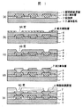
図1は多層配線構造の半導体装置の製造工程図である。図において、回路素子を有するSi基板等の半導体基板は、回路素子の所定部分を除いてシリコン酸化膜等の保護膜2で被覆され、露出した回路素子上に第1導体層が形成されている。前記半導体基板上にスピンコート法等で層間絶縁膜としてのポリイミド樹脂等の膜4が形成される(工程(a))。
【0046】
次に塩化ゴム系またはフェノールノボラック系の感光性樹脂層5が前記層間絶縁膜4上にスピンコート法で形成され、公知の写真食刻技術によって所定部分の層間絶縁膜4が露出するように窓6Aが設けられている(工程(b))。
前記窓6Aの層間絶縁膜4は、酸素、四フッ化炭素等のガスを用いるドライエッチング手段によって選択的にエッチングされ、窓6Bがあけられている。ついで窓6Bから露出した第1導体層3を腐食することなく、感光樹脂層5のみを腐食するようなエッチング溶液を用いて感光樹脂層5が完全に除去される(工程 (c))。
【0047】
さらに公知の写真食刻技術を用いて、第2導体層7を形成させ、第1導体層3との電気的接続が完全に行われる(工程(d))。
3層以上の多層配線構造を形成する場合は、上記の工程を繰り返して行い各層を形成することができる。
【0048】
次に表面保護膜8が形成される。この図の例では、この表面保護膜を前記感光性樹脂組成物をスピンコート法にて塗布、乾燥し、所定部分に窓6Cを形成するパターンを描いたマスク上から光を照射した後アルカリ水溶液にて現像してパターンを形成し、加熱してポリベンゾオキサゾール膜とする。このポリベンゾオキサゾール膜は、導体層を外部からの応力、α線などから保護するものであり、得られる半導体装置は信頼性に優れる。
なお、上記例において、層間絶縁膜を本発明の感光性樹脂組成物を用いて形成することも可能である。
【0049】
【実施例】
以下、本発明を実施例により説明する。
実施例1
攪拌機及び温度計を備えた0.5リットルのフラスコ中に、1,3−アダマンタンジカルボン酸18.8g(0.084モル)及びN−メチルピロリドン(NMP)125gを仕込み、フラスコを0℃に冷却し、塩化チオニル20.0g (0.168モル)を反応温度を10℃以下に保持しながら滴下し、滴下後10℃付近で30分間撹拌して、1,3−ジカルボキシアダマンタンジクロリドの溶液(α)を得た。
【0050】
次いで、攪拌機及び温度計を備えた0.5リットルのフラスコ中に、N−メチルピロリドン100gを仕込み、2,2−ビス(3−アミノ−4−ヒドロキシフェニル)−1,1,1,3,3,3−ヘキサフルオロプロパン23.4g(0.10モル)を添加し、攪拌溶解した後、ピリジン26.6gを添加した。この溶液を冷却し、温度を0〜10℃に保ちながら、1,3−ジカルボキシアダマンタンジクロリドの溶液(α)を30分間かけて滴下した後、10℃付近で30分間撹拌した。
反応液を4リットルの水に投入し、析出物を回収、洗浄した後、40℃で二日間減圧乾燥してポリヒドロキシアミドを得た。
なお、この重量平均分子量は、35,000であった。
【0051】
このポリヒドロキシアミドをγ−ブチロラクトンの溶液にし、厚さ0.2mmのガラス板上にスピンコートで塗布して、膜厚10μmのプリベーク膜を形成した。このプリベーク膜のi線透過率を分光光度計を用いて測定した。その結果98%であった。また、硬化膜の比誘電率は2.65(1KHz)であった。
【0052】
ポリヒドロキシアミド15.00g及びトリス(4−ヒドロキシフェニル)メタンとナフトキノン−1,2−ジアジド−4−スルホニルクロリドを、1/2.9のモル比で反応させたオルトキノンジアジド化合物2.25g、3,3’−メチレンビス(2−ヒドロキシ−5−メチルベンゼンメタノール)1.5g、ジフェニルヨードニウムニトラート0.15g及び尿素プロピルトリエトキシシランの50%メタノール溶液0.30gを、N−メチルピロリドン23.00gに攪拌溶解した。この溶液を3μm孔のテフロンフィルタを用いて加圧濾過して感光性重合体組成物を得た。
【0053】
得られた感光性樹脂組成物をスピンナーによりシリコンウェハ上に回転塗布し、ホットプレート上110℃で3分間加熱乾燥を行い、17μmの塗膜を得た。この塗膜に露光機としてi線ステッパ(株式会社日立製作所製)を用い、レティクルを介し、100〜500mJ/cm2の露光をした。次いで、テトラメチルアンモニウムヒドロキシドの2.38重量%水溶液を現像液とし60秒間パドル現像を行い、純水で洗浄してレリーフパターンを得た。パターン観察により、適正露光量は250mJ/cm2と判断され、この露光量で良好な形状のパターンが形成された。解像度は4μmであった。未露光部の残膜率は83%であった。得られたレリーフパターンを窒素雰囲気下、350℃で1時間加熱処理したところ、良好な形状のポリベンズオキサゾール膜のパターンが得られた。
【0054】
実施例2〜3及び比較例1
表1に示すジカルボン酸とジアミンを用い、実施例1と同様に合成、評価を行った。結果を表2に示す。
【0055】
【表1】
【0056】
【表2】
【0057】
【発明の効果】
本発明のポリベンゾオキサゾール前駆体は、良好なi線透過性とポリベンゾオキサゾール化後の低い比誘電率及び高耐熱性を有する。従って、これを用いたアルカリ現像型感光性樹脂組成物に好適である。
また、本発明のポリベンゾオキサゾールは、低い比誘電率と高耐熱性を両立するものである。従って、ポリベンゾオキサゾール膜形成後の比誘電率が究めて小さく、高耐熱性を有する膜を形成できるため、これを用いた電子部品は、信頼性の高いものである。
【図面の簡単な説明】
【図1】多層配線構造の半導体装置の製造工程図である。
【符号の説明】
1…半導体基板
2…保護膜
3…第1導体層
4…層間絶縁膜層
5…感光樹脂層
6A、6B、6C…窓
7…第2導体層
8…表面保護膜層[0001]
TECHNICAL FIELD OF THE INVENTION
The present invention relates to polybenzoxazole giving a low dielectric constant, a precursor thereof, a photosensitive resin composition using the same, and an electronic component using the same.
[0002]
[Prior art]
Conventionally, as a surface protective film or an interlayer insulating film of a semiconductor element, polyimide is widely used because of its advantages such as excellent heat resistance, excellent mechanical properties and electrical properties, easy film formation, and flattened surface. ing.
When polyimide is used as a surface protective film or an interlayer insulating film, the process of forming through holes and the like is mainly performed by an etching process using a positive photoresist. However, there is a problem that the process involves coating and peeling of a photoresist, which is complicated. Therefore, heat-resistant materials having both photosensitivity have been studied for the purpose of streamlining work steps.
[0003]
Regarding the photosensitive polyimide composition, 1. A polyimide precursor composition having a photosensitive group introduced through an ester bond (Japanese Patent Publication No. 52-30207, etc.); A composition (for example, Japanese Patent Publication No. 3-36861) in which a compound containing a carbon-carbon double bond and an amino group and an aromatic bisazide which can be dimerized or polymerized by irradiation with actinic radiation to a polyamic acid is added. Used.
[0004]
When using the photosensitive polyimide composition, it is usually applied in a solution state on a substrate, dried, irradiated with an actinic ray through a mask, and the exposed portion is removed with a developer to form a pattern.
The compositions 1 and 2 are of a negative type using an organic solvent for a developer. An organic solvent developer has a large burden on the environment when processing waste liquid, and in recent years, in consideration of the environment, a photosensitive heat-resistant material that can be developed with an aqueous developer that is easy to process the waste developer has been required. . In addition, in order to switch from an etching process using a positive photoresist to a negative photosensitive polyimide, it is necessary to change a mask of an exposure apparatus and development equipment. The compositions 1 and 2 have the problems as described above.
[0005]
On the other hand, as the positive photosensitive polyimide, 3. a polyimide precursor having an o-nitrobenzyl group introduced through an ester bond (JP-A-60-37550); A composition containing a polyamic acid ester containing a phenolic hydroxyl group and an o-diazoquinone compound (JP-A-4-204945) is known. 4. A photosensitive material using polybenzoxazole having heat resistance, mechanical properties, and electrical properties equivalent to polyimide as a positive heat-resistant material. Compositions containing a polybenzoxazole precursor and an o-diazoquinone compound (JP-A-64-6947, JP-A-9-302221, etc.) are also known.
[0006]
However, the above-mentioned 3 has a problem that the sensitivity is low because the photosensitive wavelength is mainly 300 nm or less, and it is difficult to use it particularly with an i-line stepper (single-wavelength light of 365 nm) which is recently used. The compositions 4 and 5 have higher sensitivity than the precursor 3 but have a problem that they are not sufficient. Thus, at present, a positive photosensitive heat-resistant material having sufficient sensitivity has not been obtained.
[0007]
[Problems to be solved by the invention]
The present invention provides a polybenzoxazole precursor having good i-line transmittance, low dielectric constant after polybenzoxazole conversion, and high heat resistance in the polybenzoxazole precursor, and a photosensitive resin composition using the same. Is what you do.
The present invention also provides a polybenzoxazole having a low dielectric constant and high heat resistance.
Further, the present invention provides an electronic component having a very low relative dielectric constant after forming a polybenzoxazole film and having excellent reliability using a film having high heat resistance.
[0008]
[Means for Solving the Problems]
The present invention relates to general formula (1)
Embedded image
(Wherein X is a divalent organic group, Y is a tetravalent organic group, and both or one of X and Y has an adamantane structure in the main chain). It relates to an oxazole precursor.
[0009]
Further, in the present invention, the precursor has an i-line transmittance of 10% or more per 10 μm in film thickness, and a polybenzoxazole film formed by dehydrating and ring-closing this polybenzoxazole precursor has a relative dielectric constant of 2%. A polybenzoxazole precursor which is less than 0.8.
In the present invention, the general formula (1) is preferably
Embedded image
Wherein Y is a tetravalent organic group.
[0010]
The present invention also relates to a photosensitive resin composition containing the above-mentioned polybenzoxazole precursor and a photosensitive agent.
Further, the present invention provides a compound represented by the general formula (3):
Embedded image
Wherein X is a divalent organic group, Y is a tetravalent organic group, and both or one of X and Y has an alicyclic structure in the main chain. A benzoxazole precursor having an i-line transmittance of 10% or more per 10 μm of film thickness, and a polybenzoxazole film formed by dehydration-closing this polybenzoxazole precursor to have a relative dielectric constant of 2.8. The present invention relates to a photosensitive resin composition containing a polybenzoxazole precursor and a photosensitive agent.
[0011]
The present invention also relates to a photosensitive resin composition wherein the photosensitive agent is a compound that generates an acid by light.
The present invention also relates to a polybenzoxazole formed by dehydrating and ring-closing the polybenzoxazole precursor.
Furthermore, the present invention relates to an electronic component having the above-mentioned polybenzoxazole film as a surface protective film or an interlayer insulating film.
[0012]
BEST MODE FOR CARRYING OUT THE INVENTION
The polybenzoxazole precursor of the present invention has a repeating unit represented by the general formula (1). In the general formula (1), it is necessary that either X or Y has an adamantane structure. However, the precursor exhibits high light transmittance, and the polybenzoxazole film has a low relative dielectric constant and a high heat resistance. In order to achieve both, it is particularly preferable that X has an adamantane structure. In this case, Y may be any structure that does not decrease the light transmittance of the precursor and the relative dielectric constant and heat resistance of the polybenzoxazole film. For example, a discontinuous aromatic ring structure (where aromatic rings are linked via a divalent group) A structure in which the aromatic ring is twisted or a structure containing a fluorine atom is preferable even when the aromatic ring is continuous (a structure in which the aromatic rings are directly covalently bonded) or when the aromatic rings are continuous (a structure in which the aromatic rings are directly covalently bonded).
[0013]
The polybenzoxazole precursor of the present invention has an i-line transmittance of preferably 10%, more preferably 30% or more, even more preferably 50 to 100% per 10 μm of prebaked film thickness. . If the transmittance is low, the pattern properties (sensitivity and resolution) decrease.
In the measurement of i-line transmittance, the prebaked film thickness can be adjusted by the concentration of the polybenzoxazole precursor solution, the spin speed at the time of coating, and the like. Specifically, a polybenzoxazole precursor solution is applied on a glass plate having a thickness of 0.2 mm by spin coating, and then the solvent is volatilized on a hot plate to prepare a prebaked film. The prebaking conditions are preferably 80 ° C. × 100 seconds and 95 ° C. × 100 seconds. In the examples described later, this method was used. The measurement of the prebaked film thickness can be performed by a stylus type surface roughness meter. The measurement of the i-line transmittance can be performed by a spectrophotometer.
[0014]
Further, the polybenzoxazole precursor of the present invention preferably has a relative dielectric constant of less than 2.8. When the ratio is 2.8 or more, there is a disadvantage that a signal delay in the wiring portion becomes obvious. The relative permittivity is measured as follows. That is, after spin-coating a polybenzoxazole precursor solution on a low-resistance silicon wafer by a spinner, and heating and curing at 350 ° C. for 1 hour, a 5 mmφ aluminum electrode is formed on a cured film (thickness: 10 μm) by vacuum evaporation. To form Next, the charge capacity between the aluminum electrode and the low-resistance silicon wafer is measured using an impedance analyzer, and the relative permittivity can be calculated from the obtained value.
[0015]
The polybenzoxazole precursor having the above-mentioned i-line transmittance can be adjusted, for example, by introducing an alicyclic structure. Generally, the alicyclic structure has a disadvantage that the thermal decomposition temperature is low. However, since the adamantane structure in the polybenzoxazole precursor of the present invention has a structure bridging the alicyclic structure, i-line permeability and heat resistance are reduced. Can be compatible.
[0016]
In the present invention, the polybenzoxazole precursor having a repeating unit represented by the general formula (1) can be generally synthesized from a dicarboxylic acid derivative and a hydroxy group-containing diamine. Specifically, it can be synthesized by converting a dicarboxylic acid derivative into a dihalide derivative and then reacting with the diamine. As the dihalide derivative, a dichloride derivative is preferable.
[0017]
The dichloride derivative can be synthesized by reacting a dicarboxylic acid derivative with a halogenating agent. As the halogenating agent, thionyl chloride, phosphoryl chloride, phosphorus oxychloride, phosphorus pentachloride, and the like, which are commonly used in acid chlorination of carboxylic acids, can be used.
[0018]
The dichloride derivative can be synthesized by reacting the dicarboxylic acid derivative with the halogenating agent in a solvent or by performing the reaction in an excess of the halogenating agent and then distilling off the excess. As the reaction solvent, N-methyl-2-pyrrolidone, N-methyl-2-pyridone, N, N-dimethylacetamide, N, N-dimethylformamide, toluene, benzene and the like can be used.
[0019]
When used in a solvent, the amount of these halogenating agents used is preferably 1.5 to 3.0 mol, more preferably 1.7 to 2.5 mol, per 1 mol of the dicarboxylic acid derivative. When reacting in a halogenating agent, 4.0 to 50 mol is preferable, and 5.0 to 20 mol is more preferable. The reaction temperature is preferably from -10 to 70C, more preferably from 0 to 20C.
[0020]
The reaction between the dichloride derivative and the diamine is preferably performed in an organic solvent in the presence of a dehydrohalogenating agent. As the dehydrohalogenating agent, an organic base such as pyridine and triethylamine is usually used. As the organic solvent, N-methyl-2-pyrrolidone, N-methyl-2-pyridone, N, N-dimethylacetamide, N, N-dimethylformamide and the like can be used. The reaction temperature is preferably from -10 to 30C, more preferably from 0 to 20C.
[0021]
Here, in the general formula (1), a tetravalent organic group represented by Y generally means that two hydroxy groups which react with a dicarboxylic acid to form a polyamide structure are each in the ortho position of the amino group. It is a residue of a diamine having a located structure. Specifically, an aromatic group having a tetravalent adamantane structure or another alicyclic structure is preferable. The number of carbon atoms is preferably from 6 to 40, and more preferably a tetravalent aromatic group having from 6 to 40 carbon atoms. As the tetravalent aromatic group, a group in which all four binding sites are present on an aromatic ring is preferable.
[0022]
Such diamines having an adamantane structure in the main chain include:
Embedded image
(In each formula, Z represents any of O, CO, and COO.).
[0023]
Further, as other diamines having an alicyclic structure,
Embedded image
(In each formula, Z represents any one of O, CO, and COO.).
[0024]
In addition, 3,3′-diamino-4,4′-dihydroxybiphenyl, 4,4′-diamino-3,3′-dihydroxybiphenyl, bis (3-amino-4-hydroxyphenyl) propane, bis (4-amino -3-hydroxyphenyl) propane, bis (3-amino-4-hydroxyphenyl) sulfone, bis (4-amino-3-hydroxyphenyl) sulfone, 2,2-bis (3-amino-4-hydroxyphenyl)- Fats such as 1,1,1,3,3,3-hexafluoropropane and 2,2-bis (4-amino-3-hydroxyphenyl) -1,1,1,3,3,3-hexafluoropropane Aromatic diamines having no ring structure may be mentioned. Furthermore, it is also possible to use an alicyclic diamine or an aliphatic diamine together to such an extent that the effects of the present invention are not impaired.
These compounds can be used alone or in combination of two or more.
[0025]
In the general formula (1), the divalent organic group represented by X is a residue of a dicarboxylic acid that reacts with a diamine to form a polyamide structure, and is a divalent alicyclic having an adamantane structure. The structure is preferred, and the number of carbon atoms is preferably 10 to 40, more preferably a divalent alicyclic structure having 10 to 40 carbon atoms. A more preferred divalent alicyclic structure is one in which both of the two binding sites are present on the adamantane structure.
[0026]
As a dicarboxylic acid having such an adamantane structure,
Embedded image
(In each formula, Z represents any one of O, CO, and COO.).
These compounds can be used alone or in combination of two or more.
[0027]
In the general formula (1), when Y has an adamantane structure, or when used in combination with the dicarboxylic acid having the adamantane structure, preferably, the i-line transmittance of the polybenzoxazole precursor film is not significantly reduced. Aromatic dicarboxylic acids or other aliphatic dicarboxylic acids may be copolymerized.
Examples of such aromatic dicarboxylic acids include isophthalic acid, terephthalic acid, 2,2-bis (4-carboxyphenyl) -1,1,1,3,3,3-hexafluoropropane and 4,4′-dicarboxylic acid. Carboxybiphenyl, 4,4'-dicarboxydiphenyl ether, 4,4'-dicarboxytetraphenylsilane, bis (4-carboxyphenyl) sulfone, 2,2-bis (p-carboxyphenyl) propane, 5-tert-butyl Aromatic dicarboxylic acids such as isophthalic acid, 5-bromoisophthalic acid, 5-fluoroisophthalic acid, 5-chloroisophthalic acid, 2,6-naphthalenedicarboxylic acid, 1,2-cyclobutanedicarboxylic acid, 1,4-cyclohexanedicarboxylic acid Aliphatics such as acid, 1,3-cyclopentanedicarboxylic acid, oxalic acid, malonic acid, and succinic acid Such as dicarboxylic acid, and the like.
[0028]
Further, as a dicarboxylic acid having another alicyclic structure,
Embedded image
(R in each formula is CH 3 , C 2 H 5 Alkyl groups such as 6 H 5 And the like).
These compounds can be used alone or in combination of two or more.
[0029]
The molecular weight of the polybenzoxazole precursor of the present invention is not particularly limited, but is generally preferably 5,000 to 500,000, more preferably 10,000 to 50,000, in terms of weight average molecular weight. The weight average molecular weight can be measured by a gel permeation chromatography method and converted using a standard polystyrene calibration curve.
[0030]
In the photosensitive resin composition of the present invention, it is preferable in terms of characteristics to use the polybenzoxazole precursor having the adamantane structure. However, other than the above, a polybenzoxazole having a repeating unit represented by the general formula (3) is preferably used. A benzoxazole precursor (that is, both or one of the repeating units X and Y has an alicyclic structure in the main chain), and has an i-line transmittance of 10% or more per 10 μm of film thickness; A polybenzoxazole precursor in which the relative permittivity of the polybenzoxazole film formed by dehydrating and ring-closing the benzoxazole precursor is less than 2.8 can also be used.
[0031]
The photosensitive resin composition of the present invention contains a photosensitive agent together with the polybenzoxazole precursor. The photosensitive agent has a function of changing the solubility of a film formed from the composition in a developer in response to light. The photosensitive agent is not particularly limited, but a compound capable of generating an acid by light is generally used in a positive photosensitive resin composition. This has the function of generating an acid and increasing the solubility of the irradiated portion in an aqueous alkaline solution. Examples of the type include an o-quinonediazide compound, an aryldiazonium salt, a diaryliodonium salt, and a triarylsulfonium salt. There is no particular limitation, but an o-quinonediazide compound is preferred because of its high sensitivity.
[0032]
The o-quinonediazide compound is obtained, for example, by subjecting an o-quinonediazide sulfonyl chloride to a condensation reaction with a hydroxy compound, an amino compound and the like in the presence of a dehydrochlorinating agent.
Examples of the o-quinonediazide sulfonyl chloride include benzoquinone-1,2-diazide-4-sulfonyl chloride, naphthoquinone-1,2-diazide-5-sulfonyl chloride, naphthoquinone-1,2-diazide-4-sulfonyl chloride. Etc. can be used.
[0033]
Examples of the hydroxy compound include hydroquinone, resorcinol, pyrogallol, bisphenol A, bis (4-hydroxyphenyl) methane, 2,2-bis (4-hydroxyphenyl) hexafluoropropane, and 2,3,4-trihydroxybenzophenone 2,3,4,4′-tetrahydroxybenzophenone, 2,2 ′, 4,4′-tetrahydroxybenzophenone, 2,3,4,2 ′, 3′-pentahydroxybenzophenone, 2,3,4 3 ', 4', 5'-hexahydroxybenzophenone, bis (2,3,4-trihydroxyphenyl) methane, bis (2,3,4-trihydroxyphenyl) propane, 4b, 5,9b, 10-tetrahydro -1,3,6,8-Tetrahydroxy-5,10-dimethylindeno [2,1-a] i Den, tris (4-hydroxyphenyl) methane, and tris (4-hydroxyphenyl) ethane can be used.
[0034]
Examples of the amino compound include p-phenylenediamine, m-phenylenediamine, 4,4′-diaminodiphenyl ether, 4,4′-diaminodiphenylmethane, 4,4′-diaminodiphenylsulfone, and 4,4′-diaminodiphenylsulfide , O-aminophenol, m-aminophenol, p-aminophenol, 3,3'-diamino-4,4'-dihydroxybiphenyl, 4,4'-diamino-3,3'-dihydroxybiphenyl, bis (3- Amino-4-hydroxyphenyl) propane, bis (4-amino-3-hydroxyphenyl) propane, bis (3-amino-4-hydroxyphenyl) sulfone, bis (4-amino-3-hydroxyphenyl) sulfone, bis ( 3-amino-4-hydroxyphenyl) hexafluoropropane Bis (4-amino-3-hydroxyphenyl) hexafluoropropane can be used.
[0035]
The o-quinonediazidosulfonyl chloride and the hydroxy compound and / or the amino compound may be blended such that the total of the hydroxy group and the amino group is 0.5 to 1 mol per 1 mol of the o-quinonediazidosulfonyl chloride. preferable. The preferred ratio between the dehydrochlorinating agent and o-quinonediazide sulfonyl chloride is in the range of 0.95 / 1 to 1 / 0.95. The preferred reaction temperature is 0 to 40 ° C, and the preferred reaction time is 1 to 10 hours.
[0036]
As a reaction solvent, a solvent such as dioxane, acetone, methyl ethyl ketone, tetrahydrofuran, diethyl ether, N-methylpyrrolidone, or the like is used.
Examples of the dehydrochlorinating agent include sodium carbonate, sodium hydroxide, sodium hydrogen carbonate, potassium carbonate, potassium hydroxide, trimethylamine, triethylamine, pyridine and the like.
[0037]
The amount of the photosensitizer is not particularly limited, but is preferably 1 to 50 parts by weight based on 100 parts by weight of the polybenzoxazole precursor from the viewpoint of sensitivity and residual film ratio.
The photosensitive resin composition of the present invention can be obtained by dissolving the polybenzoxazole precursor and the photosensitive agent component as essential components in a solvent.
[0038]
Examples of the solvent include aprotic polar solvents such as N-methyl-2-pyrrolidone, N, N-dimethylformamide, N, N-dimethylacetamide, dimethylsulfoxide, hexamethylphosphorylamide, tetramethylene sulfone, and γ-butyrolactone. And these are used alone or in combination of two or more.
[0039]
In addition, solvents such as diethyl ketone, diisobutyl ketone, methyl amyl ketone, ethyl lactate, and propylene glycol monomethyl ether acetate can be used in combination for improving coating properties.
The amount of the solvent is not particularly limited, but is generally adjusted so that the amount of the solvent in the composition is 20 to 90% by weight.
[0040]
The photosensitive resin composition of the present invention can further contain an organic silane compound, an aluminum chelate compound, or the like as an adhesion assistant, if necessary.
As the organic silane compound, for example, γ-aminopropyltrimethoxysilane, γ-aminopropyltriethoxysilane, vinyltriethoxysilane, γ-glycidoxypropyltriethoxysilane, γ-methacryloxypropyltrimethoxysilane, ureapropyl And triethoxysilane.
Examples of the aluminum chelate compound include aluminum tris (acetylacetonate) and aluminum acetylacetate diisopropylate.
[0041]
The photosensitive resin composition of the present invention can be formed into a relief pattern of polybenzoxazole through a step of coating and drying on a supporting substrate, a step of exposing, a step of developing, and a step of heat treatment.
In the step of coating and drying on a supporting substrate, a glass substrate, a semiconductor, a metal oxide insulator (eg, TiO 2 , SiO 2 Etc.), the photosensitive resin composition is spin-coated on a support substrate such as silicon nitride using a spinner or the like, and then dried using a hot plate, an oven, or the like.
[0042]
Next, in the exposure step, the photosensitive resin composition coated on the supporting substrate is irradiated with actinic light such as ultraviolet light, visible light, or radiation through a mask.
In the developing step, a relief pattern is obtained by removing the exposed portion with a developing solution. Preferred examples of the developer include an aqueous alkali solution such as sodium hydroxide, potassium hydroxide, sodium silicate, ammonia, ethylamine, diethylamine, triethylamine, triethanolamine, and tetramethylammonium hydroxide. The aqueous solution preferably has a base concentration of 0.1 to 10% by weight. Further, an alcohol or a surfactant may be added to the above developer to be used. Each of these may be added in an amount of preferably 0.01 to 10 parts by weight, more preferably 0.1 to 5 parts by weight, based on 100 parts by weight of the developer.
[0043]
Next, in the heat treatment step, a heat-resistant polybenzoxazole pattern having an oxazole ring or another functional group is obtained by subjecting the obtained relief pattern to a heat treatment preferably at 150 to 450 ° C.
[0044]
The photosensitive resin composition of the present invention can be used for electronic components such as semiconductor devices and multilayer wiring boards, and specifically, surface protective films and interlayer insulating films of semiconductor devices, and interlayer insulating films of multilayer wiring boards. Etc. can be used.
The semiconductor device of the present invention is not particularly limited except that it has a surface protective film and an interlayer insulating film formed using the composition, and can have various structures.
[0045]
An example of the semiconductor device manufacturing process of the present invention will be described below.
FIG. 1 is a manufacturing process diagram of a semiconductor device having a multilayer wiring structure. In the figure, a semiconductor substrate such as a Si substrate having a circuit element is covered with a protective film 2 such as a silicon oxide film except for a predetermined portion of the circuit element, and a first conductor layer is formed on the exposed circuit element. . A film 4 of a polyimide resin or the like as an interlayer insulating film is formed on the semiconductor substrate by a spin coating method or the like (step (a)).
[0046]
Next, a photosensitive resin layer 5 of a chlorinated rubber type or a phenol novolak type is formed on the interlayer insulating film 4 by spin coating, and a window is formed by a known photolithography technique so that a predetermined portion of the interlayer insulating film 4 is exposed. 6A is provided (step (b)).
The interlayer insulating film 4 in the window 6A is selectively etched by a dry etching means using a gas such as oxygen or carbon tetrafluoride, and a window 6B is opened. Next, the photosensitive resin layer 5 is completely removed using an etching solution that does not corrode the first conductor layer 3 exposed from the window 6B, but corrodes only the photosensitive resin layer 5 (step (c)).
[0047]
Further, the second conductor layer 7 is formed by using a known photolithography technique, and the electrical connection with the first conductor layer 3 is completely performed (step (d)).
When a multilayer wiring structure having three or more layers is formed, the above steps can be repeated to form each layer.
[0048]
Next, a surface protection film 8 is formed. In the example of this figure, the surface protective film is coated with the photosensitive resin composition by a spin coating method, dried, irradiated with light from a mask on which a pattern for forming a window 6C is formed on a predetermined portion, and then exposed to an alkaline aqueous solution. To form a pattern and heat to form a polybenzoxazole film. This polybenzoxazole film protects the conductor layer from external stress, α-rays, and the like, and the obtained semiconductor device has excellent reliability.
In the above example, the interlayer insulating film can be formed using the photosensitive resin composition of the present invention.
[0049]
【Example】
Hereinafter, the present invention will be described with reference to examples.
Example 1
In a 0.5 liter flask equipped with a stirrer and a thermometer, 18.8 g (0.084 mol) of 1,3-adamantanedicarboxylic acid and 125 g of N-methylpyrrolidone (NMP) were charged, and the flask was cooled to 0 ° C. Then, 20.0 g (0.168 mol) of thionyl chloride was added dropwise while maintaining the reaction temperature at 10 ° C. or lower. After the dropwise addition, the mixture was stirred at about 10 ° C. for 30 minutes to give a solution of 1,3-dicarboxyadamantane dichloride ( α) was obtained.
[0050]
Next, 100 g of N-methylpyrrolidone was charged into a 0.5-liter flask equipped with a stirrer and a thermometer, and 2,2-bis (3-amino-4-hydroxyphenyl) -1,1,1,3,3 was added. 23.4 g (0.10 mol) of 3,3-hexafluoropropane was added, and the mixture was stirred and dissolved. Then, 26.6 g of pyridine was added. This solution was cooled, and while maintaining the temperature at 0 to 10 ° C, a solution (α) of 1,3-dicarboxyadamantane dichloride was added dropwise over 30 minutes, followed by stirring at around 10 ° C for 30 minutes.
The reaction solution was poured into 4 liters of water, and the precipitate was collected and washed, and then dried under reduced pressure at 40 ° C. for 2 days to obtain polyhydroxyamide.
The weight average molecular weight was 35,000.
[0051]
This polyhydroxyamide was converted to a solution of γ-butyrolactone, and applied by spin coating on a glass plate having a thickness of 0.2 mm to form a prebaked film having a thickness of 10 μm. The i-ray transmittance of the prebaked film was measured using a spectrophotometer. As a result, it was 98%. The relative permittivity of the cured film was 2.65 (1 KHz).
[0052]
Orthoquinone diazide compound (15.00 g), tris (4-hydroxyphenyl) methane and naphthoquinone-1,2-diazide-4-sulfonyl chloride (2.25 g, 3/25) were reacted at a molar ratio of 1 / 2.9. 1.5 g of 3,3'-methylenebis (2-hydroxy-5-methylbenzenemethanol), 0.15 g of diphenyliodonium nitrate and 0.30 g of a 50% methanol solution of ureapropyltriethoxysilane were added to 23.00 g of N-methylpyrrolidone. Was dissolved by stirring. This solution was filtered under pressure using a Teflon filter having a pore size of 3 μm to obtain a photosensitive polymer composition.
[0053]
The obtained photosensitive resin composition was spin-coated on a silicon wafer by a spinner and dried by heating at 110 ° C. for 3 minutes on a hot plate to obtain a 17 μm coating film. Using an i-line stepper (manufactured by Hitachi, Ltd.) as an exposure machine on this coating film, through a reticle, 100 to 500 mJ / cm. 2 Was exposed. Next, paddle development was performed for 60 seconds using a 2.38% by weight aqueous solution of tetramethylammonium hydroxide as a developing solution, followed by washing with pure water to obtain a relief pattern. By pattern observation, the proper exposure is 250 mJ / cm 2 Thus, a pattern having a good shape was formed at this exposure amount. The resolution was 4 μm. The residual film ratio of the unexposed portion was 83%. When the obtained relief pattern was heated at 350 ° C. for 1 hour in a nitrogen atmosphere, a pattern of a polybenzoxazole film having a good shape was obtained.
[0054]
Examples 2-3 and Comparative Example 1
Synthesis and evaluation were performed in the same manner as in Example 1 using the dicarboxylic acids and diamines shown in Table 1. Table 2 shows the results.
[0055]
[Table 1]
[0056]
[Table 2]
[0057]
【The invention's effect】
The polybenzoxazole precursor of the present invention has good i-line transmittance, low dielectric constant after polybenzoxazole conversion, and high heat resistance. Therefore, it is suitable for an alkali development type photosensitive resin composition using the same.
Further, the polybenzoxazole of the present invention has both a low relative dielectric constant and high heat resistance. Accordingly, the relative permittivity after the formation of the polybenzoxazole film is extremely small, and a film having high heat resistance can be formed. Therefore, an electronic component using the film has high reliability.
[Brief description of the drawings]
FIG. 1 is a manufacturing process diagram of a semiconductor device having a multilayer wiring structure.
[Explanation of symbols]
1 .... Semiconductor substrate
2 ... Protective film
3. First conductor layer
4: Interlayer insulating film layer
5. Photosensitive resin layer
6A, 6B, 6C… Window
7 Second conductor layer
8: Surface protective film layer