JP2004104155A - 半導体装置 - Google Patents
半導体装置 Download PDFInfo
- Publication number
- JP2004104155A JP2004104155A JP2003433161A JP2003433161A JP2004104155A JP 2004104155 A JP2004104155 A JP 2004104155A JP 2003433161 A JP2003433161 A JP 2003433161A JP 2003433161 A JP2003433161 A JP 2003433161A JP 2004104155 A JP2004104155 A JP 2004104155A
- Authority
- JP
- Japan
- Prior art keywords
- die pad
- semiconductor device
- semiconductor element
- sealing
- sealing resin
- Prior art date
- Legal status (The legal status is an assumption and is not a legal conclusion. Google has not performed a legal analysis and makes no representation as to the accuracy of the status listed.)
- Pending
Links
Images




Classifications
-
- H—ELECTRICITY
- H10—SEMICONDUCTOR DEVICES; ELECTRIC SOLID-STATE DEVICES NOT OTHERWISE PROVIDED FOR
- H10W—GENERIC PACKAGES, INTERCONNECTIONS, CONNECTORS OR OTHER CONSTRUCTIONAL DETAILS OF DEVICES COVERED BY CLASS H10
- H10W72/00—Interconnections or connectors in packages
- H10W72/01—Manufacture or treatment
- H10W72/011—Apparatus therefor
- H10W72/0113—Apparatus for manufacturing die-attach connectors
-
- H—ELECTRICITY
- H10—SEMICONDUCTOR DEVICES; ELECTRIC SOLID-STATE DEVICES NOT OTHERWISE PROVIDED FOR
- H10W—GENERIC PACKAGES, INTERCONNECTIONS, CONNECTORS OR OTHER CONSTRUCTIONAL DETAILS OF DEVICES COVERED BY CLASS H10
- H10W72/00—Interconnections or connectors in packages
- H10W72/071—Connecting or disconnecting
- H10W72/073—Connecting or disconnecting of die-attach connectors
-
- H—ELECTRICITY
- H10—SEMICONDUCTOR DEVICES; ELECTRIC SOLID-STATE DEVICES NOT OTHERWISE PROVIDED FOR
- H10W—GENERIC PACKAGES, INTERCONNECTIONS, CONNECTORS OR OTHER CONSTRUCTIONAL DETAILS OF DEVICES COVERED BY CLASS H10
- H10W72/00—Interconnections or connectors in packages
- H10W72/071—Connecting or disconnecting
- H10W72/075—Connecting or disconnecting of bond wires
-
- H—ELECTRICITY
- H10—SEMICONDUCTOR DEVICES; ELECTRIC SOLID-STATE DEVICES NOT OTHERWISE PROVIDED FOR
- H10W—GENERIC PACKAGES, INTERCONNECTIONS, CONNECTORS OR OTHER CONSTRUCTIONAL DETAILS OF DEVICES COVERED BY CLASS H10
- H10W72/00—Interconnections or connectors in packages
- H10W72/50—Bond wires
- H10W72/551—Materials of bond wires
- H10W72/552—Materials of bond wires comprising metals or metalloids, e.g. silver
- H10W72/5522—Materials of bond wires comprising metals or metalloids, e.g. silver comprising gold [Au]
-
- H—ELECTRICITY
- H10—SEMICONDUCTOR DEVICES; ELECTRIC SOLID-STATE DEVICES NOT OTHERWISE PROVIDED FOR
- H10W—GENERIC PACKAGES, INTERCONNECTIONS, CONNECTORS OR OTHER CONSTRUCTIONAL DETAILS OF DEVICES COVERED BY CLASS H10
- H10W72/00—Interconnections or connectors in packages
- H10W72/851—Dispositions of multiple connectors or interconnections
- H10W72/874—On different surfaces
- H10W72/884—Die-attach connectors and bond wires
-
- H—ELECTRICITY
- H10—SEMICONDUCTOR DEVICES; ELECTRIC SOLID-STATE DEVICES NOT OTHERWISE PROVIDED FOR
- H10W—GENERIC PACKAGES, INTERCONNECTIONS, CONNECTORS OR OTHER CONSTRUCTIONAL DETAILS OF DEVICES COVERED BY CLASS H10
- H10W74/00—Encapsulations, e.g. protective coatings
- H10W74/10—Encapsulations, e.g. protective coatings characterised by their shape or disposition
- H10W74/111—Encapsulations, e.g. protective coatings characterised by their shape or disposition the semiconductor body being completely enclosed
- H10W74/127—Encapsulations, e.g. protective coatings characterised by their shape or disposition the semiconductor body being completely enclosed characterised by arrangements for sealing or adhesion
-
- H—ELECTRICITY
- H10—SEMICONDUCTOR DEVICES; ELECTRIC SOLID-STATE DEVICES NOT OTHERWISE PROVIDED FOR
- H10W—GENERIC PACKAGES, INTERCONNECTIONS, CONNECTORS OR OTHER CONSTRUCTIONAL DETAILS OF DEVICES COVERED BY CLASS H10
- H10W90/00—Package configurations
- H10W90/701—Package configurations characterised by the relative positions of pads or connectors relative to package parts
- H10W90/731—Package configurations characterised by the relative positions of pads or connectors relative to package parts of die-attach connectors
- H10W90/736—Package configurations characterised by the relative positions of pads or connectors relative to package parts of die-attach connectors between a chip and a stacked lead frame, conducting package substrate or heat sink
-
- H—ELECTRICITY
- H10—SEMICONDUCTOR DEVICES; ELECTRIC SOLID-STATE DEVICES NOT OTHERWISE PROVIDED FOR
- H10W—GENERIC PACKAGES, INTERCONNECTIONS, CONNECTORS OR OTHER CONSTRUCTIONAL DETAILS OF DEVICES COVERED BY CLASS H10
- H10W90/00—Package configurations
- H10W90/701—Package configurations characterised by the relative positions of pads or connectors relative to package parts
- H10W90/751—Package configurations characterised by the relative positions of pads or connectors relative to package parts of bond wires
- H10W90/756—Package configurations characterised by the relative positions of pads or connectors relative to package parts of bond wires between a chip and a stacked lead frame, conducting package substrate or heat sink
Landscapes
- Lead Frames For Integrated Circuits (AREA)
Abstract
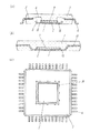
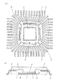
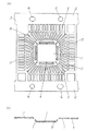
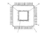
【解決手段】ダイパッド1の側面に複数の突起部9を設け、その突起部9を半導体素子3の搭載面側に折り曲げるようにリードフレームを加工する。そして、搭載面上に半導体素子3を搭載し、ダイパッド1の露出面を露出させて、半導体素子3、突起部9、インナーリード等を封止樹脂体7で封止する。すると、突起部9およびそれらの連結部分が封止樹脂体7に噛み合い密着性が向上。実装時のダイパッド1の変形が少なく、実装後も良好な耐湿性を維持できる。
【選択図】図3
Description
2 接着剤
3 半導体素子
4 金属細線
5 インナーリード
6 アウターリード
7 封止樹脂体
8 突起部
9 突起部
10 支持リード
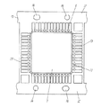
11 ダムバー
12 外枠
13 内枠
14 ガイド孔
15 リードフレーム
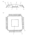
16 溝
17 ステージ
18 ディスペンサ
19 コレット
20 ヒートステージ
21 ボンディングパッド
22 固定治具
23 リードフレーム重合体
24 上型
25 下型
26a キャビティー上
26b キャビティー下
27 ポット
28 プランジャー
29 カル
30 ランナー
31 ゲート
32 逃がし部
33 薄バリ
Claims (4)
- 半導体素子と、
前記半導体素子を搭載するダイパッドと、
前記半導体素子を封止する封止樹脂体と、
前記ダイパッドは、前記半導体素子を搭載する搭載面と、前記封止樹脂体から外へ露出されている前記搭載面と反対側の露出面とを有し、
前記露出面の周縁に沿って溝が設けられた、半導体装置。 - 前記溝は前記半導体チップよりも外側に形成されている、請求項1に記載の半導体装置。
- 前記溝はリング状に形成されている、請求項1または請求項2に記載の半導体装置。
- 前記溝は二重に形成されている、請求項1〜請求項3のいずれかひとつに記載の半導体装置。
Priority Applications (1)
| Application Number | Priority Date | Filing Date | Title |
|---|---|---|---|
| JP2003433161A JP2004104155A (ja) | 2003-12-26 | 2003-12-26 | 半導体装置 |
Applications Claiming Priority (1)
| Application Number | Priority Date | Filing Date | Title |
|---|---|---|---|
| JP2003433161A JP2004104155A (ja) | 2003-12-26 | 2003-12-26 | 半導体装置 |
Related Parent Applications (1)
| Application Number | Title | Priority Date | Filing Date |
|---|---|---|---|
| JP36707598A Division JP3606078B2 (ja) | 1998-12-24 | 1998-12-24 | 半導体装置およびその製造方法 |
Publications (1)
| Publication Number | Publication Date |
|---|---|
| JP2004104155A true JP2004104155A (ja) | 2004-04-02 |
Family
ID=32291296
Family Applications (1)
| Application Number | Title | Priority Date | Filing Date |
|---|---|---|---|
| JP2003433161A Pending JP2004104155A (ja) | 2003-12-26 | 2003-12-26 | 半導体装置 |
Country Status (1)
| Country | Link |
|---|---|
| JP (1) | JP2004104155A (ja) |
Cited By (2)
| Publication number | Priority date | Publication date | Assignee | Title |
|---|---|---|---|---|
| JP2006135100A (ja) * | 2004-11-05 | 2006-05-25 | Matsushita Electric Ind Co Ltd | 半導体装置及びその製造方法 |
| IT202300021597A1 (it) * | 2023-10-17 | 2025-04-17 | St Microelectronics Int Nv | Procedimento per fabbricare dispositivi a semiconduttore e dispositivo a semiconduttore corrispondente |
-
2003
- 2003-12-26 JP JP2003433161A patent/JP2004104155A/ja active Pending
Cited By (3)
| Publication number | Priority date | Publication date | Assignee | Title |
|---|---|---|---|---|
| JP2006135100A (ja) * | 2004-11-05 | 2006-05-25 | Matsushita Electric Ind Co Ltd | 半導体装置及びその製造方法 |
| IT202300021597A1 (it) * | 2023-10-17 | 2025-04-17 | St Microelectronics Int Nv | Procedimento per fabbricare dispositivi a semiconduttore e dispositivo a semiconduttore corrispondente |
| EP4542629A1 (en) | 2023-10-17 | 2025-04-23 | STMicroelectronics International N.V. | Method of manufacturing semiconductor devices and corresponding semiconductor device |
Similar Documents
| Publication | Publication Date | Title |
|---|---|---|
| US6338984B2 (en) | Resin-molded semiconductor device, method for manufacturing the same, and leadframe | |
| EP0977251B1 (en) | Resin sealed semiconductor device and method for manufacturing the same | |
| US6455348B1 (en) | Lead frame, resin-molded semiconductor device, and method for manufacturing the same | |
| US6638790B2 (en) | Leadframe and method for manufacturing resin-molded semiconductor device | |
| JPH11340409A (ja) | リードフレームおよびその製造方法ならびに樹脂封止型半導体装置およびその製造方法 | |
| JP3606078B2 (ja) | 半導体装置およびその製造方法 | |
| JP3535760B2 (ja) | 樹脂封止型半導体装置,その製造方法及びリードフレーム | |
| JP2000236060A (ja) | 半導体装置 | |
| JPH11260990A (ja) | リードフレーム,樹脂封止型半導体装置及びその製造方法 | |
| JP2006191143A (ja) | 半導体装置 | |
| JP2004104155A (ja) | 半導体装置 | |
| JP4308698B2 (ja) | 半導体装置 | |
| JP4066050B2 (ja) | 樹脂封止型半導体装置及びその製造方法 | |
| JP2007134585A (ja) | 半導体装置及びその製造方法 | |
| JP3007632B1 (ja) | 樹脂封止型半導体装置およびその製造方法 | |
| JP2002134654A (ja) | 樹脂封止型半導体装置及びその製造方法 | |
| JP2006216993A (ja) | 樹脂封止型半導体装置 | |
| JP2005158771A (ja) | 半導体装置およびその製造方法 | |
| JP6332053B2 (ja) | 半導体装置及びその製造方法 | |
| JP2004207307A (ja) | 半導体装置およびその製造方法 | |
| JP2009278024A (ja) | 半導体装置 | |
| JP2006165449A (ja) | 半導体装置及びその製造方法 | |
| JP2006135100A (ja) | 半導体装置及びその製造方法 | |
| JP2002373907A (ja) | 混成集積回路装置およびその製造方法 | |
| JP2009130063A (ja) | 半導体装置とその製造方法ならびにリードフレームの製造方法 |
Legal Events
| Date | Code | Title | Description |
|---|---|---|---|
| A621 | Written request for application examination |
Free format text: JAPANESE INTERMEDIATE CODE: A621 Effective date: 20031226 |
|
| A871 | Explanation of circumstances concerning accelerated examination |
Free format text: JAPANESE INTERMEDIATE CODE: A871 Effective date: 20040106 |
|
| A975 | Report on accelerated examination |
Free format text: JAPANESE INTERMEDIATE CODE: A971005 Effective date: 20040218 |
|
| A131 | Notification of reasons for refusal |
Free format text: JAPANESE INTERMEDIATE CODE: A131 Effective date: 20040224 |
|
| A02 | Decision of refusal |
Free format text: JAPANESE INTERMEDIATE CODE: A02 Effective date: 20040817 |