JP2004120801A - 受光装置信号に対するオフセット除去及び空間周波数帯域フィルタリング回路及び方法 - Google Patents
受光装置信号に対するオフセット除去及び空間周波数帯域フィルタリング回路及び方法 Download PDFInfo
- Publication number
- JP2004120801A JP2004120801A JP2003434480A JP2003434480A JP2004120801A JP 2004120801 A JP2004120801 A JP 2004120801A JP 2003434480 A JP2003434480 A JP 2003434480A JP 2003434480 A JP2003434480 A JP 2003434480A JP 2004120801 A JP2004120801 A JP 2004120801A
- Authority
- JP
- Japan
- Prior art keywords
- circuit
- signal
- output
- input
- amplifier
- Prior art date
- Legal status (The legal status is an assumption and is not a legal conclusion. Google has not performed a legal analysis and makes no representation as to the accuracy of the status listed.)
- Granted
Links
Images


Classifications
-
- H—ELECTRICITY
- H03—ELECTRONIC CIRCUITRY
- H03F—AMPLIFIERS
- H03F3/00—Amplifiers with only discharge tubes or only semiconductor devices as amplifying elements
- H03F3/45—Differential amplifiers
- H03F3/45071—Differential amplifiers with semiconductor devices only
- H03F3/45076—Differential amplifiers with semiconductor devices only characterised by the way of implementation of the active amplifying circuit in the differential amplifier
- H03F3/45475—Differential amplifiers with semiconductor devices only characterised by the way of implementation of the active amplifying circuit in the differential amplifier using IC blocks as the active amplifying circuit
-
- H—ELECTRICITY
- H03—ELECTRONIC CIRCUITRY
- H03F—AMPLIFIERS
- H03F1/00—Details of amplifiers with only discharge tubes, only semiconductor devices or only unspecified devices as amplifying elements
- H03F1/30—Modifications of amplifiers to reduce influence of variations of temperature or supply voltage or other physical parameters
- H03F1/303—Modifications of amplifiers to reduce influence of variations of temperature or supply voltage or other physical parameters using a switching device
-
- H—ELECTRICITY
- H03—ELECTRONIC CIRCUITRY
- H03F—AMPLIFIERS
- H03F3/00—Amplifiers with only discharge tubes or only semiconductor devices as amplifying elements
- H03F3/04—Amplifiers with only discharge tubes or only semiconductor devices as amplifying elements with semiconductor devices only
- H03F3/08—Amplifiers with only discharge tubes or only semiconductor devices as amplifying elements with semiconductor devices only controlled by light
- H03F3/087—Amplifiers with only discharge tubes or only semiconductor devices as amplifying elements with semiconductor devices only controlled by light with IC amplifier blocks
-
- H—ELECTRICITY
- H04—ELECTRIC COMMUNICATION TECHNIQUE
- H04N—PICTORIAL COMMUNICATION, e.g. TELEVISION
- H04N25/00—Circuitry of solid-state image sensors [SSIS]; Control thereof
- H04N25/60—Noise processing, e.g. detecting, correcting, reducing or removing noise
- H04N25/67—Noise processing, e.g. detecting, correcting, reducing or removing noise applied to fixed-pattern noise, e.g. non-uniformity of response
- H04N25/671—Noise processing, e.g. detecting, correcting, reducing or removing noise applied to fixed-pattern noise, e.g. non-uniformity of response for non-uniformity detection or correction
- H04N25/677—Noise processing, e.g. detecting, correcting, reducing or removing noise applied to fixed-pattern noise, e.g. non-uniformity of response for non-uniformity detection or correction for reducing the column or line fixed pattern noise
-
- H—ELECTRICITY
- H04—ELECTRIC COMMUNICATION TECHNIQUE
- H04N—PICTORIAL COMMUNICATION, e.g. TELEVISION
- H04N25/00—Circuitry of solid-state image sensors [SSIS]; Control thereof
- H04N25/70—SSIS architectures; Circuits associated therewith
- H04N25/701—Line sensors
-
- H—ELECTRICITY
- H04—ELECTRIC COMMUNICATION TECHNIQUE
- H04N—PICTORIAL COMMUNICATION, e.g. TELEVISION
- H04N25/00—Circuitry of solid-state image sensors [SSIS]; Control thereof
- H04N25/70—SSIS architectures; Circuits associated therewith
- H04N25/76—Addressed sensors, e.g. MOS or CMOS sensors
- H04N25/767—Horizontal readout lines, multiplexers or registers
-
- H—ELECTRICITY
- H04—ELECTRIC COMMUNICATION TECHNIQUE
- H04N—PICTORIAL COMMUNICATION, e.g. TELEVISION
- H04N25/00—Circuitry of solid-state image sensors [SSIS]; Control thereof
- H04N25/70—SSIS architectures; Circuits associated therewith
- H04N25/76—Addressed sensors, e.g. MOS or CMOS sensors
- H04N25/77—Pixel circuitry, e.g. memories, A/D converters, pixel amplifiers, shared circuits or shared components
-
- H—ELECTRICITY
- H04—ELECTRIC COMMUNICATION TECHNIQUE
- H04N—PICTORIAL COMMUNICATION, e.g. TELEVISION
- H04N25/00—Circuitry of solid-state image sensors [SSIS]; Control thereof
- H04N25/70—SSIS architectures; Circuits associated therewith
- H04N25/76—Addressed sensors, e.g. MOS or CMOS sensors
- H04N25/78—Readout circuits for addressed sensors, e.g. output amplifiers or A/D converters
-
- H—ELECTRICITY
- H03—ELECTRONIC CIRCUITRY
- H03F—AMPLIFIERS
- H03F2200/00—Indexing scheme relating to amplifiers
- H03F2200/249—A switch coupled in the input circuit of an amplifier being controlled by a circuit, e.g. feedback circuitry being controlling the switch
-
- H—ELECTRICITY
- H03—ELECTRONIC CIRCUITRY
- H03F—AMPLIFIERS
- H03F2203/00—Indexing scheme relating to amplifiers with only discharge tubes or only semiconductor devices as amplifying elements covered by H03F3/00
- H03F2203/45—Indexing scheme relating to differential amplifiers
- H03F2203/45212—Indexing scheme relating to differential amplifiers the differential amplifier being designed to have a reduced offset
Landscapes
- Engineering & Computer Science (AREA)
- Multimedia (AREA)
- Signal Processing (AREA)
- Power Engineering (AREA)
- Transforming Light Signals Into Electric Signals (AREA)
- Facsimile Scanning Arrangements (AREA)
- Light Receiving Elements (AREA)
- Facsimile Heads (AREA)
- Amplifiers (AREA)
Abstract
製造起因のデバイスばらつき、及び光電素子信号の多数画素パターン発生及び/又は処理により生じるエラーに低感受性の受光装置及び方法を提供すること。
【解決手段】
読出しとリセット間で周期的に切換えられる差動回路に、オフセット補正を与える方法であって、差動回路は、第1及び第2の入力と、出力電圧状態が入力での電圧状態に応答する出力を備え、リセット動作の少なくとも幾つかに対して実行される方法において、読出しからリセットへの切換時、第1の入力を第2の入力に接続し、また出力を定電圧電源に接続し、リセットの第1時間セグメントの後に、上記電源から出力を切断することにより、出力が定電圧状態から自由に浮動する、リセットの第2の時間セグメントを開始し、第2時間セグメント間に出力での電圧状態シフトに応答して、オフセット補正信号を形成するステップを含む方法。
【選択図】 図3
Description
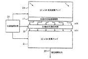
走査装置10には、少なくとも1つの航行センサ24又は26が含まれている。好適な実施例の場合、該装置には、1対の航行センサが含まれ、これらのセンサは、撮像センサ22の対向端に配置される。互いに直交して装着される光電素子の1次元アレイを利用することができるが、更に好適な実施例の場合、各航行センサは、光電素子の2次元アレイである。航行センサ24及び26を用いて、原稿に対する走査装置10の移動が追跡される。
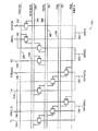
図4は、光電素子回路の概略図である。図5は、光電素子対の更に詳細な回路図である。入射光は、サンプル期間中に積分される電流へと変換される。記憶値は、処理シーケンスにおける次のステップに利用することができるように、周期的に読み出される。積分サイクルの開始時に、図4におけるリセット・スイッチ28が「オン」になり、瞬間的に積分コンデンサ30を3.25ボルトにリセットする。図5に示すように、リセット・スイッチ28は、pチャネル・トランジスタであり、第1のリセット線32を介してトランジスタのゲートに論理低を加えることによって「オン」となる。フォトダイオード34によって発生する光電流は、PNPトランジスタ36によって増幅される。フォトダイオード及びトランジスタは、寄生容量38と共に、光電素子40を規定する。増幅された光電流は、トランジスタ52を介して、1.75ボルトのレベルに向かう下方へと積分コンデンサ30を充電する。サンプル期間の終了時には、読み出しスイッチ42が「オン」になり、記憶値が、読み出し線44に沿って転送増幅器46に出力される。図5に示すように、読み出しスイッチは、nチャネル・トランジスタであり、読み出し制御線48によって制御される。
図4を参照して、特定の列転送増幅器46の基本動作について説明する。転送増幅器が読み出しモードにない場合、読み出し線44は、増幅器の第2の入力74に対して分路される。すなわち、2つの入力が、1.75ボルトに保持される。同時に、出力線108が、第2の定電圧源に接続される。重要ではないが、出力線108における電圧は3.25ボルトである。積分コンデンサ30も、リセット・スイッチ28によって3.25ボルトに接続される。
ここで、out は、転送動作の終了時における転送増幅器の出力電圧であり、Voutは、出力線108における開始電圧(すなわち、3.25ボルト)であり、Vcapは、積分コンデンサ用の開始電圧(すなわち、3.25ボルト)であり、Iph は、フォトダイオード電流(すなわち、0.6nA)であり、βは、フォトトランジスタ36の電流増幅率(すなわち18)であり、Tintは、受光装置のための積分時間(すなわち、40μs)であり、Cintは、積分コンデンサの値(すなわち、0.2pF)であり、Vbott は、転送増幅器の第2の入力74におけるバイアス値(すなわち、1.75ボルト)であり、Ctran は、転送コンデンサの値(すなわち、0.4pF)である。
次に図7を参照すると、列転送増幅器46が示されており、これは、4つのトランジスタ素子78、80、82、及び84によって、選択的に共に分路される第1の入力74と第2の入力76を備える。これらのトランジスタのうちの2つはスイッチとして機能し、一方、他の2つは、ある程度の電荷注入補償を与える。トランジスタ素子のスイッチングは、TRNRST線86における信号によって制御される。線86上の信号が論理高の場合、入力74及び76は、両方とも、VBB3線88を介して定電圧源に接続される。上例の場合、VBB3電圧は、1.75ボルトである。インバータ110及び112が、トランジスタ78−84に適正な信号レベルを供給する。
図3の計算アレイ21を介した光電素子の航行アレイ24からの信号処理における問題には、光電素子の近隣内で共通である特性の結果として、処理が潜在的に損なわれることが伴う。例えば、スキャナは、原稿に対して移動する際に、基体を照射するための光源を備える。照度にばらつきがなく、全視野領域を照射するのは困難である。信号処理は、こうしたばらつきによって悪影響を受ける可能性がある。
同様に、第2の差動セル262は、下記に等しい電流(Ix)を発生する。
第2の差動セルには、図11に帰還線298として簡単に示される負帰還が含まれるので、電流Ixは、強制的に−Iyになる。従って、DC除去が許可されると、以下のようになる。
式(3)は、次のように書き直すことができる。
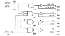
相互コンダクタンスgmxは、8つのトランジスタのバンク300によって変調される。バンク内のトランジスタのうちの4つが、三極管領域で、電圧GAINADJによりバイアスされて、トランジスタ264及び266の差動対に対する利得縮退抵抗器として機能する。バンク300内の他の4つのトランジスタは、利得縮退の抵抗性トランジスタに選択的に分路するためのスイッチとして利用され、G1及びG2デジタル利得制御入力の制御下にある。G1及びG2電圧は、図3に示す制御論理回路25によって設定される。

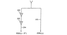
図17の回路は、F2動作モードを実施するために用いられる。図12及び17の共通線は、同じ参照番号によって識別される。図17の回路は、線192の一次入力及び線188の二次入力の一方に関して同じままである。しかし、線294における二次入力は、線192における一次入力と同じ転送増幅器からのものである。この入力は、同じ列からのものであるが、2τの遅延の結果、二次入力は異なる行からのものになる。好適には、遅延τは、転送増幅器のサンプリング時間に等しい。
増幅器の出力が、トランジスタ322を介してOFST_CTRLノードに接続されると、新たな負帰還経路が導入される。OFST_CTRLノードから増幅器出力への利得は、慣用的な入力から出力への利得の約100分の1になるので、トランジスタ322によって形成される一時的な負帰還経路によって、入力オフセットの100倍に等しい信号が、OFST_CTRLとバイアス電圧VBPの間に生じることになる。
前記差動回路が、読み出し動作からリセット動作に切り換えられる場合、前記第1の回路入力を前記第2の回路入力に接続するステップと、
前記差動回路が、前記読み出し動作から前記リセット動作に切り換えられる場合、前記回路出力を固定電圧状態の電源に接続するステップと、
前記リセット動作の第1の時間セグメントの後に続いて、前記電源から前記回路出力を切断し、それによって、前記回路出力が、前記固定電圧状態から自由に浮動する、前記リセット動作の第2の時間セグメントを開始するステップと、
前記第2の時間セグメントの間に、前記回路出力における電圧状態のシフトに応答して、オフセット補正信号を形成するステップと、
を含むことを特徴とする方法。
光電素子が、計算回路への光電流信号の転送に関して、動作的にグループ化され、それにより、複数の光電素子グループを規定する光電素子アレイと、
各転送増幅器が、1つの光電素子グループと動作的に関連するように、前記光電素子グループと1対1の対応を有する、複数の転送増幅器であって、各転送増幅器は、第1の入力及び第2の入力を備え、また該第1の入力と第2の入力の電圧状態の差を表す出力を備え、前記第2の入力は、基準電圧源に接続されている、複数の転送増幅器と、
前記グループ内の前記光電素子を、前記グループが動作的に関連している前記転送増幅器の前記第1の入力に順次接続し、また、前記光電素子のどれも前記入力に接続されていないリセット期間を与えるための、各光電素子グループに対する第1のスイッチング手段と、
前記第1と第2の入力における電圧状態が等しい前記リセット期間中に、前記第1の入力を前記第2の入力に接続するための、各転送増幅器に対する第2のスイッチング手段と、
前記リセット期間の少なくともいくつかの第1の部分の間、前記出力をリセット電圧源に接続し、また、前記リセット期間の第2の部分の間、前記出力を前記リセット電圧源から切断するための、各転送増幅器に対する第3のスイッチング手段と、
各転送増幅器に対する、前記出力への前記第1の入力の容量性結合と、
前記時間期間の1つの第2の部分の間、前記リセット電圧と、前記転送増幅器の前記出力の1つにおける電圧状態との間の電圧差の検出に応答して、前記転送増幅器にオフセット調整信号を供給するためのオフセット手段と、
からなる受光装置アレイ。
前記回路構成の各々が1つの出力を有する、複数の信号発生回路と、
該信号発生回路の前記出力から、空間周波数成分を除去するための複数のDC除去手段であって、各DC除去手段は、1つの特定の信号発生回路と動作的に関連しており、また前記特定の信号発生回路の出力から、問題となる信号を受信するように接続された一次入力を有し、前記各DC除去手段は、前記特定の信号発生回路に近接する前記信号発生回路の1つから出力された信号を受信するように接続された、少なくとも1つの二次入力を備え、前記各DC除去手段は、前記問題となる信号と、前記少なくとも1つの二次入力において受信された前記信号出力との間のアナログ信号差に応答して、1つの出力信号を供給するための差動手段を備える、複数のDC除去手段と、
からなる信号を転送するための回路構成。
12 経路
14 原稿
16 画像ディスプレイ
17 列転送増幅器
19 DC除去回路
21 計算アレイ
22 撮像センサ
24,26 航行センサ
25 制御論理回路
28 リセット・スイッチ
40 光電素子
42 読み出しスイッチ
46 転送増幅器
136 オフセット調整増幅器
148 サンプル/ホールド回路
198-206 スイッチング・ネットワーク
208-212 DC除去増幅器
260 第1の差動セルAy
262 第2の差動セルAx
Claims (7)
- 信号を転送するための回路構成において、
複数の信号生成回路(46、174、及び178)であって、前記回路の各々が出力(108、182、及び186)を有することからなる、複数の信号生成回路と、
前記回路の前記出力から低域の空間周波数成分を除去するための複数のDC除去手段(208、210、及び212)であって、DC除去手段の各々は、特定の回路と動作的に関連し、且つ、前記特定の回路の出力から対象とする信号を受信するために接続される一次入力部(230)を有し、且つ、前記特定の回路に近接する前記回路のうちの1つから信号出力を受信するために接続される、少なくとも1つの二次入力部(232及び234)を含み、且つ、前記対象とする信号と、前記二次入力部で受信された前記信号出力との間の差分のアナログ信号に応答する出力信号(236)を提供するための差動手段(260及び262)を含む、DC除去手段
を備える、回路構成。 - DC除去手段(208、210、及び212)の各々は、
前記一次入力部(230)と、前記少なくとも1つの二次入力部(232及び234)と、前記一次入力部と前記少なくとも1つの二次入力部との間の信号の差分に応答する出力ノード、とを有する第1の差動セル(260)と、
前記第1の差動セルの前記出力ノードに接続される第1の入力部と、第2の入力部(298)と、データ出力ノード(236)とを有する、第2の差動セル(262)であって、前記第2の入力部は、負帰還ループによって前記データ出力ノードに接続される、第2の差動セル(262)
を含む、請求項1の回路構成。 - 前記回路は、第1の行を形成するように配列された光電素子(40)であり、前記特定の回路は、前記第1の行の中の1つの光電素子であって、且つ、前記第1の行の中の中間の光電素子によって、前記少なくとも1つの二次入力(232及び234)に接続される全ての光電素子から隔置されることからなる、請求項1又は2の回路構成。
- DC除去手段(208、210、及び212)の各々は、前記第1の行の中の、異なる光電素子(40)と動作的に関連する、請求項3の回路構成。
- 光電素子の列(162、164、166、168、及び170)を画定するために、前記第1の行(40)と共に配列された光電素子の複数の第2の行(102)を含み、各々の前記DC除去手段は、光電素子の異なる列と動作的に関連する、請求項4の回路構成。
- 複数の信号生成回路(46、174、及び178)の個々の出力(108、182、及び186)に対してDC除去を提供する方法であって、
DC除去回路(208、210、及び212)を前記信号生成回路の各々に提供するステップと、
前記信号生成回路の各々の前記出力から、前記信号生成回路が提供される前記DC除去回路へ対象とする信号を提供するステップであって、前記対象とする信号を前記提供されたDC除去回路の一次入力部(230)に送るステップを含むことからなるステップと、
前記DC除去回路の各々の対応する数の二次入力部(232及び234)に少なくとも1つの二次信号を提供するステップであって、特定のDC除去回路への前記二次信号の各々は、前記特定のDC除去回路が提供される前記信号生成回路に近接する、前記信号生成回路のうちの1つの前記出力に応答することからなるステップと、
前記DC除去回路の各々から、DCが除去された信号を生成するステップであって、前記DCが除去された信号は、対象とする前記信号と、前記少なくとも1つの二次信号との間の差分のアナログ信号に応答することからなるステップ
を含む方法。 - 前記DC除去回路の各々を提供するステップは、前記DC除去回路を光電素子アレー中の特定の光電素子に接続するステップを含む、請求項6の方法。
Applications Claiming Priority (1)
| Application Number | Priority Date | Filing Date | Title |
|---|---|---|---|
| US08/591,076 US5703353A (en) | 1996-01-25 | 1996-01-25 | Offset removal and spatial frequency band filtering circuitry for photoreceiver signals |
Related Parent Applications (1)
| Application Number | Title | Priority Date | Filing Date |
|---|---|---|---|
| JP00082897A Division JP3956242B2 (ja) | 1996-01-25 | 1997-01-07 | 受光装置信号に対するオフセット除去及び空間周波数帯域フィルタリング回路及び方法 |
Publications (2)
| Publication Number | Publication Date |
|---|---|
| JP2004120801A true JP2004120801A (ja) | 2004-04-15 |
| JP4027308B2 JP4027308B2 (ja) | 2007-12-26 |
Family
ID=24364959
Family Applications (2)
| Application Number | Title | Priority Date | Filing Date |
|---|---|---|---|
| JP00082897A Expired - Lifetime JP3956242B2 (ja) | 1996-01-25 | 1997-01-07 | 受光装置信号に対するオフセット除去及び空間周波数帯域フィルタリング回路及び方法 |
| JP2003434480A Expired - Lifetime JP4027308B2 (ja) | 1996-01-25 | 2003-12-26 | 受光装置信号に対するオフセット除去及び空間周波数帯域フィルタリング回路及び方法 |
Family Applications Before (1)
| Application Number | Title | Priority Date | Filing Date |
|---|---|---|---|
| JP00082897A Expired - Lifetime JP3956242B2 (ja) | 1996-01-25 | 1997-01-07 | 受光装置信号に対するオフセット除去及び空間周波数帯域フィルタリング回路及び方法 |
Country Status (4)
| Country | Link |
|---|---|
| US (2) | US5703353A (ja) |
| EP (2) | EP1175090B1 (ja) |
| JP (2) | JP3956242B2 (ja) |
| DE (2) | DE69730367T2 (ja) |
Cited By (1)
| Publication number | Priority date | Publication date | Assignee | Title |
|---|---|---|---|---|
| KR100790259B1 (ko) | 2005-12-14 | 2008-01-02 | 매그나칩 반도체 유한회사 | 아날로그 디지털 컨버터, 이를 구비한 시모스 이미지 센서및 아날로그 옵셋 제거방법 |
Families Citing this family (26)
| Publication number | Priority date | Publication date | Assignee | Title |
|---|---|---|---|---|
| US6256016B1 (en) | 1997-06-05 | 2001-07-03 | Logitech, Inc. | Optical detection system, device, and method utilizing optical matching |
| US6025935A (en) * | 1997-12-31 | 2000-02-15 | Peripheral Imaging Corporation | Charge storage image scanner having equalizing pre-charge and reset improvements |
| US6233368B1 (en) * | 1998-03-18 | 2001-05-15 | Agilent Technologies, Inc. | CMOS digital optical navigation chip |
| US6002124A (en) * | 1998-03-20 | 1999-12-14 | Hewlett-Packard Company | Portable image scanner with optical position sensors |
| US6118132A (en) * | 1998-09-17 | 2000-09-12 | Agilent Technologies | System for measuring the velocity, displacement and strain on a moving surface or web of material |
| US6188058B1 (en) | 1998-09-17 | 2001-02-13 | Agilent Technologies Inc. | System for taking displacement measurements having photosensors with imaged pattern arrangement |
| US6304826B1 (en) * | 1999-02-05 | 2001-10-16 | Syscan, Inc. | Self-calibration method and circuit architecture of image sensor |
| US6246050B1 (en) | 1999-03-08 | 2001-06-12 | Hewlett-Packard Company | Optical encoders using non-patterned targets |
| US6633332B1 (en) * | 1999-05-13 | 2003-10-14 | Hewlett-Packard Development Company, L.P. | Digital camera system and method capable of performing document scans |
| US6362465B1 (en) | 1999-06-14 | 2002-03-26 | Hewlett-Packard Company | Optical scanning system and method capable of receiving inputs from a user |
| US6975355B1 (en) | 2000-02-22 | 2005-12-13 | Pixim, Inc. | Multiple sampling via a time-indexed method to achieve wide dynamic ranges |
| US6312124B1 (en) | 1999-10-27 | 2001-11-06 | Hewlett-Packard Company | Solid and semi-flexible body inkjet printing system |
| US6297984B1 (en) * | 1999-12-29 | 2001-10-02 | Tower Semiconductor Ltd. | Structure and method for protecting integrated circuits during plasma processing |
| US7161578B1 (en) | 2000-08-02 | 2007-01-09 | Logitech Europe S.A. | Universal presentation device |
| US7035932B1 (en) * | 2000-10-27 | 2006-04-25 | Eric Morgan Dowling | Federated multiprotocol communication |
| US6781570B1 (en) | 2000-11-09 | 2004-08-24 | Logitech Europe S.A. | Wireless optical input device |
| US6657487B2 (en) * | 2001-02-05 | 2003-12-02 | Em(Us) Design, Inc | Photodetector preamplifier circuit having a rotating input stage |
| US7333083B1 (en) | 2001-05-10 | 2008-02-19 | Logitech Europe S.A. | Optical based performance improvement for an optical illumination configuration |
| US6617565B2 (en) * | 2001-11-06 | 2003-09-09 | Omnivision Technologies, Inc. | CMOS image sensor with on-chip pattern recognition |
| US6788875B1 (en) | 2002-04-08 | 2004-09-07 | Logitech Europe S.A. | Suspension system for use in an optical displacement detection system |
| US7131751B1 (en) | 2002-04-12 | 2006-11-07 | Logitech, Inc. | Attachment system for use in an optical illumination system |
| US6876233B1 (en) | 2003-02-15 | 2005-04-05 | Medtronics, Inc. | DC cancellation apparatus and method |
| US7515188B2 (en) * | 2004-07-16 | 2009-04-07 | Micron Technology, Inc. | Method and system for reducing mismatch between reference and intensity paths in analog to digital converters in CMOS active pixel sensors |
| JP4978022B2 (ja) * | 2006-02-16 | 2012-07-18 | 富士通セミコンダクター株式会社 | 演算増幅器 |
| JP5495864B2 (ja) * | 2010-03-08 | 2014-05-21 | キヤノン株式会社 | 光電変換装置 |
| JP5360270B2 (ja) * | 2011-12-07 | 2013-12-04 | 凸版印刷株式会社 | 液晶表示装置 |
Family Cites Families (13)
| Publication number | Priority date | Publication date | Assignee | Title |
|---|---|---|---|---|
| US3937874A (en) * | 1975-01-09 | 1976-02-10 | General Electric Company | Offset voltage correction circuit for multiple video channel imager |
| US4409483A (en) * | 1980-10-07 | 1983-10-11 | Westinghouse Electric Corp. | Radiant energy differential sensor system |
| US4400729A (en) * | 1980-12-03 | 1983-08-23 | Jones George R | Pseudo-DC restore application to staring array detectors |
| DE3049043A1 (de) * | 1980-12-24 | 1982-07-15 | Robert Bosch Gmbh, 7000 Stuttgart | Verfahren und anordnung zur unterdrueckung des niederfrequenten rauschens bei ausgangssignalen von halbleiter- sensoren |
| JPS6152012A (ja) * | 1984-08-22 | 1986-03-14 | Hitachi Ltd | 差動増幅回路 |
| US4884039A (en) * | 1988-09-09 | 1989-11-28 | Texas Instruments Incorporated | Differential amplifier with low noise offset compensation |
| US4940981A (en) * | 1989-02-08 | 1990-07-10 | Burr-Brown Corporation | Dual analog-to-digital converter with single successive approximation register |
| JP2931088B2 (ja) * | 1990-11-30 | 1999-08-09 | キヤノン株式会社 | マルチチップ型光電変換装置 |
| US5149980A (en) * | 1991-11-01 | 1992-09-22 | Hewlett-Packard Company | Substrate advance measurement system using cross-correlation of light sensor array signals |
| JPH05219440A (ja) * | 1992-02-07 | 1993-08-27 | Olympus Optical Co Ltd | 画像入力装置 |
| JP2988795B2 (ja) * | 1992-05-29 | 1999-12-13 | シャープ株式会社 | 受光増幅装置 |
| US5352884A (en) * | 1993-04-14 | 1994-10-04 | General Electric Corporation | Method and apparatus for providing offset for light detector |
| FR2728420B1 (fr) * | 1994-12-16 | 1997-01-24 | Thomson Csf | Procede de compensation electronique des non-uniformites dans la detection d'images, en particulier infrarouge, et circuit de correction pour sa mise en oeuvre |
-
1996
- 1996-01-25 US US08/591,076 patent/US5703353A/en not_active Expired - Lifetime
-
1997
- 1997-01-07 JP JP00082897A patent/JP3956242B2/ja not_active Expired - Lifetime
- 1997-01-13 EP EP01117841A patent/EP1175090B1/en not_active Expired - Lifetime
- 1997-01-13 DE DE69730367T patent/DE69730367T2/de not_active Expired - Lifetime
- 1997-01-13 DE DE69737665T patent/DE69737665T2/de not_active Expired - Lifetime
- 1997-01-13 EP EP97300163A patent/EP0786899B1/en not_active Expired - Lifetime
- 1997-09-05 US US08/924,161 patent/US5900625A/en not_active Expired - Lifetime
-
2003
- 2003-12-26 JP JP2003434480A patent/JP4027308B2/ja not_active Expired - Lifetime
Cited By (1)
| Publication number | Priority date | Publication date | Assignee | Title |
|---|---|---|---|---|
| KR100790259B1 (ko) | 2005-12-14 | 2008-01-02 | 매그나칩 반도체 유한회사 | 아날로그 디지털 컨버터, 이를 구비한 시모스 이미지 센서및 아날로그 옵셋 제거방법 |
Also Published As
| Publication number | Publication date |
|---|---|
| JP4027308B2 (ja) | 2007-12-26 |
| US5703353A (en) | 1997-12-30 |
| EP0786899A3 (en) | 1998-10-14 |
| JPH10136149A (ja) | 1998-05-22 |
| US5900625A (en) | 1999-05-04 |
| DE69730367D1 (de) | 2004-09-30 |
| EP1175090A1 (en) | 2002-01-23 |
| EP0786899B1 (en) | 2004-08-25 |
| EP1175090B1 (en) | 2007-04-25 |
| JP3956242B2 (ja) | 2007-08-08 |
| DE69737665D1 (de) | 2007-06-06 |
| DE69737665T2 (de) | 2007-12-27 |
| EP0786899A2 (en) | 1997-07-30 |
| DE69730367T2 (de) | 2005-09-01 |
Similar Documents
| Publication | Publication Date | Title |
|---|---|---|
| JP3956242B2 (ja) | 受光装置信号に対するオフセット除去及び空間周波数帯域フィルタリング回路及び方法 | |
| US5769384A (en) | Low differential light level photoreceptors | |
| JP3581031B2 (ja) | 光検出装置 | |
| JP4277339B2 (ja) | アクティブ画素センサの読み出しチャネル | |
| JPH10256593A (ja) | アクティブインテグレータ・オプティカルセンサ用装置及び方法 | |
| JPH11287708A (ja) | 電気回路 | |
| JPH09233259A5 (ja) | ||
| US6952004B2 (en) | Image sensor with capacitive amplifier and associated methods | |
| JPH08149376A (ja) | 固体撮像装置 | |
| CN102905089A (zh) | 光电转换装置、焦点检测装置和成像系统 | |
| KR100959305B1 (ko) | 순차 판독 회로와 이를 포함하는 시스템 및 순차 판독 방법 | |
| US5917960A (en) | Image correlator, an image processing apparatus using the same, and a signal adder used in the image correlator | |
| US6104020A (en) | Electronic shutter for a low differential light level photo-receiver cell | |
| US10879856B2 (en) | Sensor array with distributed low noise amplifier | |
| US6649899B2 (en) | Systems and methods of sampling a photodetector and photocell circuits incorporating the same | |
| US6093924A (en) | Gain and error correction circuitry | |
| JP2000134410A (ja) | イメージセンサー | |
| EP0880851B1 (en) | Apparatus for reading and processing image information | |
| US20020097446A1 (en) | Apparatus and method for dark calibration of a linear CMOS sensor | |
| JPH1169231A (ja) | センサ出力読み出し回路 | |
| JPH08116491A (ja) | 光電変換装置 | |
| CN121691955A (zh) | 像素读出电路、控制像素读出电路的方法和感存算一体芯片 |
Legal Events
| Date | Code | Title | Description |
|---|---|---|---|
| A711 | Notification of change in applicant |
Free format text: JAPANESE INTERMEDIATE CODE: A711 Effective date: 20051028 |
|
| A977 | Report on retrieval |
Free format text: JAPANESE INTERMEDIATE CODE: A971007 Effective date: 20051107 |
|
| A131 | Notification of reasons for refusal |
Free format text: JAPANESE INTERMEDIATE CODE: A131 Effective date: 20051227 |
|
| A601 | Written request for extension of time |
Free format text: JAPANESE INTERMEDIATE CODE: A601 Effective date: 20060324 |
|
| A602 | Written permission of extension of time |
Free format text: JAPANESE INTERMEDIATE CODE: A602 Effective date: 20060329 |
|
| A521 | Request for written amendment filed |
Free format text: JAPANESE INTERMEDIATE CODE: A523 Effective date: 20060627 |
|
| A131 | Notification of reasons for refusal |
Free format text: JAPANESE INTERMEDIATE CODE: A131 Effective date: 20070403 |
|
| A521 | Request for written amendment filed |
Free format text: JAPANESE INTERMEDIATE CODE: A523 Effective date: 20070621 |
|
| A711 | Notification of change in applicant |
Free format text: JAPANESE INTERMEDIATE CODE: A711 Effective date: 20070727 |
|
| TRDD | Decision of grant or rejection written | ||
| A01 | Written decision to grant a patent or to grant a registration (utility model) |
Free format text: JAPANESE INTERMEDIATE CODE: A01 Effective date: 20070911 |
|
| A61 | First payment of annual fees (during grant procedure) |
Free format text: JAPANESE INTERMEDIATE CODE: A61 Effective date: 20071009 |
|
| FPAY | Renewal fee payment (event date is renewal date of database) |
Free format text: PAYMENT UNTIL: 20101019 Year of fee payment: 3 |
|
| R150 | Certificate of patent or registration of utility model |
Free format text: JAPANESE INTERMEDIATE CODE: R150 |
|
| FPAY | Renewal fee payment (event date is renewal date of database) |
Free format text: PAYMENT UNTIL: 20101019 Year of fee payment: 3 |
|
| S111 | Request for change of ownership or part of ownership |
Free format text: JAPANESE INTERMEDIATE CODE: R313113 |
|
| FPAY | Renewal fee payment (event date is renewal date of database) |
Free format text: PAYMENT UNTIL: 20101019 Year of fee payment: 3 |
|
| R360 | Written notification for declining of transfer of rights |
Free format text: JAPANESE INTERMEDIATE CODE: R360 |
|
| FPAY | Renewal fee payment (event date is renewal date of database) |
Free format text: PAYMENT UNTIL: 20101019 Year of fee payment: 3 |
|
| R350 | Written notification of registration of transfer |
Free format text: JAPANESE INTERMEDIATE CODE: R350 |
|
| FPAY | Renewal fee payment (event date is renewal date of database) |
Free format text: PAYMENT UNTIL: 20101019 Year of fee payment: 3 |
|
| S631 | Written request for registration of reclamation of domicile |
Free format text: JAPANESE INTERMEDIATE CODE: R313631 |
|
| S633 | Written request for registration of reclamation of name |
Free format text: JAPANESE INTERMEDIATE CODE: R313633 |
|
| R350 | Written notification of registration of transfer |
Free format text: JAPANESE INTERMEDIATE CODE: R350 |
|
| FPAY | Renewal fee payment (event date is renewal date of database) |
Free format text: PAYMENT UNTIL: 20101019 Year of fee payment: 3 |
|
| RD02 | Notification of acceptance of power of attorney |
Free format text: JAPANESE INTERMEDIATE CODE: R3D02 |
|
| FPAY | Renewal fee payment (event date is renewal date of database) |
Free format text: PAYMENT UNTIL: 20111019 Year of fee payment: 4 |
|
| S111 | Request for change of ownership or part of ownership |
Free format text: JAPANESE INTERMEDIATE CODE: R313113 |
|
| FPAY | Renewal fee payment (event date is renewal date of database) |
Free format text: PAYMENT UNTIL: 20111019 Year of fee payment: 4 |
|
| R350 | Written notification of registration of transfer |
Free format text: JAPANESE INTERMEDIATE CODE: R350 |
|
| FPAY | Renewal fee payment (event date is renewal date of database) |
Free format text: PAYMENT UNTIL: 20121019 Year of fee payment: 5 |
|
| FPAY | Renewal fee payment (event date is renewal date of database) |
Free format text: PAYMENT UNTIL: 20131019 Year of fee payment: 6 |
|
| R250 | Receipt of annual fees |
Free format text: JAPANESE INTERMEDIATE CODE: R250 |
|
| R250 | Receipt of annual fees |
Free format text: JAPANESE INTERMEDIATE CODE: R250 |
|
| R250 | Receipt of annual fees |
Free format text: JAPANESE INTERMEDIATE CODE: R250 |
|
| R250 | Receipt of annual fees |
Free format text: JAPANESE INTERMEDIATE CODE: R250 |
|
| EXPY | Cancellation because of completion of term |