JP2004134821A - 半導体装置 - Google Patents
半導体装置 Download PDFInfo
- Publication number
- JP2004134821A JP2004134821A JP2004031161A JP2004031161A JP2004134821A JP 2004134821 A JP2004134821 A JP 2004134821A JP 2004031161 A JP2004031161 A JP 2004031161A JP 2004031161 A JP2004031161 A JP 2004031161A JP 2004134821 A JP2004134821 A JP 2004134821A
- Authority
- JP
- Japan
- Prior art keywords
- resin
- semiconductor chip
- wiring board
- semiconductor device
- circuit wiring
- Prior art date
- Legal status (The legal status is an assumption and is not a legal conclusion. Google has not performed a legal analysis and makes no representation as to the accuracy of the status listed.)
- Granted
Links
Images







Classifications
-
- H—ELECTRICITY
- H10—SEMICONDUCTOR DEVICES; ELECTRIC SOLID-STATE DEVICES NOT OTHERWISE PROVIDED FOR
- H10W—GENERIC PACKAGES, INTERCONNECTIONS, CONNECTORS OR OTHER CONSTRUCTIONAL DETAILS OF DEVICES COVERED BY CLASS H10
- H10W70/00—Package substrates; Interposers; Redistribution layers [RDL]
- H10W70/60—Insulating or insulated package substrates; Interposers; Redistribution layers
- H10W70/67—Insulating or insulated package substrates; Interposers; Redistribution layers characterised by their insulating layers or insulating parts
- H10W70/68—Shapes or dispositions thereof
- H10W70/681—Shapes or dispositions thereof comprising holes not having chips therein, e.g. for outgassing, underfilling or bond wire passage
-
- H—ELECTRICITY
- H10—SEMICONDUCTOR DEVICES; ELECTRIC SOLID-STATE DEVICES NOT OTHERWISE PROVIDED FOR
- H10W—GENERIC PACKAGES, INTERCONNECTIONS, CONNECTORS OR OTHER CONSTRUCTIONAL DETAILS OF DEVICES COVERED BY CLASS H10
- H10W72/00—Interconnections or connectors in packages
- H10W72/071—Connecting or disconnecting
- H10W72/072—Connecting or disconnecting of bump connectors
-
- H—ELECTRICITY
- H10—SEMICONDUCTOR DEVICES; ELECTRIC SOLID-STATE DEVICES NOT OTHERWISE PROVIDED FOR
- H10W—GENERIC PACKAGES, INTERCONNECTIONS, CONNECTORS OR OTHER CONSTRUCTIONAL DETAILS OF DEVICES COVERED BY CLASS H10
- H10W72/00—Interconnections or connectors in packages
- H10W72/071—Connecting or disconnecting
- H10W72/072—Connecting or disconnecting of bump connectors
- H10W72/07251—Connecting or disconnecting of bump connectors characterised by changes in properties of the bump connectors during connecting
-
- H—ELECTRICITY
- H10—SEMICONDUCTOR DEVICES; ELECTRIC SOLID-STATE DEVICES NOT OTHERWISE PROVIDED FOR
- H10W—GENERIC PACKAGES, INTERCONNECTIONS, CONNECTORS OR OTHER CONSTRUCTIONAL DETAILS OF DEVICES COVERED BY CLASS H10
- H10W72/00—Interconnections or connectors in packages
- H10W72/071—Connecting or disconnecting
- H10W72/073—Connecting or disconnecting of die-attach connectors
-
- H—ELECTRICITY
- H10—SEMICONDUCTOR DEVICES; ELECTRIC SOLID-STATE DEVICES NOT OTHERWISE PROVIDED FOR
- H10W—GENERIC PACKAGES, INTERCONNECTIONS, CONNECTORS OR OTHER CONSTRUCTIONAL DETAILS OF DEVICES COVERED BY CLASS H10
- H10W72/00—Interconnections or connectors in packages
- H10W72/20—Bump connectors, e.g. solder bumps or copper pillars; Dummy bumps; Thermal bumps
-
- H—ELECTRICITY
- H10—SEMICONDUCTOR DEVICES; ELECTRIC SOLID-STATE DEVICES NOT OTHERWISE PROVIDED FOR
- H10W—GENERIC PACKAGES, INTERCONNECTIONS, CONNECTORS OR OTHER CONSTRUCTIONAL DETAILS OF DEVICES COVERED BY CLASS H10
- H10W72/00—Interconnections or connectors in packages
- H10W72/30—Die-attach connectors
- H10W72/381—Auxiliary members
- H10W72/387—Flow barriers
-
- H—ELECTRICITY
- H10—SEMICONDUCTOR DEVICES; ELECTRIC SOLID-STATE DEVICES NOT OTHERWISE PROVIDED FOR
- H10W—GENERIC PACKAGES, INTERCONNECTIONS, CONNECTORS OR OTHER CONSTRUCTIONAL DETAILS OF DEVICES COVERED BY CLASS H10
- H10W74/00—Encapsulations, e.g. protective coatings
- H10W74/10—Encapsulations, e.g. protective coatings characterised by their shape or disposition
- H10W74/15—Encapsulations, e.g. protective coatings characterised by their shape or disposition on active surfaces of flip-chip devices, e.g. underfills
Landscapes
- Wire Bonding (AREA)
- Encapsulation Of And Coatings For Semiconductor Or Solid State Devices (AREA)
Abstract
【構成】 回路配線基板と、この基板上にバンプ電極を介して実装された半導体素子とを具備し、前記回路配線基板と半導体素子との間隙および半導体素子の周囲に樹脂が配置された半導体装置である。前記バンプ電極は前記半導体素子の外周に沿って形成され、前記回路配線基板表面のバンプ電極で囲まれている領域内に凹部が形成されていることを特徴とする。
【選択図】 図11
Description
(Cは定数、fは周波数、Tmaxは最大温度である。)で表されるサイクル寿命の式から、バンプ部分に発生する最大剪断歪みγmax を減少させることにより信頼性寿命が向上することが知られている(IBM J.Res.Develop.,13;251(1969))。
(Dmin;最小バンプ径,β;材料定数,V;はんだ体積,h;はんだ高さ,Δα;熱膨張係数の差,ΔT;温度差,d;チップ中心からバンプ中心までの距離)
したがって、従来のフリップチップ実装技術においては、以下に挙げるような手段を用いてバンプ電極に発生する応力を低減させてきた。すなわち、(1)半導体チップの中心からバンプ電極の中心までの距離を小さくする、(2)半導体チップの熱膨張係数と回路配線基板の熱膨張係数との差を小さくする、(3)接続部の温度差が大きくならないように装置の放熱性を向上させる、(4)発生する応力歪みを充分に吸収できるように、バンプ電極の構造を改良する等の手段である。
図1に、参考例Iの半導体装置の断面図を示し、図2にこの装置の平面図を示す。
フィラ含有量(重量%) 30 45
平均粒径(μm) 5 10
最大粒径(μm) 20 35
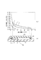
得られた半導体装置100個について、85℃,85%,VDD=5Vの高温高湿バイアス保存試験を行い、バンプ電極が1箇所でもオープンあるいはショートを発生した場合を不良として、保存時間と累積不良率との関係を調べ、図10中に曲線eで示した。
以下、図面を参照して、本発明の半導体装置を詳細に説明する。

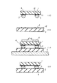
図15に、実施例IIの半導体装置の一例を表わす断面図を示す。
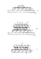
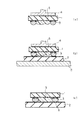
5…第1の樹脂,6…第2の樹脂,7…最外周バンプ電極の中心
8…Alボンディングパッド,9…半導体装置,10…バリアメタル
11…パッシベーション膜,12…ソルダーレジスト,13…ステージ
14…コレット,15…ディスペンサー,20…半導体装置,21…回路基板
22…接続電極,23…半導体チップ,24…接続電極,25…ハンダバンプ
26…樹脂,27…凹部,28…液体吐出装置,30…半導体装置,31…回路基板
32…接続電極,33…半導体チップ,34…接続電極,35…ハンダバンプ
36…樹脂,37…半導体装置,38…エポキシコーティング層,40…半導体装置
41…回路基板,42…接続電極,43…半導体チップ,44…接続電極
45…ハンダバンプ,46…樹脂,48…液体吐出装置,70…半導体装置
71…回路配線基板,72…半導体チップ,73…バンプ電極,74…接続用端子
75…接続用端子,77…半導体装置,78…従来の樹脂,80…半導体装置
81…間隙部分,83…回路基板,84…半導体チップ,85…バンプ電極
86…樹脂,87…気泡。
Claims (2)
- 回路配線基板と、この基板上にバンプ電極を介して実装された半導体素子とを具備し、前記回路配線基板と半導体素子との間隙および半導体素子の周囲に樹脂が配置された半導体装置において、
前記バンプ電極は前記半導体素子の外周に沿って形成され、前記回路配線基板表面のバンプ電極で囲まれている領域内に凹部が形成されていることを特徴とする半導体装置。 - 回路配線基板と、この基板上にバンプ電極を介して実装された半導体素子とを具備し、前記回路配線基板と半導体素子との間隙および半導体素子の周囲に樹脂が配置された半導体装置において、
前記樹脂は、室温で50ポイズ以下の粘度を有し、最大粒径が前記半導体素子と回路配線基板との距離の1/2以下の充填材を、20ないし70重量%の割合で含有し、前記間隙体積の1倍以上3倍以下の体積で配置されていることを特徴とする半導体装置。
Priority Applications (1)
| Application Number | Priority Date | Filing Date | Title |
|---|---|---|---|
| JP2004031161A JP3846890B2 (ja) | 2004-02-06 | 2004-02-06 | 半導体装置 |
Applications Claiming Priority (1)
| Application Number | Priority Date | Filing Date | Title |
|---|---|---|---|
| JP2004031161A JP3846890B2 (ja) | 2004-02-06 | 2004-02-06 | 半導体装置 |
Related Parent Applications (1)
| Application Number | Title | Priority Date | Filing Date |
|---|---|---|---|
| JP00351895A Division JP3648277B2 (ja) | 1995-01-12 | 1995-01-12 | 半導体装置 |
Publications (2)
| Publication Number | Publication Date |
|---|---|
| JP2004134821A true JP2004134821A (ja) | 2004-04-30 |
| JP3846890B2 JP3846890B2 (ja) | 2006-11-15 |
Family
ID=32291504
Family Applications (1)
| Application Number | Title | Priority Date | Filing Date |
|---|---|---|---|
| JP2004031161A Expired - Fee Related JP3846890B2 (ja) | 2004-02-06 | 2004-02-06 | 半導体装置 |
Country Status (1)
| Country | Link |
|---|---|
| JP (1) | JP3846890B2 (ja) |
Cited By (4)
| Publication number | Priority date | Publication date | Assignee | Title |
|---|---|---|---|---|
| JP2008103450A (ja) * | 2006-10-18 | 2008-05-01 | Matsushita Electric Ind Co Ltd | モジュールの製造方法 |
| JP2009071155A (ja) * | 2007-09-14 | 2009-04-02 | Fujitsu Ltd | 半導体装置およびその製造方法 |
| JP2012124238A (ja) * | 2010-12-07 | 2012-06-28 | Namics Corp | 電子部品実装体、および電子部品の実装方法 |
| CN111584435A (zh) * | 2020-05-14 | 2020-08-25 | 南通通富微电子有限公司 | 基板、芯片封装结构及其制备方法 |
-
2004
- 2004-02-06 JP JP2004031161A patent/JP3846890B2/ja not_active Expired - Fee Related
Cited By (5)
| Publication number | Priority date | Publication date | Assignee | Title |
|---|---|---|---|---|
| JP2008103450A (ja) * | 2006-10-18 | 2008-05-01 | Matsushita Electric Ind Co Ltd | モジュールの製造方法 |
| JP2009071155A (ja) * | 2007-09-14 | 2009-04-02 | Fujitsu Ltd | 半導体装置およびその製造方法 |
| JP2012124238A (ja) * | 2010-12-07 | 2012-06-28 | Namics Corp | 電子部品実装体、および電子部品の実装方法 |
| CN111584435A (zh) * | 2020-05-14 | 2020-08-25 | 南通通富微电子有限公司 | 基板、芯片封装结构及其制备方法 |
| CN111584435B (zh) * | 2020-05-14 | 2023-11-24 | 南通通富微电子有限公司 | 基板、芯片封装结构及其制备方法 |
Also Published As
| Publication number | Publication date |
|---|---|
| JP3846890B2 (ja) | 2006-11-15 |
Similar Documents
| Publication | Publication Date | Title |
|---|---|---|
| JP3648277B2 (ja) | 半導体装置 | |
| JP4534062B2 (ja) | 半導体装置 | |
| US7816780B2 (en) | Semiconductor apparatus and manufacturing method of semiconductor apparatus | |
| US7300865B2 (en) | Method for bonding IC chips to substrates incorporating dummy bumps and non-conductive adhesive | |
| US6373142B1 (en) | Method of adding filler into a non-filled underfill system by using a highly filled fillet | |
| US5864178A (en) | Semiconductor device with improved encapsulating resin | |
| US8338287B2 (en) | Semiconductor device and method for manufacturing the same | |
| US6387794B2 (en) | Electrode structure for semiconductor device, method for forming the same, mounted body including semiconductor device and semiconductor device | |
| CN101207100A (zh) | 半导体器件及其制造方法 | |
| US6605491B1 (en) | Method for bonding IC chips to substrates with non-conductive adhesive | |
| JP4206631B2 (ja) | 熱硬化性液状封止樹脂組成物、半導体素子の組立方法及び半導体装置 | |
| US6281571B1 (en) | Semiconductor device having an external connection electrode extending through a through hole formed in a substrate | |
| US20090017582A1 (en) | Method for manufacturing semiconductor device | |
| JP3454977B2 (ja) | 半導体装置及びその製造方法 | |
| JP4089531B2 (ja) | 半導体装置の製造方法 | |
| JP2003258034A (ja) | 多層配線基体の製造方法および多層配線基体 | |
| JPH10294337A (ja) | 半導体装置及びその製造方法 | |
| JP3846890B2 (ja) | 半導体装置 | |
| JP2003100810A (ja) | 半導体装置とその製造方法 | |
| JP6123836B2 (ja) | 半導体装置の製造方法 | |
| JP2000290471A (ja) | 封止用樹脂組成物 | |
| JP5245270B2 (ja) | 半導体装置及びその製造方法 | |
| JPH09172110A (ja) | 半導体装置 | |
| JP2000036506A (ja) | 半導体装置の製法 | |
| JP3951903B2 (ja) | 半導体装置及び半導体装置実装体の製造方法 |
Legal Events
| Date | Code | Title | Description |
|---|---|---|---|
| A621 | Written request for application examination |
Free format text: JAPANESE INTERMEDIATE CODE: A621 Effective date: 20040206 |
|
| A131 | Notification of reasons for refusal |
Free format text: JAPANESE INTERMEDIATE CODE: A131 Effective date: 20060131 |
|
| A521 | Request for written amendment filed |
Free format text: JAPANESE INTERMEDIATE CODE: A523 Effective date: 20060403 |
|
| A02 | Decision of refusal |
Free format text: JAPANESE INTERMEDIATE CODE: A02 Effective date: 20060425 |
|
| A521 | Request for written amendment filed |
Free format text: JAPANESE INTERMEDIATE CODE: A523 Effective date: 20060626 |
|
| A911 | Transfer to examiner for re-examination before appeal (zenchi) |
Free format text: JAPANESE INTERMEDIATE CODE: A911 Effective date: 20060719 |
|
| TRDD | Decision of grant or rejection written | ||
| A01 | Written decision to grant a patent or to grant a registration (utility model) |
Free format text: JAPANESE INTERMEDIATE CODE: A01 Effective date: 20060818 |
|
| A61 | First payment of annual fees (during grant procedure) |
Free format text: JAPANESE INTERMEDIATE CODE: A61 Effective date: 20060821 |
|
| FPAY | Renewal fee payment (event date is renewal date of database) |
Free format text: PAYMENT UNTIL: 20090901 Year of fee payment: 3 |
|
| FPAY | Renewal fee payment (event date is renewal date of database) |
Free format text: PAYMENT UNTIL: 20100901 Year of fee payment: 4 |
|
| FPAY | Renewal fee payment (event date is renewal date of database) |
Free format text: PAYMENT UNTIL: 20110901 Year of fee payment: 5 |
|
| FPAY | Renewal fee payment (event date is renewal date of database) |
Free format text: PAYMENT UNTIL: 20110901 Year of fee payment: 5 |
|
| FPAY | Renewal fee payment (event date is renewal date of database) |
Free format text: PAYMENT UNTIL: 20120901 Year of fee payment: 6 |
|
| LAPS | Cancellation because of no payment of annual fees |