JP2004198747A - Liquid crystal display - Google Patents
Liquid crystal display Download PDFInfo
- Publication number
- JP2004198747A JP2004198747A JP2002367403A JP2002367403A JP2004198747A JP 2004198747 A JP2004198747 A JP 2004198747A JP 2002367403 A JP2002367403 A JP 2002367403A JP 2002367403 A JP2002367403 A JP 2002367403A JP 2004198747 A JP2004198747 A JP 2004198747A
- Authority
- JP
- Japan
- Prior art keywords
- control signal
- gate
- liquid crystal
- voltage application
- application time
- Prior art date
- Legal status (The legal status is an assumption and is not a legal conclusion. Google has not performed a legal analysis and makes no representation as to the accuracy of the status listed.)
- Withdrawn
Links
Images

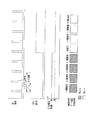


Landscapes
- Liquid Crystal (AREA)
- Liquid Crystal Display Device Control (AREA)
- Control Of Indicators Other Than Cathode Ray Tubes (AREA)
Abstract
【課題】TFTの電気的特性(電圧−電流特性)に僅かなずれが場合でも容易および確実に不良品検出を行う。
【解決手段】液晶パネル20の設けられている各TFT25に対して、通常動作用のゲート制御信号の電圧印加時間である駆動電圧印加時間および電気的特性検査用のゲート制御信号の電圧印加時間である駆動電圧印加時間(例えば、それぞれ50μsecおよび30μsec)を切換えて画像表示させるので、TFT25の電気的特性不良の場合には、所定切換時間(nフィールド期間)毎に表示画像の輝度の濃淡により、TFT25の電気的特性の僅かなシフトによる不良品をも容易かつ確実に確認可能となり、従来のように検査対象装置と基準となる比較対象装置とを共に動作させて大規模な装置で時間をかけて表示画像の輝度を比較する必要がなくなる。
【選択図】 図1An object of the present invention is to easily and surely detect a defective product even when a slight shift occurs in electrical characteristics (voltage-current characteristics) of a TFT.
Kind Code: A1 A drive voltage application time, which is a voltage application time of a gate control signal for normal operation, and a voltage application time of a gate control signal for electrical characteristic inspection, for each TFT 25 provided on a liquid crystal panel 20. Since an image is displayed by switching a certain drive voltage application time (for example, 50 μsec and 30 μsec, respectively), when the electrical characteristics of the TFT 25 are defective, the brightness of the display image is changed every predetermined switching time (n-field period). Defective products due to slight shifts in the electrical characteristics of the TFT 25 can be easily and reliably confirmed, and it takes time with a large-scale device to operate both the device to be inspected and the device to be compared as a conventional device. This eliminates the need to compare the brightness of the displayed image.
[Selection diagram] Fig. 1
Description
【0001】
【発明の属する技術分野】
本発明は、TFT(Thin Film Transistor)の電圧−電流特性等の電気的特性のずれを検出する電気的特性検出回路が搭載されたアクティブマトリックス型液晶表示装置等の液晶表示装置に関する。
【0002】
【従来の技術】
絶縁性基板上に複数の絵素電極をマトリクス状に配置し、各絵素電極に独立して映像信号を印加するアクティブマトリクス方式は、液晶テレビジョン、携帯電話、コンピュータの端末表示装置等の表示装置に実用化されている。
【0003】
図11は、従来のアクティブマトリックス型液晶表示装置の要部の構成の一例を示すブロック図である。
【0004】
図11に示すアクティブマトリックス型液晶表示装置100は、表示画面が設けられている液晶表示パネル200と、映像信号を液晶表示パネル200に供給する映像信号線駆動手段であるソースドライバ300と、映像信号を液晶表示パネル200に供給するタイミングを制御する制御信号線駆動手段であるゲートドライバ400と、これらのソースドライバ300およびゲートドライバ400に対して同期制御信号を供給する制御IC500とを有している。
【0005】
制御IC500は、シリアル信号SIが入力されるシリアルパラレル変換回路501と、シリアルパラレル変換回路501からの制御信号によってゲートクロック信号CLGを発生させるCLG発生回路502とを有しており、入力サンプリング信号SP、クロック信号CLKおよび転送信号TRSをソースドライバ300に出力し、スタートパルス信号SPGおよびゲートクロック信号CLGをゲートドライバ400に出力する。
【0006】
ソースドライバ300は、制御IC500からの入力サンプリング信号SPおよびクロック信号CLKが入力され、入力サンプリング信号SPをクロック信号CLKに同期させて、順次遅延させたサンプリング信号を順次出力するHシフトレジスタ301と、RGB信号入力端子Sinを介して映像信号の各色成分であるRGB信号が入力されるRGB信号線302と、Hシフトレジスタ301からのサンプリング信号によりRGB信号線302からのRGB信号の各色信号を選択し、オン/オフ動作を繰り返して順次RGB信号のそれぞれの色信号を出力する複数のサンプリングSW(スイッチ)303と、サンプリングSW303を介してRGB信号線302から供給されるRGB信号の各色信号をそれぞれ一旦保持する複数のサンプリングコンデンサ304と、制御IC500からの転送信号TRSを印加されることによりオン状態となり各サンプリングコンデンサ304にそれぞれ保持されたRGB信号の各色信号を一斉に転送する複数の転送SW(スイッチ)305と、各転送SW305を介して各サンプリングコンデンサ304から転送されたRGB信号の各色信号をそれぞれ一旦保持する複数の転送コンデンサ306と、各転送コンデンサ306にそれぞれ保持されたRGB信号の各色信号を増幅して複数の映像信号線204にそれぞれ出力する複数のオペアンプ307とを有している。
【0007】
ここで、サンプリングコンデンサ304および転送コンデンサ306は、それぞれサンプリングSW303および転送SW305の出力端子とアース(GND)との間にそれぞれ接続され、RGB信号の各色信号は、それぞれオペアンプ307の非反転入力端子(+)に入力され、オペアンプ307の反転入力端子(−)および出力端子は短絡されている。そして、各オペアンプ307の出力端子は、それぞれの映像信号線204に接続されている。
【0008】
ゲートドライバ400は、制御IC500からの入力スタートパルス信号SPGを、制御IC500から出力されるゲートクロック信号CLGに同期させて、順次遅延させたゲート制御信号線選択信号を順次出力するVシフトレジスタ401と、外部供給電圧端子VGHを介して外部供給電圧のゲート電圧VGH1が印加される複数の出力バッファ402とを有している。出力バッファ402は、P型MOSトランジスタ402aおよびN型MOSトランジスタ402bから構成されたインバータ回路である。P型MOSトランジスタ402aのドレイン端子およびゲート端子は、それぞれN型MOSトランジスタ402bのドレイン端子およびゲート端子にそれぞれ接続される。P型MOSトランジスタ402aおよびN型MOSトランジスタ402bの各ドレイン端子は、出力バッファ402の出力端子となりゲート制御信号線203に接続されている。P型MOSトランジスタ402aおよびN型MOSトランジスタ402bの各ゲート端子は、出力バッファ402の入力端子となる。出力バッファ402の入力端子には、Vシフトレジスタ401から出力されるゲート制御信号線選択信号が入力される。P型MOSトランジスタ402aおよびN型MOSトランジスタ402bのソース端子は、それぞれ外部供給電圧端子VGHおよびアース(GND)に接続される。
【0009】
出力バッファ402は、Vシフトレジスタ401からのゲート制御信号線選択信号によって、オン/オフ動作を行い出力端子よりゲート制御信号線203にゲート制御信号であるゲート電圧VGH1を出力する。出力バッファ402は、ゲート制御信号線203毎に設けられている。
【0010】
液晶表示パネル200は、マトリクス状に配置された複数の絵素電極201を有するガラス板等の透明絶縁性基板(以下、アクティブマトリクス基板と記載する)と、このアクティブマトリクス基板に対向して配設され、膜状の共通(対向)電極202が設けられたガラス板等の透明絶縁性基板(以下、対向基板と記載する)とを有し、アクティブマトリクス基板と対向基板との間には、液晶層LCが挟持されている。
【0011】
アクティブマトリクス基板は、走査線として機能する複数のゲート制御信号線203(ゲート信号線)と、これらのゲート制御信号線203と直交し、信号線として機能する複数の映像信号線204(ソース信号線)とを有している。各ゲート制御信号線203および各映像信号線204の直交する位置の近傍には、絵素電極駆動素子205がそれぞれ配置されている。絵素電極駆動素子205のゲート端子およびソース端子は、それぞれゲート制御信号線203および映像信号線204にそれぞれ接続されており、絵素電極駆動素子205の駆動端子であるドレイン端子は、絵素電極201に接続されている。各絵素電極201は、それぞれのゲート制御信号線203および映像信号線204に囲まれた領域に設けられている。
【0012】
絵素電極駆動素子(以下、TFTと記載する)205には、アモルファスシリコンによって形成された薄膜トランジスタ(TFT:Thin Film Transister)、MIM(Metal Insulator Metal)素子等が用いられる。
【0013】
図11に示す液晶表示装置は、このような構成により、まず、RGB信号入力端子Sinを介して映像信号の各色成分であるRGB信号が、ソースドライバ300に設けられているRGB信号線302に入力される。同時に、Hシフトレジスタ301は、入力サンプリング信号SPおよびクロック信号CLKが入力され、入力サンプリング信号SPをクロック信号CLKに同期させて、順次遅延させたサンプリング信号を順次サンプリングSW(スイッチ)303に出力する。この時、RGB信号線302における1水平期間の映像信号の各色信号が、液晶表示パネル200に表示すべき映像信号として各サンプリングSW303にて順次サンプリングされ、このサンプリングされた映像信号の各色成分が各サンプリングコンデンサ304に順次保持される。
【0014】
次に、上記サンプリング動作までの間に、制御IC500から出力される転送信号TRSによって各転送SW305がオン状態となり、1水平期間の映像信号は、保持された各サンプリングコンデンサ304から各転送SW305をそれぞれ介して各転送コンデンサ306にそれぞれ転送される。さらに、各転送コンデンサ304に充電された各映像信号出力電圧は各オペアンプ307によってそれぞれ増幅された後に各映像信号線204にそれぞれ転送される。
【0015】
一方、各映像信号線204にそれぞれ出力された1水平期間の映像信号は、ゲートドライバ400の出力バッファ402から各ゲート制御信号線203にそれぞれ順次出力されるゲート制御信号によって、所定のゲート制御信号線203に接続される1ライン(走査)分の横一列の複数のTFT205が一斉にオン状態となり、複数の映像信号線204上の各映像信号電圧がそれぞれ、各TFT205のドレイン端子を通して各絵素電極201にそれぞれ書き込まれる。
【0016】
この場合のゲートドライバ400の出力バッファ402から出力されるゲート制御信号の出力タイミングについて説明する。
【0017】
図12は、図11に示すゲートドライバ400の各出力バッファ402から出力されるそれぞれのゲート制御信号のタイミングチャートである。
【0018】
図12に示すように、ゲートドライバ400のVシフトレジスタ401では、制御IC500から出力されたスタートパルス信号SPGが入力されると、制御IC500から出力された所定周波数のゲートクロック信号CLGに同期して、ゲート制御信号線選択信号が出力バッファ402に出力され、ゲート制御信号線選択信号に基づいて出力バッファ402からゲート制御信号であるゲート電圧VGH1がゲート制御信号線204に出力される。例えば、液晶表示パネル200の画面1行目(第1ライン目)のゲート制御信号線203に対して、この第1ライン目のゲート制御信号線203に対応する出力バッファ402よりゲート制御信号であるゲート電圧VGH1が出力され、このゲート制御信号によって液晶表示パネル200の画面1行目が表示される。さらに、所定周波数のゲートクロック信号CLGに同期して、画面2行目(第2ライン目)のゲート制御信号線204に対して、この第2ライン目のゲート制御信号線203に対応する出力バッファ402よりゲート制御信号が出力され、このゲート制御信号によって液晶表示パネル200の画面2行目が表示される。出力バッファ402よりゲート制御信号が出力される動作は、所定周波数のゲートクロック信号CLGの周期で繰り返されて、1垂直期間内での1画面が表示される。尚、出力バッファ402からゲート制御信号線203に出力されるゲート制御信号であるゲート電圧VGH1は、HIGH状態ではVGH(HIGH)=13V、LOW状態ではVGH(LOW)=0V(GND)である。
【0019】
【発明が解決しようとする課題】
しかしながら、従来の液晶表示装置100では、ゲート電圧VGH1のHIGH状態の期間が一定であってもTFT205の電圧−電流特性等の電気的特性が不良である場合には、映像信号の信号レベルが正確に絵素電極201に書き込まれない(充電不足)おそれがある。
【0020】
従来のTFTの電気的特性の検査方法では、液晶表示装置100において、TFTによる絵素電極201の充電不足か否かを判定するために、液晶層LCに印加する映像信号電圧を固定値とし、電気的特性が良好なTFTで形成された液晶表示装置100の輝度を基準として定め、検査対象の液晶表示装置100の輝度を測定し、基準の液晶表示装置100の輝度と検査対象の液晶表示装置100の輝度とを比較することにとって、TFTに対して良品または不良品かを判定している。
【0021】
この場合に、測定される検査対象の液晶表示装置100と比較するために、良品のTFTで形成された、基準となる液晶表示装置100も輝度を確認するために画像を表示させる必要がある。
【0022】
これにより、検査対象の液晶表示装置100の輝度測定とともに、比較対象の良品のTFTで形成された、基準となる液晶表示装置100の輝度を測定する時間が必要となり、処理スピードが低下する大きな要因になっている。そして、良品のTFTで形成された、基準となる液晶表示装置100と検査対象の液晶表示装置100とを比較する場合において、検査装置の規模が大きくなるとともに、比較用の良品のTFTで形成された基準となる液晶表示装置100を駆動させる駆動回路も必要となり、TFTの電気的特性の検査におけるコストアップにつながっている。
【0023】
また、TFTの電気的特性が検査された液晶表示装置100が出荷された後に、液晶表示装置100が使用された各種製品の製造工程および運搬時に、静電気などによってTFTの電気的特性がわずかにシフトする場合がある。この場合、従来の液晶表示装置100におけるTFTの電気的特性の検査方法では、TFTの電気的特性が極端なシフトであれば不良品として判定が可能であるが、TFTの電気的特性が僅かなシフトであれば不良品としての判定が難しく、検出されないおそれがある。
【0024】
上記の問題点のある従来のTFTの電気的特性の良否判定を行う検査方法において、本発明者等は、TFTの電気的特性について以下のように検討した。
【0025】
図13は、図11に示すソースドライバ300のオペアンプ307から出力される映像信号出力電圧、制御IC500からのゲートクロック信号CLGに同期するTFTのゲート電圧およびドレイン電圧のタイミングチャートである。
【0026】
図13において、各信号波形について順次説明する。
【0027】
まず、ソースドライバ300のオペアンプ307からの映像信号出力電圧の出力信号波形において、映像信号出力電圧の期間(a)は、HIGHレベル電圧の映像信号を絵素電極201に書き込むタイミングであり、次の期間(b)は、LOWレベル電圧の映像信号を絵素電極201に書き込むタイミングである。
【0028】
また、ゲートクロック信号CLG(1)および(2)のHIGHレベル電圧によって、ゲートドライバ400の出力バッファ402から出力されるゲート制御信号がHIGHレベル電圧になってTFTのゲートGをオン状態にし、ゲートクロック信号CLG(1)および(2)のLOWレベル電圧によって、ゲートドライバ400の出力バッファ402から出力されるゲート制御信号がLOWレベル電圧となりTFTのゲートGをオフ状態にする。ここで、ゲートクロック信号CLG(1)および(2)の信号波形の相違は、それぞれHIGHレベル状態の期間(ON期間)が50μsおよび30μsの違いである。
【0029】
次に、TFTのドレインDの出力信号波形(イ)は、映像信号出力電圧が期間(a)の状態において、ゲートクロック信号CLG(1)のHIGHレベルのタイミング(ゲート電圧のHIGHレベルのタイミング)で正常なTFT(良品)を介して、ソースドライバ300から出力される最大電圧5Vの映像信号を絵素電極201に書き込む場合の信号波形を示している。
【0030】
次に、TFTのドレインDの出力信号波形(イ’)は、映像信号出力電圧が期間(a)の状態において、ゲートクロック信号CLG(2)のHIGHレベルのタイミング(ゲート電圧のHIGHレベルのタイミング)で正常なTFT(良品)を介して、ソースドライバ300から出力される最大電圧5Vの映像信号を絵素電極201に書き込む場合の信号波形を示している。
【0031】
次に、TFTのドレインDの出力信号波形(ロ)は、映像信号出力電圧が期間(b)の状態において、ゲートクロック信号CLG(1)のHIGHレベルのタイミング(ゲート電圧のHIGHレベルのタイミング)で正常なTFT(良品)を介して、ソースドライバ300から出力される最小電圧1Vの映像信号を絵素電極201に書き込む場合の信号波形を示している。
【0032】
次に、TFTのドレインDの出力信号波形(ロ’)は、映像信号出力電圧が期間(b)の状態において、ゲートクロック信号CLG(2)のHIGHレベルのタイミング(ゲート電圧のHIGHレベルのタイミング)で正常なTFT(良品)を介して、ソースドライバ300から出力される最小電圧1Vの映像信号を絵素電極201に書き込む場合の信号波形を示している。
【0033】
次に、TFTのドレインDの出力信号波形(ハ)は、映像信号出力電圧が期間(a)の状態において、ゲートクロック信号CLG(1)のHIGHレベルのタイミング(ゲート電圧のHIGHレベルのタイミング)で電気的特性がずれた正常でないTFT(不良品)を介して、ソースドライバ300から出力される最大電圧5Vの映像信号を絵素電極201に書き込む場合の信号波形を示している。
【0034】
次に、TFTのドレインDの出力信号波形(ハ’)は、映像信号出力電圧が期間(a)の状態において、ゲートクロック信号CLG(2)のHIGHレベルのタイミング(ゲート電圧のHIGHレベルのタイミング)で電気的特性がずれた正常でないTFT(不良品)を介して、ソースドライバ300から出力される最大電圧5Vの映像信号を絵素電極201に書き込む場合の信号波形を示している。
【0035】
ここで、TFTのドレインDの出力信号波形(ハ)は、ゲートクロック信号CLG(1)のHIGHレベルのタイミングで4.8Vの映像信号が絵素電極201に書き込まれることを示しており、TFTのドレインDの出力信号波形(ハ’)は、ゲートクロック信号CLG(2)のHIGHレベルのタイミングで4.3Vの映像信号が絵素電極201に書き込まれることを示している。
【0036】
次に、TFTのドレインDの出力信号波形(ニ)は、映像信号出力電圧が期間(b)の状態において、ゲートクロック信号CLG(1)のHIGHレベルのタイミング(ゲート電圧のHIGHレベルのタイミング)で電気的特性がずれた正常でないTFT(不良品)を介して、ソースドライバ300から出力される最小電圧1Vの映像信号を絵素電極201に書き込む場合の信号波形を示している。
【0037】
次に、TFTのドレインDの出力信号波形(ニ’)は、映像信号出力電圧が期間(b)の状態において、ゲートクロック信号CLG(2)のHIGHレベルのタイミング(ゲート電圧のHIGHレベルのタイミング)で電気的特性がずれた正常でないTFT(不良品)を介して、ソースドライバ300から出力される最小電圧1Vの映像信号を絵素電極201に書き込む場合の信号波形を示している。
【0038】
図14は、TFTのゲート−ソース間電圧VGSとソース−ドレイン間電流IDSとの関係を示すグラフである。
【0039】
図14では、実線の特性曲線が良品のTFT(TFTa)の正常なVGS−IDS特性を示し、点線の特性曲線が不良品のTFT(TFTb)の正常でないVGS−IDS特性を示している。
【0040】
図14に示すように、実線の特性曲線に示す良品のTFT(TFTa)のゲート電位(ゲート制御信号であるゲート電圧VGH1)を13Vおよび映像信号による最大ドレイン電位を5Vとすれば、ゲート−ソース間電圧VGSは、13V−5V=8Vとなり、IDS電流は、IDSa(ゲート−ソース間電圧VGSが8Vで実線の特性曲線上の点A8に対応したIDS電流を示している)となり、TFTaのオン状態の期間内にTFTaが絵素電極201に十分充電(書き込み)できる最低限度のIDS電流値IDSM(一点破線で示している)を上回っている。IDS電流がIDSaになる場合は、図13に示すTFTのドレインDの出力信号波形(イ)の場合を表しており、TFTaのオン状態の期間にソースドライバ300から出力される電圧5Vの映像信号と同じ電位が絵素電極201に書き込まれる。
【0041】
ゲートドライバー400の出力バッファ402から出力されるゲート制御信号のHIGHレベル状態の期間(TFTaのゲートオン期間)が30μsの場合でも、図13のTFTのドレインDの出力信号波形(イ’)に示すように、ソースドライバ300からの出力される電圧5Vの映像信号を絵素電極201に書き込むことができる。
【0042】
また、良品のTFT(TFTa)のVGS−IDS特性は、図14の実線の特性曲線で示され、TFTaのゲート電位(ゲート制御信号のゲート電圧VGH1)を13Vおよび映像信号による最小ドレイン電位を1Vとすれば、ゲート−ソース間電圧VGSは、13V−1V=12Vとなり、IDS電流は、IDSc(ゲート−ソース間電圧VGSが12Vで実線の特性曲線上の点A12に対応したIDS電流を示している)となり、上記の電圧5Vの映像信号を書き込む場合の電流値IDSaを上回る。IDS電流がIDScになる場合は、図13に示すTFTのドレインDの出力信号波形(ロ)の場合を表しており、TFTaのオン状態の期間にTFTaが絵素電極201に十分充電(書き込み)できる最低限度のIDS電流IDSMを上回っており、TFTaのオン状態の期間にソースドライバ300から出力される電圧1Vの映像信号と同じ電位が絵素電極201に書き込まれる。
【0043】
ゲートドライバー400の出力バッファ402から出力されるゲート制御信号のHIGHレベル状態の期間(TFTaのゲートオン期間)が30μsの場合でも、図13のTFTのドレインDの出力信号波形(ロ’)に示すように、ソースドライバ300からの出力される電圧1Vの映像信号を絵素電極201に書き込むことができる。
【0044】
したがって、アクティブマトリックス型液晶表示装置100の液晶パネル200に表示される画像は、1ライン毎に正極性の映像信号と負極性の映像信号とが交互に絵素電極201に書き込まれ、または、1画面全ての絵素電極201に所定の信号を書き込んだ後に、次の画面では、正極性の映像信号が書き込まれたラインと、負極性の映像信号が書き込まれたラインとの映像信号の極性がそれぞれ反転して絵素電極201に書き込まれる。このため、良品のTFT(TFTa)に接続された絵素電極201に対応する液晶層LCには、映像信号出力電圧が正極性の期間(a)において、ゲートクロック信号CLG(1)または(2)のHIGHレベルのタイミングでゲート制御信号のHIGHレベル状態の期間(ゲートオン時間)が50μsまたは30μsの場合でも、5V−1V=4Vp−pの電圧が印加され、絵素電極201に入力される映像信号電圧に対して忠実に映像を再現することができる。
【0045】
一方、図14の点線の特性曲線で示すVGS−IDS特性が正常でない不良品のTFT(TFTb)の場合には、TFTbのゲート電位(ゲート制御信号のゲート電圧VGH1)を13Vおよび映像信号による最大ドレイン電位を5Vとすれば、ゲート−ソース間電圧VGSは、13V−5V=8Vとなり、IDS電流はIDSb(ゲート・ソース電圧VGSが8Vで点線の特性曲線上のB8に対応したIDS電流を示している)となって、TFTbのオン状態の期間内にTFTbが、ソースドライバ300から出力される電圧5Vの映像信号を絵素電極201に十分充電(書き込み)できる最低限度のIDS電流値IDSMを下まわってしまう。この場合、図13に示すのTFTのドレインDの出力信号波形(ハ)の場合を表しており、TFTbのオン状態の期間(50μs)(ゲートクロック信号CLGのHIGHレベル期間)にソースドライバ300から出力される電圧5Vの映像信号よりも低い電圧(例えば、図13では4.8V)しか絵素電極201に書き込むことができない。
【0046】
ゲートドライバー400の出力バッファ402から出力されるゲート制御信号のHIGHレベル状態の期間(TFTbのゲートオン期間)が30μsの場合でも、図13のTFTのドレインDの出力信号波形(ハ’)に示すように、ソースドライバー300から出力される電圧5Vの映像信号よりも低い電圧(例えば、図13では4.3V)しか絵素電極201に書きこむことができない。
【0047】
また、不良品のTFT(TFTb)のVGS−IDS特性は、図14の点線の特性曲線で示され、TFTbのゲート電位(ゲート制御信号のゲート電圧VGH1)を13Vおよび映像信号による最小ドレイン電位1Vとすれば、ゲート−ソース間電圧VGSは、13V−1V=12V、IDS電流は、IDSd(ゲート−ソース間電圧VGSが12Vで点線の特性曲線上の点B12に対応したIDS電流を示している)となり、TFTbのオン状態の期間にTFTbが絵素電極201に、ソースドライバ300から出力される電圧5Vの映像信号を十分充電できる最低限度のIDS電流IDSMを上回る。このため、ソースドライバ300から電圧1Vの映像信号が出力され、IDS電流がIDSdになる場合は、TFTbのオン状態の期間(50μs)にソースドライバ300から出力される電圧1Vの映像信号と同じ電位が絵素電極201に十分に書き込まれることになる。
【0048】
ゲートドライバー400の出力バッファ402から出力されるゲート制御信号のHIGHレベル状態の期間(TFTaのゲートオン期間)が30μsの場合でも、TFTbのゲート電位(ゲート制御信号のゲート電圧VGH1)を13Vおよび映像信号による最小ドレイン電位1Vとすれば、ゲート−ソース間電圧VGSは、13V−1V=12V、IDS電流は、IDSd(ゲート−ソース間電圧VGSが12Vで点線の特性曲線上の点B12に対応したIDS電流を示している)となり、図13のTFTのドレインDの出力信号波形(ニ’)に示すように、ソースドライバ300からの出力される電圧1Vの映像信号を絵素電極201に書き込むことができる。
【0049】
以上により、図11に示す液晶表示装置100は、液晶パネル200にVGS−IDS特性がずれたTFT205が含まれる場合、ソースドライバ300から出力される負極性の映像信号出力電圧を、液晶パネル200のTFT205を介して絵素電極201に正常に書き込みすることができるが、ソースドライバ300から出力される正極性の映像信号出力電圧を、液晶パネル200のTFT205を介して絵素電極201に正常に書き込みすることができない。このため、液晶表示装置100の液晶パネル200に表示される画像は、液晶表示装置100のソースドライバ300に入力される映像信号に対して忠実に再現できないおそれがある。
【0050】
上記の液晶表示装置100の場合、液晶パネル200の各TFT205に接続されたそれぞれの絵素電極201に対応する液晶層LCに印加される映像信号出力電圧は、画像として1ライン毎に正極性の映像信号と負極性の映像信号とが交互に印加され、または、1画面全てに所定の信号を印加した後、次の画面では、正極性の映像信号が印加されたラインと、負極性の映像信号が印加されたラインとに対して映像信号の極性がそれぞれ反転して印加される。
【0051】
このため、不良品のTFT(TFTb)に接続された絵素電極201に対応する液晶層LCには、図13に示す映像信号出力電圧が正極性の期間(a)において、ゲートクロック信号CLG(1)または(2)のHIGHレベルのタイミングでゲート制御信号のHIGHレベル状態の期間(ゲートオン時間)が50μsまたは30μsの場合には、それぞれ4.8V−1V=3.8Vp−p、または、4.3V−1V=3.3Vp−pの映像信号電圧が印加されることになる。
【0052】
したがって、不良品のTFT(TFTb)を有する液晶パネル200の液晶層LCに対する印加電圧は、全て良品のTFT(TFTa)を有する液晶パネル200の液晶層LCに対する印加電圧(5V−1V=4Vp−p)よりも低くなり、液晶パネル200の表示画面全体の画像が薄くなる(ノーマリーホワイトの場合)。
【0053】
このように、不良品のTFT(TFTb)を有する液晶パネル200が設けられた液晶表示装置100を検査する場合、良品のTFT(TFTa)のオン状態における画像状態が変化しない範囲においてゲート制御信号のHIGHレベル状態の期間(ゲートオン時間)を短くすることによって、不良品のTFT(TFTb)のオン状態における画面が薄くなることを顕著にし、液晶パネル200の表示画面上での画像の濃淡の輝度判別により、液晶表示装置100の良品または不良品の判定を行なうことができる。
【0054】
本発明は、このような課題を解決するものであり、その目的は、TFTの電気的特性(電圧−電流特性)に僅かなずれがある場合でも容易および確実に不良品検出を行うことができる液晶表示装置を提供することにある。
【0055】
【課題を解決するするための手段】
本発明の液晶表示装置は、複数の映像信号線と複数の制御信号線との各交差部の近傍毎に複数の絵素電極がそれぞれ設けられ、制御信号による各絵素電極駆動素子の駆動タイミング毎に映像信号を各絵素電極にそれぞれ供給して画像表示を行う液晶表示装置において、該各絵素電極駆動素子に対して、該制御信号の電圧印加時間と、電気的特性検査用制御信号の電圧印加時間とを切換えて画像表示可能とする画像表示制御手段を有するものであり、そのことにより上記目的が達成される。
【0056】
また、好ましくは、本発明の液晶表示装置において、前記画像表示制御手段は、
複数の映像信号線から映像信号線を順次選択して映像信号を供給する映像信号線駆動手段と、複数の制御信号線から制御信号線を順次選択して制御信号を供給する制御信号線駆動手段と、該制御信号線駆動手段に供給する前記各絵素電極駆動素子の該制御信号の電圧印加時間と、前記電気的特性検査用制御信号の電圧印加時間とを切換え可能とする駆動電圧印加時間切換手段とを有する。
【0057】
さらに、好ましくは、本発明の液晶表示装置において、前記電気的特性検査用制御信号の電圧印加時間は、正常と判定する絵素電極駆動素子の電圧−電流特性と、不良と判定する絵素電極駆動素子の電圧−電流特性とに基づいて設定されている。
【0058】
さらに、好ましくは、本発明の液晶表示装置において、前記駆動電圧印加時間切換手段は、切換タイミング制御信号を発生する切換タイミング制御信号発生手段と、該切換タイミング制御信号に基づいて前記各絵素電極駆動素子の前記制御信号の電圧印加時間と、前記電気的特性検査用制御信号の電圧印加時間とを交互に切り換える駆動電圧印加時間設定手段とを有する。
【0059】
さらに、好ましくは、本発明の液晶表示装置において、前記駆動電圧印加時間設定手段は、並列接続された2つの抵抗のうち、一方の抵抗に直列接続されたスイッチング回路を有し、前記切換えタイミング制御信号に応じて該スイッチング回路を制御して、前記各絵素電極駆動素子の前記制御信号の電圧印加時間と、前記電気的特性検査用制御信号の電圧印加時間とを生成する回路が設けられている。
【0060】
さらに、好ましくは、本発明の液晶表示装置において、前記切換タイミング制御信号発生手段は、画面表示の少なくともn(nは自然数)フィールド期間毎またはnフレーム期間毎に前記切換タイミング制御信号レベルを切り換える。
【0061】
さらに、好ましくは、本発明の液晶表示装置において、前記切換タイミング制御信号発生手段は、前記切換タイミング制御信号レベルを、画面表示の1フィールド内で切換えるとともに、1フィールド毎に同一表示ライン位置で切換える。
【0062】
さらに、好ましくは、本発明の液晶表示装置において、前記画面表示の1フィールド内での切り換えライン位置は、一箇所または複数箇所である。
【0063】
さらに、好ましくは、本発明の液晶表示装置は、前記同一表示ライン位置での前記切換タイミング制御信号レベルの切り換え方向を、m(mは自然数)フィールド毎に逆方向とする。
【0064】
さらに、好ましくは、本発明の液晶表示装置において、前記制御信号の電圧印加時間および前記電気的特性検査用制御信号の電圧印加時間の設定値の少なくとも一方は可変である。
【0065】
上記構成により、各絵素電極駆動素子に対して、通常動作用の制御信号の電圧印加時間と、電気的特性検査用制御信号の電圧印加時間とを切換えて画像表示させるので、電気的特性不良の場合には、切換時間または切り換え位置に応じて表示画像の輝度の濃淡により、わずかな電気的特性のシフト(ずれ)による不良品をも容易かつ確実に確認可能となり、従来のように検査対象装置と基準となる比較対象装置とを共に動作させて大規模な装置で時間をかけて輝度比較する必要がなくなる。
【0066】
電気的特性がずれた絵素電極駆動素子を含む液晶表示装置の検出を画像表示期間内の途中で通常動作用の制御信号の電圧印加時間(絵素電極駆動素子の駆動電圧印加時間)を電気的特性検査用制御信号の電圧印加時間に切換え、表示画面の輝度が変化することによって判定するので、従来のように、良品の液晶表示装置と輝度を比較することなく、また、液晶表示装置の表示画面の明るさを測定する必要がなくなる。このため、絵素電極駆動素子の電気的特性の良否検査作業が簡単になり作業の効率アップとなる。
【0067】
また、制御信号線に出力される通常動作用の制御信号の電圧印加時間および電気的特性検査用制御信号の電圧印加時間(二種類の駆動電圧印加時間)が1フレーム毎に、例えば、50μsecと30μsecとの間で切り替えられるので、絵素電極駆動素子の電気的特性がずれた液晶表示装置においては、表示画面がフリッカのようになり、フリッカを確認することにより液晶表示装置の良否判定を容易かつ確実に行うことが可能となる。
【0068】
さらに、制御信号線に出力される通常動作用の制御信号の電圧印加時間および電気的特性検査用制御信号の電圧印加時間(二種類の駆動電圧印加時間)が1画面の途中で例えば50μsecと30μsecとの間で切り替わるので、絵素電極駆動素子の電気的特性がずれた液晶表示装置においては、画面上部と下部との輝度差によって絵素電極駆動素子の電気的特性の良否判定を容易かつ確実に行うと共に、上記表示期間内で駆動電圧(制御信号電圧)を切換える方法よりも、より短時間で確実に不良品の液晶表示装置を検出することが可能となる。
【0069】
さらに、制御信号線に出力される通常動作用の制御信号の電圧印加時間および電気的特性検査用制御信号の電圧印加時間(二種類の駆動電圧印加時間)を1画面の途中で例えば50μsecと30μsecとの間で切り換えることに加えて、表示期間内にその50μsecと30μsecとの間で切り換える方向を逆方向にすることで、表示画面の一部(例えば上部または下部)に絵素電極駆動素子の電気的特性ずれが僅かに存在している場合においても、液晶表示装置の良否判定を容易かつ確実に行うことが可能となる。
【0070】
さらに、表示画面上の所定ライン毎(例えば、3ライン)に通常動作用の制御信号の電圧印加時間および電気的特性検査用制御信号の電圧印加時間(二種類の駆動電圧印加時間)を、例えば、50μsecと30μsecとの間で切り換えるので、絵素電極駆動素子の電気的特性がずれた液晶表示装置であれば、1画面内で所定ライン置きに表示の明るさが変り、それが横縞状の模様となって現れ、それの確認検査をするだけで、液晶表示装置の良否判定を容易かつ確実に行うことが可能となる。また、この場合には、表示画面の一部のみに絵素電極駆動素子の電気的特性がずれている場合においても、電気的特性がずれている箇所が縞模様となって表れるので、絵素電極駆動素子の電気的特性のずれた液晶表示装置の表示画面一部の良否判定を容易かつ確実に行うことが可能となる。
【0071】
さらに、所定ライン毎(例えば3ライン)に通常動作用の制御信号の電圧印加時間および電気的特性検査用制御信号の電圧印加時間(二種類の駆動電圧印加時間)が、例えば、50μsecと30μsecとの間で切り換えることに加えて、表示期間内に、例えば、50μsecと30μsecとの間で切り換える切換方向(切換順)を逆方向にすることで、ほんの僅かな表示画面の一部(数ライン)の絵素電極駆動素子の電気的特性ずれ不良をも容易かつ確実に検出でき、液晶表示装置の良否判定を容易かつ確実に行うことが可能となる。
【0072】
さらに、通常動作用の制御信号の電圧印加時間および電気的特性検査用制御信号の電圧印加時間(二種類の駆動電圧印加時間)の値の少なくとも一方を可変することにより、表示輝度差がより明確になるように絵素電極駆動素子の電気的特性不良の検出レベルを良好に変更することが可能となり、液晶表示装置の良否判定を容易かつ確実に行うことが可能となる。
【0073】
さらに、液晶表示装置の制御回路を内蔵した例えば制御IC内部に、通常の駆動方法に加え、上記駆動電圧の切換タイミングを制御できる切換タイミング制御信号発生手段および駆動電圧切換手段を内蔵していることにより、液晶表示装置として製品に組み込んだ後の絵素電極駆動素子の電気的特性をも容易かつ確実に検出でき、液晶表示装置の良否判定を容易かつ確実に行うことが可能となる。
【0074】
【発明の実施の形態】
以下、図面を参照しながら本発明の実施の形態を説明する。
(実施形態1)
図1は、本発明の実施形態1である液晶表示装置の要部の構成を示すブロック図である。
【0075】
図1に示す本発明の液晶表示装置10は、画像表示手段である液晶パネル20と、複数の映像信号線24から一つの映像信号線24を順次選択して映像信号の各色信号を供給する映像信号線駆動手段であるソースドライバ30と、複数のゲート制御信号線23から一つのゲート制御信号線23を順次選択してゲート制御信号を供給する制御信号線駆動手段であるゲートドライバ40と、切換タイミング制御信号発生手段を含む制御回路である制御IC11と、駆動電圧印加時間設定手段である駆動電圧印加時間切換回路12とを有している。
【0076】
制御IC11は、シリアル信号SIが入力されるシリアルパラレル変換回路51と、シリアルパラレル変換回路51からの制御信号によってゲートクロック信号CLGを発生させるCLG発生回路52とを有しており、入力サンプリング信号SP、クロック信号CLKおよび転送信号TRSをソースドライバ30に出力し、反転パルス信号RP1およびゲートクロック信号CLGを駆動電圧印加時間切換回路12に出力し、スタートパルス信号SPGをゲートドライバ40に出力する。シリアルパラレル変換回路51は、切換タイミング制御信号発生手段を含んでおり、切換タイミング制御信号発生手段が、切換タイミング制御信号である反転パルス信号RP1を発生する。
【0077】
駆動電圧印加時間切換回路12は、制御IC11からのゲートクロック信号CLGが入力される単安定マルチバイブレータ13によって構成されており、単安定マルチバイブレータ13には、ゲートクロック信号CLGの立ち上がりからのHigh時間を設定するコンデンサC1、抵抗R1およびR2、制御スイッチ14から成るCR回路が接続されている。制御スイッチ14は、制御IC11からの反転パルス信号RP1に基づいてオン/オフ動作を行う。駆動電圧印加時間切換回路12は、立ち上がりからのHigh時間が所定値に設定されたゲートクロック信号CLGをゲートドライバ40に出力する。
【0078】
ソースドライバ30は、制御IC11からの入力サンプリング信号SPおよびクロック信号CLKが入力され、入力サンプリング信号SPをクロック信号CLKに同期させて、順次遅延させたサンプリング信号を順次出力するHシフトレジスタ31と、RGB信号入力端子Sinを介して映像信号の各色成分であるRGB信号が入力されるRGB信号線32と、Hシフトレジスタ31からのサンプリング信号によりRGB信号線32からのRGB信号の各色信号を選択し、オン/オフ動作を繰り返して順次RGB信号のそれぞれの色信号を出力する複数のサンプリングSW(スイッチ)33と、サンプリングSW33を介してRGB信号線32から供給されるRGB信号の各色信号をそれぞれ一旦保持する複数のサンプリングコンデンサ34と、制御IC11からの転送信号TRSを印加されることによりオン状態となり各サンプリングコンデンサ34にそれぞれ保持されたRGB信号の各色信号を一斉に転送する複数の転送SW(スイッチ)35と、各転送SW35を介して各サンプリングコンデンサ34から転送されたRGB信号の各色信号をそれぞれ一旦保持する複数の転送コンデンサ36と、各転送コンデンサ36にそれぞれ保持されたRGB信号の各色信号を増幅して複数の映像信号線24にそれぞれ出力する複数のオペアンプ37とを有している。
【0079】
ここで、サンプリングコンデンサ34および転送コンデンサ36は、それぞれサンプリングSW33および転送SW35の出力端子とアース(GND)との間にそれぞれ接続され、RGB信号の各色信号は、それぞれオペアンプ37の非反転入力端子(+)に入力され、オペアンプ307の反転入力端子(−)および出力端子は短絡されている。そして、各オペアンプ37の出力端子は、それぞれの映像信号線24に接続されている。
【0080】
ゲートドライバ40は、制御IC11からの入力スタートパルス信号SPGを、制御IC11から出力されるゲートクロック信号CLGに同期させて、順次遅延させたゲート制御信号線選択信号を順次出力するVシフトレジスタ41と、外部供給電圧端子を介して外部供給電圧のゲート電圧VGHが印加される複数の出力バッファ42とを有している。出力バッファ42は、例えば、P型MOSトランジスタ42aおよびN型MOSトランジスタ42bから構成されたインバータ回路である。P型MOSトランジスタ42aのドレイン端子およびゲート端子は、それぞれN型MOSトランジスタ42bのドレイン端子およびゲート端子にそれぞれ接続される。P型MOSトランジスタ42aおよびN型MOSトランジスタ42bの各ドレイン端子は、出力バッファ42の出力端子となりゲート制御信号線23に接続されている。P型MOSトランジスタ42aおよびN型MOSトランジスタ42bの各ゲート端子は、出力バッファ42の入力端子となる。出力バッファ42の入力端子には、Vシフトレジスタ41から出力されるゲート制御信号線選択信号が入力される。P型MOSトランジスタ42aおよびN型MOSトランジスタ42bのソース端子は、それぞれ外部供給電圧端子(ゲート電圧VGHが入力される端子)およびアース(GND)に接続される。
【0081】
出力バッファ42は、Vシフトレジスタ41からのゲート制御信号線選択信号によって、オン/オフ動作を行い出力端子よりゲート制御信号線23にゲート制御信号であるゲート電圧VGHを出力する。出力バッファ42は、ゲート制御信号線23毎に設けられている。
【0082】
液晶表示パネル20は、マトリクス状に配置された複数の絵素電極21を有するガラス板等の透明絶縁性基板(以下、アクティブマトリクス基板と記載する)と、このアクティブマトリクス基板に対向して配設され、膜状の共通(対向)電極22が設けられたガラス板等の透明絶縁性基板(以下、対向基板と記載する)とを有し、アクティブマトリクス基板と対向基板との間には、液晶層LCが挟持されている。
【0083】
アクティブマトリクス基板は、走査線として機能する複数のゲート制御信号線23(ゲート信号線)と、これらのゲート制御信号線23と直交し、信号線として機能する複数の映像信号線24(ソース信号線)とを有している。各ゲート制御信号線23および各映像信号線24の直交する位置の近傍には、絵素電極駆動素子25がそれぞれ配置されている。絵素電極駆動素子25のゲート端子およびソース端子は、それぞれゲート制御信号線23および映像信号線24にそれぞれ接続されており、絵素電極駆動素子25の駆動端子であるドレイン端子は、絵素電極21に接続されている。各絵素電極21は、それぞれのゲート制御信号線23および映像信号線24に囲まれた領域に設けられている。
【0084】
絵素電極駆動素子(以下、TFTと記載する)25には、アモルファスシリコンによって形成された薄膜トランジスタ(TFT:Thin Film Transister)、MIM(Metal Insulator Metal)素子等が用いられる。
【0085】
また、図1に示す液晶表示装置10には、制御IC11と駆動電圧印加時間切換回路12とにより駆動電圧印加時間切換手段が構成されており、その駆動電圧印加時間切換手段は、制御IC11から出力される切換タイミング制御信号である反転パルス信号RP1に基づいてゲートドライバ40に供給するTFT25の通常動作用のゲート制御信号の電圧印加時間である駆動電圧印加時間(ゲートオン期間)と、電気的特性検査用のゲート制御信号の電圧印加時間である駆動電圧印加時間(ゲートオン期間)とを、所定時間間隔毎に切換え可能である。ゲートオン期間は、ゲート制御信号がHIGHレベル状態の期間に対応する。
【0086】
さらに、この駆動電圧印加時間切換手段、ソースドライバ30およびゲートドライバ40により画像表示制御手段が構成されている。画像表示制御手段は、液晶パネル20内の各絵素電極駆動素子であるTFT25に対して、通常動作用のゲート制御信号の駆動電圧印加時間(ゲートオン期間)と、電気的特性検査用のゲート制御信号の駆動電圧印加時間(ゲートオン期間)とを、所定時間間隔毎に切換えて、ゲートオン期間が所定時間間隔毎に切換えられたゲート制御信号を、液晶パネル20の各絵素電極21に対応する液晶層LCに印加して画像表示させる。ここで、上記所定時間間隔とは、目視にて確認可能な程度の時間間隔とする。例えば、所定時間間隔とは、画面表示のnフィールド期間(または、nフレーム期間:nは自然数)である。
【0087】
制御IC11のシリアルパラレル変換回路51は、切換タイミング制御信号発生手段を含んでおり、切換タイミング制御信号発生手段は、切換タイミング制御信号である反転パルス信号RP1を発生する。
【0088】
駆動電圧印加時間切換回路12は、ゲート制御信号のゲートオン期間を所定時間間隔毎に切換えるゲートクロック信号CLGが入力されるゲートドライバー40の前段階に配置される。
【0089】
制御IC11のCLG発生回路52から出力されたゲートクロック信号CLGは、単安定マルチバイブレータ13で構成された駆動電圧印加時間切換回路12に入力され、コンデンサC1と抵抗R2の時定数によりゲートクロック信号CLGのHIGHレベル状態の期間を、例えば、50μsとなるようにゲートクロック信号CLGの立ち上がりからのHigh時間(タイミング)が設定されている。
【0090】
制御スイッチ14は、抵抗R1と直列に接続され、制御スイッチ14および抵抗R1の直列回路に抵抗R2が並列に接続されている。
【0091】
制御IC11のシリアルパラレル変換回路51から出力される反転パルス信号RP1によって、制御スイッチ14がオン状態になると、単安定マルチバイブレータ13に接続されるコンデンサC1、抵抗R1およびR2、制御スイッチ14から成るCR回路の時定数は、コンデンサC1と抵抗成分(R1×R2)/(R1+R2)の積となり、この場合、ゲートクロック信号CLGのHIGHレベル状態の期間を、例えば、30μsとなるようにゲートクロック信号CLGの立ち上がりからのHigh時間(タイミング)が設定されている。
【0092】
さらに、駆動電圧印加時間切換回路12は、nフィールド期間毎に反転する反転パルス信号RP1のHIGHレベル電圧が制御端子に入力されて制御スイッチ14がオン状態になると、CR回路の抵抗R1およびR2が並列に接続され、この場合、CR回路の時定数は、コンデンサC1と抵抗成分(R1×R2)/(R1+R2)の積となり、ゲートドライバ40用のCLG端子にゲートクロック信号CLGのHIGHレベル状態の期間を、例えば、30μsに設定されたゲートクロック信号CLGが印加されるようになっている。
【0093】
駆動電圧発生回路12は、nフィールド期間毎に反転する反転パルス信号RP1のLOWレベル電圧が制御スイッチ14の制御端子に入力されて制御スイッチ14がオフ状態になると、CR回路の抵抗R2とコンデンサC1とが直列に接続され、この場合、CR回路の時定数はR2×C1となり、ゲートドライバ40用のCLG端子にゲートクロック信号CLGのHIGHレベル状態の期間を、例えば、50μsとなるようなゲートクロック信号CLGが印加されるようになっている。
【0094】
このように、反転パルス信号RP1に基づいて制御スイッチ14が所定の時間間隔で連続的にオン/オフ動作することによって、液晶パネル20の各TFT25のゲート(G:制御端子)に印加されるTFT25の通常動作用のゲート制御信号の駆動電圧印加時間(ゲートオン期間)と、電気的特性検査用のゲート制御信号の駆動電圧印加時間(ゲートオン期間)とが所定の時間間隔毎に切換え可能となる。ここでは、例えば、通常動作用のゲートオン時間を50μsおよび電気的特性検査用のゲートオン時間を30μsとする。電気的特性検査用のゲートオン時間は、正常なTFT25の電圧−電流特性であるVGS(ゲート−ソース間電圧)−IDS(ソース−ドレイン間電流)特性と、不良のTFT25の電圧−電流特性であるVGS(ゲート−ソース間電圧)−IDS(ソース−ドレイン間電流)特性とに基づいて設定されている。
【0095】
次に、本発明の液晶表示装置10の動作を説明する。
【0096】
図2は、図1に示すゲートドライバ40の駆動タイミングおよび表示1画面毎のゲート電圧印加時間の印加分布を示す図である。
【0097】
図1および図2に示すように、ゲートドライバ40のVシフトレジスタ41にスタートパルス信号SPGが入力すると、Vシフトレジスタ41は、スタートパルス信号SPGを、駆動電圧印加時間切換回路12からのゲートクロック信号CLGに同期させて、順次遅延させた選択パルス(ゲート制御信号線選択信号)を順次出力して、選択パルスであるゲート制御信号線選択信号により、まず、液晶パネル20の第1ライン目のゲート制御信号線23用の出力バッファ回路42から最終ライン目のゲート制御信号線23用の出力バッファ回路42まで順次動作し、複数のゲート制御信号線23に順次、ゲート電圧VGHを印加して1画面の表示を行う。
【0098】
この場合、例えば、図2では(n−1)フィールド期間後の(n−1)画面目までは、反転パルス信号RP1は、LOWレベル電圧であり、ゲート電圧印加時間は50μsとなる。つまり、反転パルス信号RP1は、制御IC11のシリアルパラレル変換回路51に入力されるシリアル信号SIにより制御されるとともに、垂直同期信号VDに基づいて所定の画面(フィールド)毎にLOWレベル/HIGHレベルが切り換えられる。そして、入力されたシリアル信号SIが、シリアルパラレル変換回路51内の切換タイミング制御信号発生手段により当初はLOWレベルに設定されるため、反転パルス信号RP1はLOWレベル電圧として制御IC11から出力され、駆動電圧印加時間切換回路12の制御スイッチ14をオフ状態にする。これにより、単安定マルチバイブレータ13に接続される抵抗R2とコンデンサC1とのCR回路の時定数によって、HIGHレベル状態の期間が50μsである通常動作用のゲート電圧VGHがゲート制御信号線23に印加される。
【0099】
したがって、(n−1)画面までは、ゲート制御信号線23を介してTFT25のゲート(制御端子)に、HIGHレベル状態の期間が50μsに設定されたゲート電圧VGHが印加される。
【0100】
次に、シリアル信号SIが切り替わると、制御IC11から出力される反転パルス信号RP1が、表示画面の(n−1)フィールド期間後の(n−1)画面目とn画面目の間で、LOWレベル電圧からHIGHレベル電圧に切り換わる。これにより、制御スイッチ14がオン状態になり、単安定マルチバイブレータ13に接続されるCR回路の抵抗R1およびR2が並列に接続され、CR回路の時定数は、コンデンサC1と抵抗成分(R1×R2)/(R1+R2)の積となる。この結果、制御スイッチ14がオン状態になり、抵抗R1およびR2が並列に接続されると、ゲートドライバ40用のCLG端子にHIGHレベル状態の期間を30μsに設定されたゲートクロック信号CLGが印加されることにより、HIGHレベル状態の期間が30μsである電気的特性検査用のゲート電圧VGHがゲート制御信号線23に印加される。
【0101】
したがって、n画面からは、ゲート制御信号線23を介してTFT25のゲート(制御端子)に印加されるゲート電圧VGHのHIGHレベル状態の期間が50μsから30μsの時間に切り換わる。
【0102】
以上のことを前提にして、検査を行う液晶表示装置10が、TFTの電気的特性に基づいて、良品または不良品かを判定する方法について図13および図14を参照して説明する。
【0103】
本発明の液晶表示装置10の駆動方法の特徴は、表示画面のn画面目より反転パルス信号RP1をハイレベル電圧に切り換えることにより、ゲートドライバ40のCLG端子に印加されるゲートクロック信号CLGのHIGHレベル状態の期間が50μsから30μsに切り換わることである。この結果、ゲート制御信号線23には、出力バッファ42からHIGHレベル状態の期間(ゲートオン期間)が50μsから30μsに切り換わったゲート電圧VGHが出力される。
【0104】
本駆動方法を用いた液晶表示装置10を使用することによって、通常の電気的特性のTFTを持った良品の液晶表示装置10では、(n−1)画面までは、図13の映像信号出力電圧の期間(a)に示す正極性の映像信号が絵素電極201に対して十分な充電電圧値となる。これにより、良品のTFT(TFTa)のゲートオン期間以内に、ソースドライバ30から出力される映像信号出力電圧と同一の信号電圧が、絵素電極21に書き込まれる。
【0105】
また、図13の映像信号出力電圧の期間(b)で示す負極性の映像信号が絵素電極21に書き込まれる場合においても、TFTaのゲート−ソース間電圧のVGS電圧は、13V−1V=12Vとなり、ソース−ドレイン間電流のISD電流は、正極性の電圧5Vの映像信号を書き込む場合よりも多く流れることより、TFTaのオン状態の期間にソースドライバ30から出力される電圧1Vの映像信号を十分書き込むとができる。
【0106】
次に、画面表示のn画面目からは、TFTaへのゲート電圧の印加時間は30μsとなるから、図13の映像信号出力電圧の期間(a)で示す正極性の映像信号を絵素電極21に書き込み時には、画面表示の(n−1)画面目までと同様、TFTaのオン状態の期間以内にソースドライバ30から出力される映像信号電圧と同一の信号電圧が絵素電極201に印加される。
【0107】
また、図13の映像信号出力電圧の期間(b)で示す負極性の映像信号が絵素電極21に書き込まれる場合においても、TFTaのオン状態の期間にソースドライバ30から出力される電圧1Vの映像信号を十分に書き込むことができる。
【0108】
したがって、液晶表示装置10の画面全体では、均一な表示画面となる。
【0109】
一方、電気的特性がシフトした不良品のTFT(TFTb)を持つ液晶パネル200が搭載された液晶表示装置10の場合について説明する。
【0110】
画面表示の(n−1)画面目までは、図13の映像信号出力電圧の期間(a)に示す正極性の映像信号を絵素電極21に書き込みの際に、図13のTFTのドレインDの出力信号波形(ハ)に示すように、絵素電極21に書き込まれる電圧は4.8Vとなる。ただし、図13の映像信号出力電圧の期間(b)に示す負極性の映像信号が絵素電極21に書き込まれる場合には、図13のTFTのドレインDの出力信号波形(ニ)に示すように、TFTbがオン状態の期間にソースドライバ30から出力される電圧1Vの映像信号を絵素電極21に書き込むためのISD電流の電流値は、書き込み可能な最低限度のIDS電流値IDSMを十分上回る。これにより、不良品のTFTbが接続された絵素電極21に対応する液晶層LCに書き込まれる電圧値は、4.8V−1V=3.8Vp−pとなり、本来書き込まれるべき電圧値の5V−1V=4Vp−pよりも低くなり、液晶パネル20の表示画面の(n−1)画面までは4Vp−pの電位が書き込まれた場合よりも若干画像が薄くなる。
【0111】
次に、n画面以降においては、図13の映像信号出力電圧の期間(a)に示す正極性の映像信号を絵素電極21に書き込む際に、図13のTFTのドレインDの出力信号波形(ハ’)で示すように、絵素電極201に書き込まれる電圧は、一例として4.3Vとなる。
【0112】
また、図13の映像信号出力電圧の期間(b)で示す負極性の映像信号が絵素電極21に書き込まれる場合には、不良品のTFTbが接続された絵素電極21に対応する液晶層LCに書き込まれる電圧値は、4.3V−1V=3.3Vp−pとなり、1ライン目から(n−1)ライン目までに書き込まれる電圧値3.8Vp−pよりもかなり低くなる。
【0113】
この結果、電気的特性がずれた不良品のTFTbを含む液晶パネル20が設けられた液晶表示装置10においては、画面表示の(n−1)画面目までとn画面以降とでは、表示画面の明るさに差が発生し、電気的特性の正常な良品のTFTaから成る液晶パネル20が設けられた液晶表示装置10においては、画面表示の(n−1)画面目までとn画面以降とでは、表示画面の明るさに差が発生しない。
【0114】
したがって、液晶表示装置10の良否判定は、電気的特性が正常な良品のTFTaおよび電気的特性がずれた不良品のTFTbに基づいた液晶パネル20の表示画面の明るさの差により容易かつ確実に行うことができる。
(実施形態2)
図3は、本発明の実施形態2である液晶表示装置の要部の構成を示すブロック図である。
【0115】
図3に示す本発明の液晶表示装置10aは、画像表示手段である液晶パネル20と、複数の映像信号線24から一つの映像信号線24を順次選択して映像信号の各色信号を供給する映像信号線駆動手段であるソースドライバ30と、複数のゲート制御信号線23から一つのゲート制御信号線23を順次選択してゲート制御信号を供給する制御信号線駆動手段であるゲートドライバ40と、切換タイミング制御信号発生手段を含む制御回路である制御IC11aと、駆動電圧印加時間設定手段である駆動電圧印加時間切換回路12とを有している。
【0116】
制御IC11aは、シリアル信号SIが入力されるシリアルパラレル変換回路51と、シリアルパラレル変換回路51からの制御信号によってゲートクロック信号CLGを発生させるCLG発生回路52と、シリアルパラレル変換回路51からの制御信号および垂直同期信号VDによって反転パルス信号RP2を発生させるRP発生回路53を有しており、入力サンプリング信号SP、クロック信号CLKおよび転送信号TRSをソースドライバ30に出力し、反転パルス信号RP2およびゲートクロック信号CLGを駆動電圧印加時間切換回路12に出力し、スタートパルス信号SPGをゲートドライバ40に出力する。
【0117】
駆動電圧印加時間発生回路12、液晶パネル20、ソースドライバ30およびゲートドライバ40は、図1に示す実施形態1の液晶表示装置10と同様である。
【0118】
また、図3に示す液晶表示装置10aには、制御IC11aと駆動電圧印加時間切換回路12とにより駆動電圧印加時間切換手段が構成されており、その駆動電圧印加時間切換手段は、制御IC11aから出力される切換タイミング制御信号である反転パルス信号RP2に基づいてゲートドライバ40に供給するTFT25の通常動作用のゲート制御信号の駆動電圧印加時間(ゲートオン期間)と、電気的特性検査用のゲート制御信号の駆動電圧印加時間(ゲートオン期間)とを、1フレーム期間毎に切換え可能である。ゲートオン期間は、ゲート制御信号がHIGHレベル状態の期間に対応する。
【0119】
さらに、この駆動電圧印加時間切換手段、ソースドライバ30およびゲートドライバ40により画像表示制御手段が構成されており、画像表示制御手段は、各絵素電極駆動素子としてのTFT25に対して、通常動作用のゲート制御信号の駆動電圧印加時間(ゲートオン期間)と、電気的特性検査用のゲート制御信号の駆動電圧印加時間(ゲートオン期間)とを、1フレーム期間毎に切換えて、ゲートオン期間が1フレーム期間毎に切換えられたゲート制御信号を、液晶パネル20の各絵素電極21に対応する液晶層LCに印加して画像表示させる。
【0120】
制御IC11aは、RP発生回路53を有しており、シリアルパラレル変換回路51およびRP発生回路53により切換タイミング制御信号発生手段が構成されている。この切換タイミング制御信号発生手段は、切換タイミング制御信号としての反転パルス信号RP2を発生する。
【0121】
RP発生回路53は、垂直同期信号VDおよびシリアルパラレル変換回路51からの制御信号が入力されて、1フレーム期間毎に反転する反転パルス信号RP2を出力する。反転パルス信号RP2は、制御IC11aに入力されるシリアル信号SIによって制御されており、制御IC11a内のシリアルパラレル変換回路51により通常の表示を行う場合、LOWレベル信号として制御IC11aから出力される。
【0122】
駆動電圧印加時間切換回路12は、ゲート制御信号のゲートオン期間を1フレーム期間毎に切換えるゲートクロック信号CLGが入力されるゲートドライバー40の前段階に構成されている。
【0123】
制御IC11aのCLG発生回路52から出力されたゲートクロック信号CLGは、単安定マルチバイブレータ13で構成された駆動電圧印加時間切換回路12に入力され、コンデンサC1と抵抗R2の時定数によりゲートクロック信号CLGのHIGHレベル状態の期間を、例えば、50μsとなるようにゲートクロック信号CLGの立ち上がりからのHigh時間(タイミング)が設定されている。
【0124】
制御スイッチ14は、抵抗R1と直列に接続され、制御スイッチ14および抵抗R1の直列回路に抵抗R2が並列に接続されている。
【0125】
制御IC11aのRP発生回路53から出力される反転パルス信号RP2によって、制御スイッチ14がオン状態になると、単安定マルチバイブレータ13に接続されるコンデンサC1、抵抗R1およびR2、制御スイッチ14から成るCR回路の時定数は、コンデンサC1と抵抗成分(R1×R2)/(R1+R2)の積となり、この場合、ゲートクロック信号CLGのHIGHレベル状態の期間を、例えば、30μsとなるようにゲートクロック信号CLGの立ち上がりからのHigh時間(タイミング)が設定されている。制御スイッチ14の制御端子には、制御IC11aからの反転パルス信号線が接続されている。
【0126】
さらに、駆動電圧印加時間切換回路12は、nフィールド期間毎に反転する反転パルス信号RP2のHIGHレベル電圧が制御端子に入力されて制御スイッチ14がオン状態になると、CR回路の抵抗R1およびR2が並列に接続され、この場合、CR回路の時定数は、コンデンサC1と抵抗成分(R1×R2)/(R1+R2)の積となり、ゲートドライバ40用のCLG端子にゲートクロック信号CLGのHIGHレベル状態の期間を、例えば、30μsに設定されたゲートクロック信号CLGが印加されるようになっている。
【0127】
駆動電圧印加時間切換回路12は、1フレーム期間毎に反転する反転パルス信号RP2のLOWレベル電圧が制御スイッチ14の制御端子に入力されて制御スイッチ14がオフ状態になると、CR回路の抵抗R2とコンデンサC1とが直列に接続され、この場合、CR回路の時定数はR2×C1となり、ゲートドライバ40用のCLG端子にゲートクロック信号CLGのHIGHレベル状態の期間を、例えば、50μsとなるようなゲートクロック信号CLGが印加されるようになっている。
【0128】
このように、反転パルス信号RP2に基づいて制御スイッチ14が1フレーム期間間隔で連続的にオン/オフ動作することによって、液晶パネル20の各TFT25のゲート(G:制御端子)に印加されるTFT25の通常動作用のゲート制御信号の駆動電圧印加時間(ゲートオン期間)と、電気的特性検査用のゲート制御信号の駆動電圧印加時間(ゲートオン期間)とが1フレーム期間間隔毎に切換え可能となる(ここでは、例えば、通常動作用のゲートオン時間を50μsおよび電気的特性検査用のゲートオン時間を30μsとする)。
【0129】
上記構成により、液晶パネル20に設けられている各TFT25の電気的特性の良否を判定する際には、良否判定を実施するシリアル信号SIがシリアルパラレル変換回路51に入力され、シリアルパラレル変換回路51からは、RP発生回路53にTFTの電気的特性検査用信号を生成するための制御信号が出力される。RP発生回路53には、垂直同期信号VDも入力されており、この垂直同期信号VDに同期し、1フレーム期間毎に極性を反転する反転パルス信号RP2が制御IC11aから駆動電圧印加時間切換回路12の制御スイッチ14に出力される。
【0130】
これにより、制御スイッチ12が垂直同期信号VDの1フレーム期間毎にオン/オフ動作することにより、ゲートドライバ40用のCLG端子には、通常動作時および電気的特性検査時の駆動電圧印加時間(HIGHレベル状態の期間)を、例えば、本実施形態ではそれぞれ50μsおよび30μsに設定されたゲートクロック信号CLGが交互にそれぞれ印加される。通常動作時および電気的特性検査時の駆動電圧印加時間が設定されたゲートクロック信号CLGは、Vシフトレジスタ41を介して、出力バッファ42からゲート制御信号電圧(ゲート電圧VGH)として、ゲート制御信号線23に接続されたTFT25のゲートに出力される。尚、ゲートドライバ40用のCLG端子に印加されるゲートクロック信号CLGは、図4に示す反転パルス信号RP2と同期し、反転パルス信号RP2と極性が逆の信号である。
【0131】
したがって、ゲート制御信号線23に接続されたTFT25に、通常動作用および電気的特性検査用のそれぞれ50μsおよび30μsの駆動電圧印加時間(HIGHレベル状態の期間)が設定されたゲート電圧VGHが印加されると、電気的特性がずれた不良品のTFT25を持つ液晶表示装置10aでは、液晶パネル20の表示画面の画像に輝度差が生じるが、この場合、1フレーム期間毎にゲート電圧VGHの駆動電圧印加時間(HIGHレベル状態の期間)が50μsおよび30μsに切り替ることによって、検査する人の目には、画像の輝度差がフリッカとして識別され、液晶表示装置10aの良否判定を容易かつ確実に行うことができる。
(実施形態3)
図5は、本発明の実施形態3である液晶表示装置の要部の構成を示すブロック図である。
【0132】
図5に示す本発明の液晶表示装置10bは、画像表示手段である液晶パネル20と、複数の映像信号線24から一つの映像信号線24を順次選択して映像信号の各色信号を供給する映像信号線駆動手段であるソースドライバ30と、複数のゲート制御信号線23から一つのゲート制御信号線23を順次選択してゲート制御信号を供給する制御信号線駆動手段であるゲートドライバ40と、切換タイミング制御信号発生手段を含む制御回路である制御IC11bと、駆動電圧印加時間設定手段である駆動電圧印加時間切換回路12とを有している。
【0133】
制御IC11bは、シリアル信号SIが入力されるシリアルパラレル変換回路51と、シリアルパラレル変換回路51からの制御信号によってゲートクロック信号CLGを発生させるCLG発生回路52と、シリアルパラレル変換回路51からの制御信号および垂直同期信号VDによって反転パルス信号RP3を発生させるRP発生回路54を有しており、入力サンプリング信号SP、クロック信号CLKおよび転送信号TRSをソースドライバ30に出力し、反転パルス信号RP3およびゲートクロック信号CLGを駆動電圧印加時間切換回路12に出力し、スタートパルス信号SPGをゲートドライバ40に出力する。
【0134】
駆動電圧印加時間切換回路12、液晶パネル20、ソースドライバ30およびゲートドライバ40は、図1に示す実施形態1の液晶表示装置10と同様である。
【0135】
また、図5に示す液晶表示装置10bには、制御IC11bと駆動電圧印加時間切換回路12とにより駆動電圧印加時間切換手段が構成されており、その駆動電圧印加時間切換手段は、制御IC11bから出力される切換タイミング制御信号である反転パルス信号RP3に基づいてゲートドライバ40に供給するTFT25の通常動作用のゲート制御信号の駆動電圧印加時間(ゲートオン期間)と、電気的特性検査用のゲート制御信号の駆動電圧印加時間(ゲートオン期間)とを、所定画面位置毎に切換え可能である。ゲートオン期間は、ゲート制御信号がHIGHレベル状態の期間に対応する。
【0136】
さらに、この駆動電圧印加時間切換手段、ソースドライバ30およびゲートドライバ40により画像表示制御手段が構成されており、画像表示制御手段は、各絵素電極駆動素子としてのTFT25に対して、通常動作用のゲート制御信号の駆動電圧印加時間(ゲートオン期間)と、電気的特性検査用のゲート制御信号の駆動電圧印加時間(ゲートオン期間)とを、所定画面位置毎に切換えて、ゲートオン期間が所定画面位置毎に切換えられたゲート制御信号を、液晶パネル20の各絵素電極21に対応する液晶層LCに印加して画像表示させる。ここで、所定画面位置は、目視にて確認可能な画面位置であり、例えば、1画面(1フィールド)途中の同一ライン(図6に示す中間ライン位置)である。
【0137】
制御IC11bは、RP発生回路54を有しており、シリアルパラレル変換回路51およびRP発生回路54により切換タイミング制御信号発生手段が構成されている。この切換タイミング制御信号発生手段は、切換タイミング制御信号としての反転パルス信号RP3を発生する。
【0138】
RP発生回路54は、垂直同期信号VDおよびシリアルパラレル変換回路51からの制御信号が入力されて、1画面(1フィールド)途中の同一ライン位置で反転する反転パルス信号RP3を出力する。この反転パルス信号RP3は、制御IC11bに入力されるシリアル信号SIによって制御されており、制御IC11b内のシリアルパラレル変換回路51により通常の表示を行う場合、LOWレベル信号として制御IC11bから出力される。
【0139】
駆動電圧印加時間切換回路12は、ゲート制御信号のゲートオン期間を1画面(1フィールド)途中の同一ライン位置で切換えるゲートクロック信号CLGが入力されるゲートドライバー40の前段階に構成されている。
【0140】
制御IC11bのCLG発生回路52から出力されたゲートクロック信号CLGは、単安定マルチバイブレータ13で構成された駆動電圧印加時間切換回路12に入力され、コンデンサC1および抵抗R2の時定数によりゲートクロック信号CLGのHIGHレベル状態の期間を、例えば、50μsとなるようにゲートクロック信号CLGの立ち上がりからのHigh時間が設定されている。
【0141】
制御スイッチ14は、抵抗R1と直列に接続され、制御スイッチ14および抵抗R1の直列回路に抵抗R2が並列に接続されている。
【0142】
制御IC11bのRP発生回路54から出力される反転パルス信号RP3によって、制御スイッチ14がオン状態になると、単安定マルチバイブレータ13に接続されるコンデンサC1、抵抗R1およびR2、制御スイッチ14から成るCR回路の時定数は、コンデンサC1と抵抗成分(R1×R2)/(R1+R2)の積となり、この場合、ゲートクロック信号CLGのHIGHレベル状態の期間を、例えば、30μsとなるようにゲートクロック信号CLGの立ち上がりからのHigh時間が設定されている。制御スイッチ14の制御端子には、制御IC11bからの反転パルス信号線が接続されている。
【0143】
さらに、駆動電圧印加時間切換回路12は、1画面(1フィールド)途中の同一ライン位置毎に反転する反転パルス信号RP3のHIGHレベル電圧が制御端子に入力されて制御スイッチ14がオン状態になると、CR回路の抵抗R1およびR2が並列に接続され、この場合、CR回路の時定数は、コンデンサC1と抵抗成分(R1×R2)/(R1+R2)の積となり、ゲートドライバ40用のCLG端子にゲートクロック信号CLGのHIGHレベル状態の期間を、例えば、30μsに設定されたゲートクロック信号CLGが印加されるようになっている。
【0144】
駆動電圧印加時間切換回路12は、1画面(1フィールド)途中の同一ライン位置毎に反転する反転パルス信号RP3のLOWレベル電圧が制御スイッチ14の制御端子に入力されて制御スイッチ14がオフ状態になると、CR回路の抵抗R2とコンデンサC1とが直列に接続され、この場合、CR回路の時定数はR2×C1となり、ゲートドライバ40用のCLG端子にゲートクロック信号CLGのHIGHレベル状態の期間を、例えば、50μsとなるようなゲートクロック信号CLGが印加されるようになっている。
【0145】
このように、反転パルス信号RP3に基づいて制御スイッチ14が1画面(1フィールド)途中の同一ライン位置間隔で連続的にオン/オフ動作することによって、液晶パネル20の各TFT25のゲート(G:制御端子)に印加されるゲート電圧VGHの通常動作時および電気的特性検査時の駆動電圧印加時間(ゲートオン時間:ここでは通常動作時が50μsおよび電気的特性検査時が30μsとなる)が、1画面(1フィールド)途中の同一ライン位置毎に切換え可能となる。
【0146】
このようにして、反転パルス信号RP3を1画面(1フィールド)途中の同一ライン位置毎で反転させ、ゲートドライバ40から出力されるゲート電圧VGHのゲート電圧印加時間(HIGHレベル状態の期間)が1画面(1フィールド)途中の同一位置で50μsから30μsに切り替わる。
【0147】
上記構成により、液晶パネル20に設けられている各TFT25の電気的特性の良否を判定する際には、良否判定を実施するシリアル信号SIがシリアルパラレル変換回路51に入力され、シリアルパラレル変換回路51からは、RP発生回路54にTFT25の電気的特性検査用信号を生成するための制御信号が出力される。RP発生回路54には、垂直同期信号VDも入力されており、RP発生回路54から1画面(1フィールド)途中で極性が切り替る反転パルス信号RP3が、毎フィールド繰り返して出力される。
【0148】
これにより、ゲート電圧VGHのゲート電圧印加時間(HIGHレベル状態の期間)は、反転パルス信号RP3に同期して50μsから30μsになり、電気的特性がずれた不良品のTFT25を持つ液晶表示装置10bでは、液晶パネル20の表示画面の画像に輝度差が生じるが、この場合、1画面(1フィールド)途中の同一ライン位置でゲート電圧印加時間が50μsまたは30μsのいずれかに切り換わることによって、1画面内のゲート電圧印加時間が50μsである表示画面上部と、ゲート電圧印加時間が30μsである表示画面下部との画像の輝度差により液晶表示装置10bの良否判定を目視で容易かつ確実に行うことができる。
(実施形態4)
図7は、本発明の実施形態4である液晶表示装置の要部の構成を示すブロック図である。
【0149】
図7に示す本発明の液晶表示装置10cは、画像表示手段である液晶パネル20と、複数の映像信号線24から一つの映像信号線24を順次選択して映像信号の各色信号を供給する映像信号線駆動手段であるソースドライバ30と、複数のゲート制御信号線23から一つのゲート制御信号線23を順次選択してゲート制御信号を供給する制御信号線駆動手段であるゲートドライバ40と、切換タイミング制御信号発生手段を含む制御回路である制御IC11cと、駆動電圧印加時間設定手段である駆動電圧印加時間切換回路42とを有している。
【0150】
制御IC11cは、シリアル信号SIが入力されるシリアルパラレル変換回路51と、シリアルパラレル変換回路51からの制御信号によってゲートクロック信号CLGを発生させるCLG発生回路52と、シリアルパラレル変換回路51からの制御信号およびCLG発生回路52からのゲートクロック信号CLGによって反転パルス信号RP4を発生させる1/6分周回路55を有しており、入力サンプリング信号SP、クロック信号CLKおよび転送信号TRSをソースドライバ30に出力し、反転パルス信号RP4およびゲートクロック信号CLGを駆動電圧印加時間切換回路12に出力し、スタートパルス信号SPGをゲートドライバ40に出力する。
【0151】
駆動電圧印加時間切換回路12、液晶パネル20、ソースドライバ30およびゲートドライバ40は、図1に示す実施形態1の液晶表示装置10と同様である。
【0152】
また、図7に示す液晶表示装置10cには、制御IC11cと駆動電圧印加時間切換回路12とにより駆動電圧印加時間切換手段が構成されており、その駆動電圧印加時間切換手段は、制御IC11cから出力される切換タイミング制御信号である反転パルス信号RP4に基づいてソースドライバ40に供給するTFT25の通常動作用のゲート制御信号の駆動電圧印加時間(ゲートオン期間)と、電気的特性検査用のゲート制御信号の駆動電圧印加時間(ゲートオン期間)とを、1画面(1フィールド)における所定ライン毎に切換え可能である。ゲートオン期間は、ゲート制御信号がHIGHレベル状態の期間に対応する。
【0153】
さらに、この駆動電圧印加時間切換手段、ソースドライバ30およびゲートドライバ40により画像表示制御手段が構成されており、画像表示制御手段は、各絵素電極駆動素子としてのTFT25に対してTFT25のゲート制御信号の通常動作時および電気的特性検査時の駆動電圧印加時間(ゲートオン期間)を、1画面(1フィールド)において所定ライン毎に切換えて、ゲートオン期間が1画面(1フィールド)の所定ライン毎に切換えられたゲート制御信号を、液晶パネル20の各絵素電極21に対応する液晶層LCに印加して画像表示させる。ここで、1画面(1フィールド)において所定ライン毎とは、目視にて確認可能なライン数毎であり、例えば、1画面(1フィールド)において図8に示すように3ライン毎である。
【0154】
制御IC11cは、1/6分周回路55を有しており、シリアルパラレル変換回路51および1/6分周回路55により切換タイミング制御信号発生手段が構成されている。この切換タイミング制御信号発生手段は、切換タイミング制御信号としての反転パルス信号RP4を発生する。
【0155】
1/6分周回路55は、CLG発生回路52からのゲートクロック信号CLGおよびシリアルパラレル変換回路51からの制御信号が入力されて、1画面(1フィールド)において3ライン毎に反転する反転パルス信号RP4を出力する。この反転パルス信号RP4は、制御IC11cに入力されるシリアル信号SIによって制御されており、制御IC11c内のシリアルパラレル変換回路51により通常の表示を行う場合、LOWレベル信号として制御IC11cから出力される。
【0156】
駆動電圧印加時間切換回路42は、ゲート制御信号のゲートオン期間を1画面(1フィールド)において3ライン毎の位置でで切換えるゲートクロック信号CLGが入力されるゲートドライバー40の前段階に構成されている。
【0157】
制御IC11cのCLG発生回路52から出力されたゲートクロック信号CLGは、単安定マルチバイブレータ13で構成された駆動電圧印加時間切換回路12に入力され、コンデンサC1および抵抗R2の時定数によりゲートクロック信号CLGのHIGHレベル状態の期間を、例えば、50μsとなるようにゲートクロック信号CLGの立ち上がりからのHigh時間(タイミング)が設定されている。
【0158】
制御スイッチ14は、抵抗R1と直列に接続され、制御スイッチ14および抵抗R1の直列回路に抵抗R2が並列に接続されている。
【0159】
制御IC11cの1/6分周回路55から出力される反転パルス信号RP4によって、制御スイッチ14がオン状態になると、単安定マルチバイブレータ13接続されるコンデンサC1、抵抗R1およびR2、制御スイッチ14から成るCR回路の時定数は、コンデンサC1と抵抗成分(R1×R2)/(R1+R2)の積となり、この場合、ゲートクロック信号CLGのHIGHレベル状態の期間を、例えば、30μsとなるようにゲートクロック信号CLGの立ち上がりからのHigh時間が設定されている。制御スイッチ14の制御端子には、制御IC11bからの反転パルス信号線が接続されている。
【0160】
さらに、駆動電圧印加時間切換回路12は、1画面(1フィールド)において3ライン毎に反転する反転パルス信号RP4のHIGHレベル電圧が制御端子に入力されて制御スイッチ14がオン状態になると、CR回路の抵抗R1およびR2が並列に接続され、この場合、CR回路の時定数は、コンデンサC1と抵抗成分(R1×R2)/(R1+R2)の積となり、ゲートドライバ40用のCLG端子にゲートクロック信号CLGのHIGHレベル状態の期間を、例えば、30μsに設定されたゲートクロック信号CLGが印加されるようになっている。
【0161】
駆動電圧印加時間切換回路12は、1画面(1フィールド)において3ライン毎に反転する反転パルス信号RP4のLOWレベル電圧が制御スイッチ14の制御端子に入力されて制御スイッチ14がオフ状態になると、CR回路の抵抗R2とコンデンサC1とが直列に接続され、この場合、CR回路の時定数はR2×C1となり、ゲートドライバ40用のCLG端子にゲートクロック信号CLGのHIGHレベル状態の期間を、例えば、50μsとなるようなゲートクロック信号CLGが印加されるようになっている。
【0162】
このように、反転パルス信号RP4に基づいて制御スイッチ14が1画面(1フィールド)において3ライン毎の間隔で連続的にオン/オフ動作することによって、液晶パネル20の各TFT25のゲート(G:制御端子)に印加されるゲート電圧VGHの通常動作時および電気的特性検査時の駆動電圧印加時間(ここでは通常動作時が50μsおよび電気的特性検査時が30μsとなる)が、1画面(1フィールド)において3ライン毎に切換え可能となる。
【0163】
このようにして、反転パルス信号RP4を1画面(1フィールド)において3ライン毎に反転させ、ゲートドライバ40から出力されるゲート電圧VGHのゲート電圧印加時間(HIGHレベル状態の期間)が1画面(1フィールド)において3ライン毎に50μsから30μsに切り替わる。
【0164】
尚、反転パルス信号RP4は、制御IC11cに入力されるシリアル信号SIにより制御されており、シリアル信号SIは、制御IC11c内のシリアルバラレル変換回路51により通常の表示を行う場合、反転パルス信号RP4がLOWレベル信号として制御IC11cから出力されるよに設定されている。そして、LOWレベル信号の反転パルス信号RP4が入力された制御スイッチ14は、オフ状態となり、駆動電圧印加時間切換回路12からゲート電圧VGHのゲート電圧印加時間を50μsに設定するゲートクロック信号CLGがゲートドライバ40に出力される。
【0165】
上記構成により、液晶パネル20に設けられている各TFT25の電気的特性の良否を判定する際には、良否判定を実施するシリアル信号SIがシリアルパラレル変換回路51に入力され、シリアルパラレル変換回路51からは、1/6分周回路55にTFT25の電気的特性検査用信号を生成するための制御信号が出力される。1/6分周回路55には、CLG発生回路52からのゲートドライバ40用のゲートクロック信号CLGも入力されており、このゲートクロックCLG信号を1/6分周した反転パルス信号RP4が制御IC11cから制御スイッチ14の制御端子に入力される。
【0166】
これにより、駆動電圧印加時間切換回路12から、1画面(1フィールド)において3ライン毎に、通常動作時および電気的特性検査時の駆動電圧印加時間(ここでは、それぞれ50μsおよび30μs)が切り替わるゲートクロック信号CLGがゲートドライバ40のCLG端子に出力される。この動作は、フィールド毎に繰り返して行われる。
【0167】
したがって、ゲートドライバー40に入力されるゲートクロック信号CLGに基づいて、出力バッファ42から出力されるゲート電圧VGHのゲート電圧印加時間(HIGHレベル状態の期間)は、反転パルス信号RP4に同期して50μsから30μsになり、電気的特性がずれた不良品のTFT25を持つ液晶表示装置10cでは、液晶パネル20の表示画面の所定のライン群毎に輝度差が生じるが、この場合、例えば、表示画面上の1画面(1フィールド)において3ライン毎にゲート電圧印加時間が50μsまたは30μsいずれかに切り換わることによって、1画面内で3ライン置きに明るさが変わり、表示画面に横縞状の模様となって現れる。この結果、TFT25の電気的特性がずれた液晶表示装置10cの良否判定は、液晶パネル20の表示画面の横縞状の模様が現れるか否かを確認すれば良く、容易かつ確実に検査を行うことができる。
(実施形態5)
図9は、本発明の実施形態5である液晶表示装置におけるゲートドライバの駆動タイミングと表示1画面毎のゲート電圧印加時間の印加分布を示すタイミングチャートである。
【0168】
図6に示す実施形態3の液晶表示装置に示すゲートドライバ40のゲート電圧VGHの出力タイミングおよび表示1画面におけるゲート電圧印加期間(50μsおよび30μs)の印加分布図との比較において、図9に示すように5画面目までと6画面以降との1画面内のゲート電圧印加時間において、通常動作用の50μs印加部と電気的特性検査用の30μs印加部との位置を表示画面の上下が逆の位置になるように反転パルス信号RP5の出力波形レベルが設定されている。例えば、m(mは自然数:図9ではm=6)画面目以降の反転パルス信号RP5の極性が、(m−1)画面目までの反転パルス信号RP5の極性と逆極性となるように設定され、m画面目以降のゲート電圧印加時間は30μs、(m−1)画面目までのゲート電圧印加時間は50μsとなるとうに設定されている。
【0169】
したがって、TFT25の電気的特性のずれが液晶パネル20の表示画面の上部のみに発生していた場合でも、所定の画面の前後において、各TFT25のゲート電圧VGHの通常動作時および電気的特性時のゲートオン電圧印加時間(それぞれ50μsおよび30μs)の表示画面に対する印加分布が、表示画面の上部まはた下部においてを逆に分布するように設定することによって、電気的特性がずれた不良のTFTbが容易かつ正確に検出され、液晶表示装置の良否判定を容易かつ確実に行うことができる。
(実施形態6)
図10は、本発明の実施形態6である液晶表示装置の要部の構成を示すブロック図である。
【0170】
図10に示すように、図1、図3、図5および図7において、例えば、30μsのゲート電圧印加時間(HIGHレベル状態の期間)を設定する、駆動電圧印加時間切換回路12の単安定マルチバイブレータ13に接続されたCR回路の抵抗R1を、可変抵抗手段である可変抵抗VR1とすることによって、液晶パネル20のTFT25の駆動電圧であるゲート電圧VGHの通常動作時および電気的特性検査時のゲート電圧印加時間の一方のゲート電圧印加時間を、例えば、40μsに延長したり20μsに短縮することができる。これにより、図10に示す実施形態6の液晶表示装置は、TFT25の電気的特性のずれの検出レベルを可変することができる。
【0171】
また、同様に、上記CR回路の抵抗R2を可変抵抗手段である可変抵抗VR2とすることもできる。この場合、液晶パネル20のTFT25の駆動電圧であるゲート電圧VGHの通常動作時および電気的特性検査時のゲート電圧印加時間の他方のゲート電圧印加時間の50μsも可変することができる。これにより、TFT25の電気的特性のずれの検出レベルを細かく可変することができる。
【0172】
このように、本発明の実施形態1〜6によれば、液晶パネル20の各TFT25に対して、TFT25に印加されるゲート電圧の通常動作時および電気的特性検査時のゲート電圧印加時間(例えば、通常動作時が50μsおよび電気的特性検査時が30μs)が切り換えられて、液晶パネル20の表示画面に画像が表示される。これにより、電気的特性が不良のTFT場合には、所定切換時間(nフィールド期間など)または所定表示画面位置(同一ライン位置等)毎に表示画像の輝度の濃淡により、TFTのわずかな電気的特性のシフトにより不良品となる液晶表示装置をも容易かつ確実に確認可能となり、従来のように検査対象装置と基準となる比較対象装置とを共に表示させるような、大規模な装置で時間をかけて液晶表示装置の表示画像の輝度を比較する必要がなくなる。
【0173】
尚、上記の実施形態1〜6では、ゲート電圧の二種類の駆動電圧印加時間の切換タイミングを制御できる切換タイミング制御信号発生手段および駆動電圧印加時間切換手段を液晶表示装置10、10a、10b、10c等に内蔵した場合について説明したが、これらの切換タイミング制御信号発生手段および駆動電圧印加時間切換手段を液晶表示装置の外部に素子電気的特性良否判定装置(図1、図3、図5、図7および図10の矢印A側の制御ICおよび駆動電圧切換回路で構成されていてもよい。)として設けるようにしても良い。
【0174】
また、外部からマニュアルにてスイッチングすることによって、TFTのゲート電圧の通常動作時および電気的特性検査時の駆動電圧印加時間を切り換えるように構成してもよい。
【0175】
以上により、本発明によれば、各絵素電極駆動素子に対して、通常動作用の制御信号の電圧印加時間と、電気的特性検査用の制御信号の電圧印加時間とを切換えて画像表示するため、絵素電極駆動素子の電気的特性不良の場合には、切換時間または切り換え位置に応じて表示画像の輝度の濃淡により、わずかな絵素電極駆動素子の電気的特性のずれによる不良品をも容易かつ確実に確認することができて、従来のように検査対象装置と基準となる比較対象装置とを共に動作させて大規模な装置で時間をかけて輝度を比較する必要はない。
【0176】
絵素電極駆動素子の電気的特性がずれた液晶表示装置の検出を表示期間内の途中(nフィールド期間毎)で、通常動作用の制御信号の電圧印加時間(絵素電極駆動素子の駆動電圧印加時間)を電気的特性検査用の制御信号の電圧印加時間に切換え、表示画面の輝度が変化することによって判定するため、従来のように、良品の液晶表示装置と輝度を比較することもなく、また、液晶表示装置の表示画面の明るさを測定する必要もない。このため、素子特性の良否判定作業が簡単になり作業の効率アップとなる。
【0177】
また、制御信号線に出力される通常動作用の制御信号の電圧印加時間および電気的特性検査用の制御信号の電圧印加時間(二種類の駆動電圧印加時間)が1フレーム毎に、例えば、50μsと30μsとの間で切り換るため、絵素電極駆動素子の電気的特性がずれた液晶表示装置においては表示画面がフリッカのようになり、このフリッカを確認することにより液晶表示装置の良否判定を容易かつ確実に行うことができる。
【0178】
さらに、制御信号線に出力される通常動作用の制御信号の電圧印加時間および電気的特性検査用の制御信号の電圧印加時間(二種類の駆動電圧印加時間)が1画面の途中で、例えば、50μsと30μsとの間で切り換るため、絵素電極駆動素子の電気的特性がずれた液晶表示装置においては表示画面の上部と下部との輝度差によって絵素電極駆動素子の電気的特性の良否判定を容易かつ確実に行うと共に、上記表示期間内で駆動電圧印加時間(電圧印加時間)を切換える方法よりも、より短時間で確実に不良品の液晶表示装置を検出することができる。
【0179】
さらに、制御信号線に出力される通常動作用の制御信号の電圧印加時間および電気的特性検査用の制御信号の電圧印加時間(二種類の駆動電圧印加時間)を1画面の途中で、例えば、50μsと30μsとの間で切り換えることに加えて、画像表示期間内に通常動作用の制御信号の電圧印加時間および電気的特性検査用の制御信号の電圧印加時間を50μsと30μsとの間でそれぞれ逆方向に切り換えることで、画像表示画面の一部(例えば上部または下部)に絵素電極駆動素子の電気的特性ずれが僅かに存在している場合においても、液晶表示装置の良否判定を容易かつ確実に行うことができる。
【0180】
さらに、表示画面上の所定ライン毎(例えば、3ライン)に通常動作用の制御信号の電圧印加時間および電気的特性検査用の制御信号の電圧印加時間(二種類の駆動電圧印加時間)を、例えば、50μsと30μsとの間で切り換えるため、絵素電極駆動素子の電気的特性がずれた液晶表示装置であれば、1画面内で所定ライン置きに表示の明るさが変り、それが横縞状の模様となって現れ、それの確認検査をするだけで、絵素電極駆動素子の電気的特性の良否判定を容易かつ確実に行うことができる。また、この場合には、表示画面の一部のみに絵素電極駆動素子の電気的特性がずれている場合においても、絵素電極駆動素子の電気的特性がずれている箇所が縞模様となって表れるため、絵素電極駆動素子の電気的特性のずれた液晶表示装置の表示画面一部の良否判定を容易かつ確実に行うことができる。
【0181】
さらに、所定ライン毎(例えば、3ライン)に通常動作用の制御信号の電圧印加時間および電気的特性検査用の制御信号の電圧印加時間(二種類の駆動電圧印加時間)が、例えば、50μsと30μsとの間で切り換えることに加えて、画像表示期間内に、例えば、50μsと30μsとの間で切り換える切換方向(切換順)を逆方向にすることで、ほんの僅かな表示画面の一部(数ライン)の絵素電極駆動素子の電気的特性のずれ不良をも容易かつ確実に検出でき、液晶表示装置の良否判定を容易かつ確実に行うことができる。
【0182】
さらに、通常動作用の制御信号の電圧印加時間および電気的特性検査用の制御信号の電圧印加時間(二種類の駆動電圧印加時間)の値の少なくとも一方を可変することにより、画像表示の輝度差がより明確になるように絵素電極駆動素子の電気的特性不良の検出レベルを良好に変更することができる。
【0183】
さらに、液晶表示装置の制御回路を内蔵した例えば制御IC内部に、通常の駆動方法に加え、上記二つの駆動電圧印加時間の切換タイミングを制御できる切換タイミング制御信号発生手段および駆動電圧印加時間切換手段を内蔵していることにより、液晶表示装置として製品に組み込んだ後の絵素電極駆動素子の電気的特性の良否判定をも容易かつ確実に検出でき、液晶表示装置の良否判定を容易かつ確実に行うことができる。
【0184】
【発明の効果】
本発明の液晶表示装置は、各絵素電極駆動素子に対して、通常動作用の制御信号の電圧印加時間と、電気的特性検査用制御信号の電圧印加時間とを切換えて画像表示するため、絵素電極駆動素子の電気的特性が不良の場合には、切換時間または切り換え位置に応じて表示画像の輝度の濃淡により、わずかな絵素電極駆動素子の電気的特性(電圧−電流特性)のずれによる不良品をも容易かつ確実に確認することができて、従来のように検査対象装置と基準となる比較対象装置とを共に動作させて大規模な装置で時間をかけて表示画像の輝度の比較を行う必要がない。
【図面の簡単な説明】
【図1】本発明の実施形態1である液晶表示装置の要部の構成を示すブロック図である。
【図2】図1に示すゲートドライバの駆動タイミングおよび表示1画面毎のゲート電圧印加時間の印加分布を示す図である。
【図3】本発明の実施形態2である液晶表示装置の要部の構成を示すブロック図である。
【図4】図3に示すゲートドライバの駆動タイミングおよび表示1画面毎のゲート電圧印加時間の印加分布を示す図である。
【図5】本発明の実施形態3である液晶表示装置の要部の構成を示すブロック図である。
【図6】図5に示すゲートドライバの駆動タイミングおよび表示1画面毎のゲート電圧印加時間の印加分布を示す図である。
【図7】本発明の実施形態4である液晶表示装置の要部の構成を示すブロック図である。
【図8】図7に示すゲートドライバの駆動タイミングおよび表示1画面毎のゲート電圧印加時間の印加分布を示す図である。
【図9】本発明の実施形態5の液晶表示装置におけるゲートドライバの駆動タイミングおよび表示1画面毎のゲート電圧印加時間の印加分布を示す図である。
【図10】本発明の実施形態6である液晶表示装置の要部の構成を示すブロック図である。
【図11】従来のアクティブマトリックス型液晶表示装置の要部の構成の一例を示すブロック図である。
【図12】図11に示すゲートドライバからの各ゲート制御信号のタイミングチャートである。
【図13】図11に示すソースドライバの映像信号出力電圧、ゲートクロック信号に同期するおよびそのTFTのゲート電圧およびドレイン電圧のタイミングチャートである。
【図14】TFTのゲート−ソース間電圧VGSとソース−ドレイン間電流IDSとの関係を示すグラフである。
【符号の説明】
10 液晶表示装置
10a 液晶表示装置
10b 液晶表示装置
10c 液晶表示装置
11 制御IC
11a 制御IC
11b 制御IC
11c 制御IC
12 駆動電圧印加時間切換回路
13 単安定マルチバイブレータ
14 制御スイッチ
20 液晶パネル
21 絵素電極
23 ゲート制御信号線
24 映像信号線
25 TFT
30 ソースドライバ
31 Hシフトレジスタ
32 RGB信号線
33 サンプリングSW
34 サンプリングコンデンサ
35 転送SW
36 転送コンデンサ
37 オペアンプ
40 ゲートドライバ
41 Vシフトレジスタ
42 出力バッファ
42a P型MOSトランジスタ
42b N型MOSトランジスタ
51 シリアルパラレル変換回路
52 CLG発生回路
53 RP発生回路
54 RP発生回路
55 1/6分周回路
100 液晶表示装置
200 液晶パネル
300 ソースドライバ
400 ゲートドライバ
500 制御IC[0001]
TECHNICAL FIELD OF THE INVENTION
The present invention relates to a liquid crystal display device such as an active matrix type liquid crystal display device provided with an electric characteristic detecting circuit for detecting a deviation of electric characteristics such as voltage-current characteristics of a TFT (Thin Film Transistor).
[0002]
[Prior art]
The active matrix method, in which a plurality of pixel electrodes are arranged in a matrix on an insulating substrate and a video signal is independently applied to each pixel electrode, is used for display on a liquid crystal television, a mobile phone, a terminal display device of a computer, or the like. It has been put to practical use in equipment.
[0003]
FIG. 11 is a block diagram showing an example of a configuration of a main part of a conventional active matrix type liquid crystal display device.
[0004]
An active matrix liquid
[0005]
The control IC 500 includes a serial-
[0006]
The
[0007]
Here, the
[0008]
The
[0009]
The
[0010]
The liquid
[0011]
The active matrix substrate includes a plurality of gate control signal lines 203 (gate signal lines) functioning as scanning lines, and a plurality of video signal lines 204 (source signal lines) orthogonal to these gate
[0012]
As the pixel electrode driving element (hereinafter, referred to as TFT) 205, a thin film transistor (TFT: Thin Film Transistor) formed of amorphous silicon, an MIM (Metal Insulator Metal) element, or the like is used.
[0013]
In the liquid crystal display device illustrated in FIG. 11, with such a configuration, first, an RGB signal, which is each color component of a video signal, is input to an
[0014]
Next, before the sampling operation, each
[0015]
On the other hand, the video signal for one horizontal period output to each
[0016]
The output timing of the gate control signal output from the
[0017]
FIG. 12 is a timing chart of each gate control signal output from each
[0018]
As shown in FIG. 12, when the start pulse signal SPG output from the
[0019]
[Problems to be solved by the invention]
However, in the conventional liquid
[0020]
In the conventional method for testing the electrical characteristics of a TFT, in the liquid
[0021]
In this case, in order to compare with the liquid
[0022]
This requires time to measure the luminance of the liquid
[0023]
In addition, after the liquid
[0024]
In a conventional inspection method for judging the electrical characteristics of a TFT having the above-described problems, the present inventors examined the electrical characteristics of the TFT as follows.
[0025]
FIG. 13 is a timing chart of the video signal output voltage output from the
[0026]
In FIG. 13, each signal waveform will be sequentially described.
[0027]
First, in the output signal waveform of the video signal output voltage from the
[0028]
Further, the gate control signal output from the
[0029]
Next, the output signal waveform (a) of the drain D of the TFT shows the HIGH-level timing of the gate clock signal CLG (1) (the HIGH-level timing of the gate voltage) when the video signal output voltage is in the period (a). 5 shows a signal waveform when a video signal of a maximum voltage of 5 V output from the
[0030]
Next, the output signal waveform (a ') of the drain D of the TFT indicates the HIGH-level timing of the gate clock signal CLG (2) (the HIGH-level timing of the gate voltage) when the video signal output voltage is in the period (a). 3) shows a signal waveform when a video signal having a maximum voltage of 5 V output from the
[0031]
Next, the output signal waveform (b) of the drain D of the TFT indicates the HIGH-level timing of the gate clock signal CLG (1) (the HIGH-level timing of the gate voltage) when the video signal output voltage is in the period (b). 3 shows a signal waveform when a video signal of a minimum voltage of 1 V output from the
[0032]
Next, the output signal waveform (b ′) of the drain D of the TFT indicates the HIGH-level timing of the gate clock signal CLG (2) (the HIGH-level timing of the gate voltage) when the video signal output voltage is in the period (b). 3) shows a signal waveform when a video signal of a minimum voltage of 1 V output from the
[0033]
Next, the output signal waveform (c) of the drain D of the TFT indicates the HIGH-level timing of the gate clock signal CLG (1) (the HIGH-level timing of the gate voltage) when the video signal output voltage is in the period (a). 5 shows a signal waveform when a video signal of a maximum voltage of 5 V output from the
[0034]
Next, the output signal waveform (c ′) of the drain D of the TFT indicates the HIGH-level timing of the gate clock signal CLG (2) (the HIGH-level timing of the gate voltage) when the video signal output voltage is in the period (a). 3) shows a signal waveform when a video signal having a maximum voltage of 5 V output from the
[0035]
Here, the output signal waveform (c) of the drain D of the TFT indicates that a 4.8 V video signal is written to the
[0036]
Next, the output signal waveform (d) of the drain D of the TFT shows the HIGH-level timing of the gate clock signal CLG (1) (the HIGH-level timing of the gate voltage) when the video signal output voltage is in the period (b). 3 shows a signal waveform when a video signal of a minimum voltage of 1 V output from the
[0037]
Next, the output signal waveform (d ′) of the drain D of the TFT indicates the HIGH-level timing of the gate clock signal CLG (2) (the HIGH-level timing of the gate voltage) when the video signal output voltage is in the period (b). 3) shows a signal waveform when a video signal of a minimum voltage of 1 V output from the
[0038]
FIG. 14 is a graph showing the relationship between the gate-source voltage VGS of the TFT and the source-drain current IDS.
[0039]
In FIG. 14, the solid characteristic curve shows a normal VGS-IDS characteristic of a non-defective TFT (TFTa), and the dotted characteristic curve shows an abnormal VGS-IDS characteristic of a defective TFT (TFTb).
[0040]
As shown in FIG. 14, when the gate potential (gate voltage VGH1 as a gate control signal) of a non-defective TFT (TFTa) shown by a solid characteristic curve is 13V and the maximum drain potential by a video signal is 5V, the gate-source The inter-voltage VGS is 13 V−5 V = 8 V, the IDS current is IDSa (the gate-source voltage VGS is 8 V, indicating the IDS current corresponding to the point A8 on the solid characteristic curve), and the TFTa is turned on. Within the period of the state, the current exceeds the minimum IDS current value IDSM (shown by a dashed line) at which the TFTa can sufficiently charge (write) the
[0041]
Even when the period of the HIGH level state of the gate control signal output from the
[0042]
The VGS-IDS characteristic of a non-defective TFT (TFTa) is shown by a solid-line characteristic curve in FIG. 14, and the gate potential (gate voltage VGH1 of the gate control signal) of TFTa is 13V and the minimum drain potential by the video signal is 1V. Then, the gate-source voltage VGS is 13V-1V = 12V, and the IDS current is IDSc (the gate-source voltage VGS is 12V, which corresponds to the IDS current corresponding to the point A12 on the solid characteristic curve. ), Which exceeds the current value IDSa when the video signal of the
[0043]
Even when the period of the HIGH level state of the gate control signal output from the
[0044]
Therefore, in the image displayed on the
[0045]
On the other hand, in the case of a defective TFT (TFTb) in which the VGS-IDS characteristics shown by the dotted characteristic curve in FIG. 14 are not normal, the gate potential of the TFTb (gate voltage VGH1 of the gate control signal) is set to 13V and the maximum by the video signal. Assuming that the drain potential is 5 V, the gate-source voltage VGS is 13 V-5 V = 8 V, and the IDS current is IDSb (gate-source voltage VGS is 8 V, which corresponds to IDS current corresponding to B8 on the dotted characteristic curve). During the ON state of the TFTb, the TFTb sets the minimum IDS current value IDSM that can sufficiently charge (write) the video signal of 5 V output from the
[0046]
Even when the period of the HIGH level state of the gate control signal output from the
[0047]
The VGS-IDS characteristic of the defective TFT (TFTb) is shown by the dotted characteristic curve in FIG. 14, and the gate potential (gate voltage VGH1 of the gate control signal) of the TFTb is set to 13V and the minimum drain potential 1V due to the video signal. In this case, the gate-source voltage VGS is 13V-1V = 12V, and the IDS current is IDSd (the gate-source voltage VGS is 12V and the IDS current corresponds to the point B12 on the dotted characteristic curve. ), And exceeds the minimum IDS current IDSM at which the TFTb can sufficiently charge the
[0048]
Even when the period of the HIGH level state of the gate control signal output from the
[0049]
As described above, in the liquid
[0050]
In the case of the liquid
[0051]
Therefore, in the liquid crystal layer LC corresponding to the
[0052]
Therefore, the applied voltage to the liquid crystal layer LC of the
[0053]
As described above, when inspecting the liquid
[0054]
The present invention solves such a problem, and an object of the present invention is to enable easy and reliable detection of a defective product even when there is a slight shift in the electrical characteristics (voltage-current characteristics) of the TFT. It is to provide a liquid crystal display device.
[0055]
[Means for Solving the Problems]
In the liquid crystal display device of the present invention, a plurality of picture element electrodes are provided near each intersection of a plurality of video signal lines and a plurality of control signal lines, and the drive timing of each picture element electrode driving element by a control signal In a liquid crystal display device which supplies an image signal to each picture element electrode for each display to display an image, a voltage application time of the control signal and a control signal for electrical characteristic inspection are applied to each picture element electrode driving element. And an image display control means for enabling image display by switching between the voltage application time and the voltage application time, thereby achieving the above object.
[0056]
Further, preferably, in the liquid crystal display device of the present invention, the image display control means,
Video signal line driving means for sequentially selecting video signal lines from a plurality of video signal lines and supplying a video signal, and control signal line driving means for sequentially selecting control signal lines from a plurality of control signal lines and supplying a control signal And a drive voltage application time for enabling switching between the voltage application time of the control signal of each of the picture element electrode driving elements supplied to the control signal line driving means and the voltage application time of the control signal for electrical characteristic inspection. Switching means.
[0057]
Still preferably, in a liquid crystal display device according to the present invention, the voltage application time of the control signal for electrical characteristic inspection is a voltage-current characteristic of a pixel electrode driving element determined to be normal, and a pixel electrode determined to be defective. It is set based on the voltage-current characteristics of the driving element.
[0058]
Still preferably, in a liquid crystal display device according to the present invention, the drive voltage application time switching means includes a switching timing control signal generating means for generating a switching timing control signal, and each of the picture element electrodes based on the switching timing control signal. A drive voltage application time setting means for alternately switching between the voltage application time of the control signal of the drive element and the voltage application time of the control signal for electrical characteristic inspection is provided.
[0059]
Still preferably, in a liquid crystal display device according to the present invention, the drive voltage application time setting unit has a switching circuit connected in series to one of the two resistors connected in parallel, and A circuit that controls the switching circuit in accordance with the signal to generate a voltage application time of the control signal of each of the picture element electrode driving elements and a voltage application time of the control signal for electrical characteristic inspection. I have.
[0060]
Still preferably, in the liquid crystal display device according to the present invention, the switching timing control signal generating means switches the switching timing control signal level at least every n (n is a natural number) field period or every n frame periods of screen display.
[0061]
More preferably, in the liquid crystal display device of the present invention, the switching timing control signal generating means switches the switching timing control signal level within one field of a screen display and at the same display line position for each field. .
[0062]
Still preferably, in a liquid crystal display device according to the present invention, the number of switching lines within one field of the screen display is one or more.
[0063]
Still preferably, in a liquid crystal display device according to the present invention, the switching direction of the switching timing control signal level at the same display line position is reversed every m (m is a natural number) fields.
[0064]
Still preferably, in a liquid crystal display device of the present invention, at least one of a voltage application time of the control signal and a set value of a voltage application time of the control signal for electrical characteristic inspection is variable.
[0065]
According to the above configuration, for each picture element electrode driving element, an image is displayed by switching between the voltage application time of the control signal for normal operation and the voltage application time of the control signal for electrical characteristic inspection. In the case of (1), it is possible to easily and surely confirm a defective product due to a slight shift (shift) of the electrical characteristics by changing the brightness of the displayed image according to the switching time or the switching position. It is no longer necessary to operate the apparatus and the reference apparatus to be compared together and take a long time to perform luminance comparison on a large-scale apparatus.
[0066]
The detection of the liquid crystal display device including the pixel electrode driving element having the deviated electrical characteristics is performed by changing the voltage application time of the control signal for normal operation (the driving voltage application time of the pixel electrode driving element) in the middle of the image display period. Is switched to the voltage application time of the control signal for dynamic characteristic inspection, and the determination is made based on the change in the luminance of the display screen. Therefore, unlike the conventional case, the luminance is not compared with a non-defective liquid crystal display device. There is no need to measure the brightness of the display screen. For this reason, the inspection work of the electrical characteristics of the pixel electrode driving element is simplified, and the operation efficiency is improved.
[0067]
In addition, the voltage application time of the control signal for normal operation and the voltage application time of the control signal for electrical characteristic inspection (two types of drive voltage application times) output to the control signal line are, for example, 50 μsec per frame. Since switching can be performed between 30 μsec, in a liquid crystal display device in which the electric characteristics of the pixel electrode driving elements are shifted, the display screen looks like flicker, and it is easy to determine the quality of the liquid crystal display device by checking the flicker. And it can be performed reliably.
[0068]
Further, the voltage application time of the control signal for normal operation and the voltage application time of the control signal for electrical characteristic inspection (two types of drive voltage application times) output to the control signal line are, for example, 50 μsec and 30 μsec in the middle of one screen. In a liquid crystal display device in which the electrical characteristics of the pixel electrode driving elements are shifted, it is easy and reliable to judge the quality of the electrical characteristics of the pixel electrode driving elements based on the luminance difference between the upper and lower portions of the screen. In addition, a defective liquid crystal display device can be reliably detected in a shorter time than the method of switching the drive voltage (control signal voltage) within the display period.
[0069]
Furthermore, the voltage application time of the control signal for normal operation and the voltage application time of the control signal for electrical characteristic inspection (two types of drive voltage application times) output to the control signal line are set to 50 μsec and 30 μsec, for example, in the middle of one screen. In addition to switching between 50 μsec and 30 μsec during the display period, the direction of switching between 50 μsec and 30 μsec is reversed, so that the pixel electrode driving element Even when there is a slight deviation in the electrical characteristics, it is possible to easily and reliably determine the quality of the liquid crystal display device.
[0070]
Furthermore, the voltage application time of the control signal for normal operation and the voltage application time of the control signal for electrical characteristic inspection (two types of drive voltage application times) are determined for each predetermined line (for example, three lines) on the display screen. , 50 μsec and 30 μsec, the brightness of the display changes every predetermined line within one screen in a liquid crystal display device in which the electric characteristics of the picture element electrode driving element are shifted, which is a horizontal stripe. It appears as a pattern, and the quality of the liquid crystal display device can be easily and reliably determined simply by performing a check test. Further, in this case, even when the electrical characteristics of the pixel electrode driving element are shifted only in a part of the display screen, the portion where the electrical characteristics are shifted appears as a striped pattern. It is possible to easily and reliably determine the quality of a part of the display screen of the liquid crystal display device in which the electric characteristics of the electrode driving elements are shifted.
[0071]
Further, the voltage application time of the control signal for normal operation and the voltage application time of the control signal for electrical characteristic inspection (two types of drive voltage application times) for each predetermined line (for example, three lines) are, for example, 50 μsec and 30 μsec. In addition to the switching between the switching directions, the switching direction (switching order) for switching between, for example, 50 μsec and 30 μsec is reversed in the display period, so that only a small part of the display screen (a few lines) In this case, it is possible to easily and surely detect the deviation of the electrical characteristics of the pixel electrode driving element, and it is possible to easily and surely determine the quality of the liquid crystal display device.
[0072]
Further, by changing at least one of the voltage application time of the control signal for normal operation and the voltage application time (two types of drive voltage application times) of the control signal for electrical characteristic inspection, the display luminance difference can be made clearer. Thus, the detection level of the defective electrical characteristic of the pixel electrode driving element can be changed satisfactorily, and the quality of the liquid crystal display device can be easily and reliably determined.
[0073]
Further, in addition to a normal driving method, a switching timing control signal generating means and a driving voltage switching means capable of controlling the switching timing of the driving voltage are incorporated in, for example, a control IC incorporating a control circuit of the liquid crystal display device. This makes it possible to easily and reliably detect the electrical characteristics of the picture element electrode driving element after being incorporated in a product as a liquid crystal display device, and to easily and reliably determine the quality of the liquid crystal display device.
[0074]
BEST MODE FOR CARRYING OUT THE INVENTION
Hereinafter, embodiments of the present invention will be described with reference to the drawings.
(Embodiment 1)
FIG. 1 is a block diagram illustrating a configuration of a main part of the liquid crystal display device according to the first embodiment of the present invention.
[0075]
The liquid
[0076]
The control IC 11 has a serial-
[0077]
The drive voltage application
[0078]
The
[0079]
Here, the
[0080]
The
[0081]
The
[0082]
The liquid
[0083]
The active matrix substrate includes a plurality of gate control signal lines 23 (gate signal lines) functioning as scanning lines, and a plurality of video signal lines 24 (source signal lines) orthogonal to these gate
[0084]
As the pixel electrode driving element (hereinafter, referred to as TFT) 25, a thin film transistor (TFT: Thin Film Transistor) formed of amorphous silicon, an MIM (Metal Insulator Metal) element, or the like is used.
[0085]
Further, in the liquid
[0086]
Further, the driving voltage application time switching means, the
[0087]
The serial /
[0088]
The drive voltage application
[0089]
The gate clock signal CLG output from the
[0090]
The
[0091]
When the
[0092]
Further, when the HIGH level voltage of the inversion pulse signal RP1 inverted every n-field period is input to the control terminal and the
[0093]
When the LOW level voltage of the inversion pulse signal RP1 inverted every n-field period is input to the control terminal of the
[0094]
As described above, the
[0095]
Next, the operation of the liquid
[0096]
FIG. 2 is a diagram showing a drive timing of the
[0097]
As shown in FIGS. 1 and 2, when the start pulse signal SPG is input to the
[0098]
In this case, for example, in FIG. 2, up to the (n-1) th screen after the (n-1) field period, the inverted pulse signal RP1 is a LOW level voltage, and the gate voltage application time is 50 μs. That is, the inverted pulse signal RP1 is controlled by the serial signal SI input to the serial /
[0099]
Therefore, up to the (n-1) th screen, the gate voltage VGH whose HIGH level period is set to 50 μs is applied to the gate (control terminal) of the
[0100]
Next, when the serial signal SI is switched, the inverted pulse signal RP1 output from the control IC 11 becomes LOW between the (n-1) th screen and the nth screen after the (n-1) field period of the display screen. It switches from the level voltage to the HIGH level voltage. As a result, the
[0101]
Therefore, from the nth screen, the period of the HIGH level state of the gate voltage VGH applied to the gate (control terminal) of the
[0102]
On the premise of the above, a method of determining whether the liquid
[0103]
The feature of the driving method of the liquid
[0104]
By using the liquid
[0105]
In addition, even when the negative video signal shown in the video signal output voltage period (b) of FIG. 13 is written to the
[0106]
Next, from the n-th screen of the screen display, the application time of the gate voltage to the TFTa is 30 μs. Therefore, the positive video signal shown in the video signal output voltage period (a) in FIG. During writing to the
[0107]
Further, even when the negative video signal shown in the video signal output voltage period (b) of FIG. 13 is written to the
[0108]
Therefore, the entire screen of the liquid
[0109]
On the other hand, a case will be described in which the liquid
[0110]
Up to the (n-1) th screen of the screen display, when the positive-polarity video signal shown in the video signal output voltage period (a) of FIG. As shown in the output signal waveform (c), the voltage written to the
[0111]
Next, in the nth screen and thereafter, when writing the positive-polarity video signal shown in the video signal output voltage period (a) of FIG. 13 to the
[0112]
Further, when the negative video signal shown in the video signal output voltage period (b) of FIG. 13 is written to the
[0113]
As a result, in the liquid
[0114]
Therefore, the quality of the liquid
(Embodiment 2)
FIG. 3 is a block diagram illustrating a configuration of a main part of the liquid crystal display device according to the second embodiment of the present invention.
[0115]
The liquid
[0116]
The
[0117]
The drive voltage application
[0118]
Further, in the liquid
[0119]
Further, the drive voltage application time switching means, the
[0120]
The
[0121]
The
[0122]
The drive voltage application
[0123]
The gate clock signal CLG output from the
[0124]
The
[0125]
When the
[0126]
Further, when the HIGH level voltage of the inversion pulse signal RP2, which is inverted every n-field period, is input to the control terminal and the
[0127]
When the LOW level voltage of the inversion pulse signal RP2, which is inverted every frame period, is input to the control terminal of the
[0128]
As described above, the
[0129]
With the above configuration, when judging the electrical characteristics of each
[0130]
As a result, the
[0131]
Therefore, the gate voltage VGH in which the drive voltage application time (the period of the HIGH level state) of 50 μs and 30 μs for the normal operation and the electrical characteristic test, respectively, is applied to the
(Embodiment 3)
FIG. 5 is a block diagram illustrating a configuration of a main part of a liquid crystal display device that is
[0132]
The liquid
[0133]
The
[0134]
The drive voltage application
[0135]
Further, in the liquid
[0136]
Further, the drive voltage application time switching means, the
[0137]
The
[0138]
The
[0139]
The drive voltage application
[0140]
The gate clock signal CLG output from the
[0141]
The
[0142]
When the
[0143]
Further, when the HIGH level voltage of the inversion pulse signal RP3, which is inverted at the same line position in the middle of one screen (one field), is input to the control terminal and the
[0144]
The drive voltage application
[0145]
As described above, the
[0146]
In this manner, the inversion pulse signal RP3 is inverted at the same line position in the middle of one screen (one field), and the gate voltage application time (high-level period) of the gate voltage VGH output from the
[0147]
With the above configuration, when judging the electrical characteristics of each
[0148]
As a result, the gate voltage application time of the gate voltage VGH (the period of the HIGH level state) is changed from 50 μs to 30 μs in synchronization with the inversion pulse signal RP3, and the liquid
(Embodiment 4)
FIG. 7 is a block diagram illustrating a configuration of a main part of a liquid crystal display device that is
[0149]
The liquid
[0150]
The
[0151]
The drive voltage application
[0152]
Further, in the liquid
[0153]
Further, the drive voltage application time switching means, the
[0154]
The
[0155]
The 1/6
[0156]
The drive voltage application
[0157]
The gate clock signal CLG output from the
[0158]
The
[0159]
When the
[0160]
Further, when the HIGH level voltage of the inversion pulse signal RP4, which is inverted every three lines in one screen (one field), is input to the control terminal and the
[0161]
When the LOW level voltage of the inversion pulse signal RP4, which is inverted every three lines in one screen (one field), is input to the control terminal of the
[0162]
As described above, the
[0163]
In this way, the inversion pulse signal RP4 is inverted every three lines in one screen (one field), and the gate voltage application time of the gate voltage VGH output from the gate driver 40 (the period of the HIGH level state) is one screen (the high level state). In one field), it switches from 50 μs to 30 μs every three lines.
[0164]
The inverted pulse signal RP4 is controlled by a serial signal SI input to the
[0165]
With the above configuration, when judging the electrical characteristics of each
[0166]
As a result, the drive voltage application
[0167]
Therefore, based on the gate clock signal CLG input to the
(Embodiment 5)
FIG. 9 is a timing chart showing the drive timing of the gate driver and the application distribution of the gate voltage application time for each display screen in the liquid crystal display device according to the fifth embodiment of the present invention.
[0168]
FIG. 9 shows a comparison between the output timing of the gate voltage VGH of the
[0169]
Therefore, even if the shift of the electrical characteristics of the
(Embodiment 6)
FIG. 10 is a block diagram illustrating a configuration of a main part of a liquid crystal display device that is Embodiment 6 of the present invention.
[0170]
As shown in FIG. 10, in FIGS. 1, 3, 5, and 7, for example, a monostable multi-unit of a drive voltage application
[0171]
Similarly, the resistor R2 of the CR circuit may be a variable resistor VR2, which is a variable resistor. In this case, the gate voltage VGH, which is the drive voltage of the
[0172]
As described above, according to the first to sixth embodiments of the present invention, for each
[0173]
In the first to sixth embodiments, the switching timing control signal generating means and the driving voltage application time switching means capable of controlling the switching timing of the two types of driving voltage application time of the gate voltage are provided by the liquid
[0174]
Further, by manually switching from outside, the driving voltage application time during the normal operation of the gate voltage of the TFT and during the electrical characteristic inspection may be switched.
[0175]
As described above, according to the present invention, for each pixel electrode driving element, an image is displayed by switching between the voltage application time of the control signal for normal operation and the voltage application time of the control signal for electrical characteristic inspection. Therefore, in the case of defective electrical characteristics of the pixel electrode driving element, defective products due to slight deviations in the electrical characteristics of the pixel electrode driving element may be determined by the brightness of the display image depending on the switching time or switching position. Also, it is possible to easily and surely check the brightness, and it is not necessary to operate the inspection target device and the reference comparison target device together and to compare the luminance with a large-scale device over time as in the related art.
[0176]
The detection of the liquid crystal display device in which the electrical characteristics of the pixel electrode driving element are shifted is performed during the display period (every n-field period) by applying the voltage of the control signal for normal operation (the driving voltage of the pixel electrode driving element). (The application time) is switched to the voltage application time of the control signal for electrical characteristic inspection, and the determination is made based on the change in the brightness of the display screen. Therefore, unlike the related art, the brightness is not compared with a non-defective liquid crystal display device. Also, there is no need to measure the brightness of the display screen of the liquid crystal display device. For this reason, the work of judging the quality of the element characteristics is simplified, and the work efficiency is improved.
[0177]
The voltage application time of the control signal for normal operation and the voltage application time of the control signal for electrical characteristic inspection (two types of drive voltage application times) output to the control signal line are, for example, 50 μs per frame. In the liquid crystal display device in which the electric characteristics of the picture element electrode driving element are shifted, the display screen looks like flicker. By checking the flicker, the quality of the liquid crystal display device is determined. Can be performed easily and reliably.
[0178]
Furthermore, the voltage application time of the control signal for normal operation output to the control signal line and the voltage application time of the control signal for electrical characteristic inspection (two types of drive voltage application times) are set in the middle of one screen, for example, Since the switching between 50 μs and 30 μs is performed, in a liquid crystal display device in which the electric characteristics of the pixel electrode driving element are shifted, the electric characteristic of the pixel electrode driving element is changed by the luminance difference between the upper part and the lower part of the display screen. It is possible to easily and surely determine whether or not the liquid crystal display device is defective, and it is possible to reliably detect a defective liquid crystal display device in a shorter time than in the method of switching the drive voltage application time (voltage application time) within the display period.
[0179]
Further, the voltage application time of the control signal for normal operation and the voltage application time of the control signal for electrical characteristic inspection (two types of drive voltage application times) output to the control signal line are set in the middle of one screen, for example. In addition to switching between 50 μs and 30 μs, the voltage application time of the control signal for normal operation and the voltage application time of the control signal for electrical characteristic inspection during the image display period are respectively set between 50 μs and 30 μs. By switching in the opposite direction, it is easy to judge the quality of the liquid crystal display device even when there is a slight shift in the electrical characteristics of the pixel electrode driving element in a part (for example, upper or lower) of the image display screen. It can be done reliably.
[0180]
Further, the voltage application time of the control signal for normal operation and the voltage application time of the control signal for electrical characteristic inspection (two types of drive voltage application times) are determined for each predetermined line (for example, three lines) on the display screen. For example, in order to switch between 50 μs and 30 μs, in a liquid crystal display device in which the electric characteristics of the pixel electrode driving elements are shifted, the brightness of the display changes every predetermined line within one screen, and the horizontal stripes are formed. It is possible to easily and reliably determine whether or not the electrical characteristics of the pixel electrode driving element are good by simply performing a confirmation inspection. Further, in this case, even when the electrical characteristics of the pixel electrode driving elements are shifted only in a part of the display screen, the portions where the electrical characteristics of the pixel electrode driving elements are shifted are striped. Therefore, the quality of a part of the display screen of the liquid crystal display device in which the electric characteristics of the pixel electrode driving element are shifted can be easily and reliably determined.
[0181]
Further, the voltage application time of the control signal for normal operation and the voltage application time of the control signal for electrical characteristic inspection (two types of drive voltage application times) for each predetermined line (for example, three lines) are, for example, 50 μs. In addition to switching between 30 μs, for example, by changing the switching direction (switching order) between 50 μs and 30 μs during the image display period, only a small part of the display screen ( It is possible to easily and surely detect the deviation of the electrical characteristics of the pixel electrode driving elements (several lines), and it is possible to easily and reliably determine the quality of the liquid crystal display device.
[0182]
Further, by changing at least one of the voltage application time of the control signal for normal operation and the voltage application time (two types of drive voltage application times) of the control signal for electrical characteristic inspection, the luminance difference of the image display can be improved. Can be satisfactorily changed so that the detection level of the electrical characteristic failure of the pixel electrode driving element can be changed so as to be clearer.
[0183]
Further, a switching timing control signal generating means and a driving voltage application time switching means capable of controlling the switching timing of the above two driving voltage application times in addition to a normal driving method in, for example, a control IC incorporating a control circuit of the liquid crystal display device. With the built-in, it is possible to easily and reliably detect the quality of the electrical characteristics of the picture element electrode drive element after being incorporated into a product as a liquid crystal display, and easily and reliably determine the quality of the liquid crystal display. It can be carried out.
[0184]
【The invention's effect】
The liquid crystal display device of the present invention displays an image by switching between the voltage application time of the control signal for normal operation and the voltage application time of the control signal for electrical characteristic inspection for each pixel electrode driving element. When the electrical characteristics of the pixel electrode driving element are poor, the electrical characteristics (voltage-current characteristics) of the pixel electrode driving element are slightly reduced by the brightness of the display image depending on the switching time or switching position. Defective products due to misalignment can be easily and reliably checked, and the luminance of the display image is increased over a long period of time with a large-scale device by operating both the inspection target device and the reference comparison device as in the past. There is no need to make comparisons.
[Brief description of the drawings]
FIG. 1 is a block diagram illustrating a configuration of a main part of a liquid crystal display device according to a first embodiment of the present invention.
FIG. 2 is a diagram showing a drive timing of the gate driver shown in FIG. 1 and an application distribution of a gate voltage application time for each one display screen.
FIG. 3 is a block diagram illustrating a configuration of a main part of a liquid crystal display device according to a second embodiment of the present invention.
4 is a diagram showing driving timing of the gate driver shown in FIG. 3 and an application distribution of a gate voltage application time for each screen of display.
FIG. 5 is a block diagram illustrating a configuration of a main part of a liquid crystal display device according to a third embodiment of the present invention.
6 is a diagram showing a drive timing of the gate driver shown in FIG. 5 and an application distribution of a gate voltage application time for each one display screen.
FIG. 7 is a block diagram illustrating a configuration of a main part of a liquid crystal display device according to a fourth embodiment of the present invention.
8 is a diagram showing a drive timing of the gate driver shown in FIG. 7 and an application distribution of a gate voltage application time for each display screen.
FIG. 9 is a diagram showing a drive timing of a gate driver and an application distribution of a gate voltage application time for each display screen in a liquid crystal display device according to a fifth embodiment of the present invention.
FIG. 10 is a block diagram illustrating a configuration of a main part of a liquid crystal display device according to a sixth embodiment of the present invention.
FIG. 11 is a block diagram showing an example of a configuration of a main part of a conventional active matrix type liquid crystal display device.
12 is a timing chart of each gate control signal from the gate driver shown in FIG.
13 is a timing chart of the gate voltage and the drain voltage of the TFT synchronized with the video signal output voltage and the gate clock signal of the source driver shown in FIG.
FIG. 14 is a graph showing a relationship between a gate-source voltage VGS and a source-drain current IDS of a TFT.
[Explanation of symbols]
10 Liquid crystal display device
10a Liquid crystal display device
10b Liquid crystal display device
10c Liquid crystal display device
11 Control IC
11a Control IC
11b Control IC
11c Control IC
12 Drive voltage application time switching circuit
13 Monostable multivibrator
14 Control switch
20 LCD panel
21 Picture element electrode
23 Gate control signal line
24 Video signal line
25 TFT
30 Source Driver
31 H shift register
32 RGB signal lines
33 Sampling SW
34 sampling capacitor
35 Transfer SW
36 Transfer Capacitor
37 Operational Amplifier
40 gate driver
41 V shift register
42 output buffer
42a P-type MOS transistor
42b N-type MOS transistor
51 Serial / parallel conversion circuit
52 CLG generation circuit
53 RP generation circuit
54 RP generation circuit
55 1/6 frequency divider
100 liquid crystal display
200 LCD panel
300 source driver
400 gate driver
500 control IC
Claims (10)
該各絵素電極駆動素子に対して、該制御信号の電圧印加時間と、電気的特性検査用制御信号の電圧印加時間とを切換えて画像表示可能とする画像表示制御手段を有する液晶表示装置。A pixel electrode is provided near each intersection of a plurality of video signal lines and a plurality of control signal lines, and a video signal is applied to each pixel electrode at each drive timing of each pixel electrode drive element by a control signal. In a liquid crystal display device that supplies and displays an image,
A liquid crystal display device having image display control means for switching between the voltage application time of the control signal and the voltage application time of the control signal for electrical characteristic inspection to each of the picture element electrode driving elements to enable image display.
複数の映像信号線から映像信号線を順次選択して映像信号を供給する映像信号線駆動手段と、
複数の制御信号線から制御信号線を順次選択して制御信号を供給する制御信号線駆動手段と、
該制御信号線駆動手段に供給する前記各絵素電極駆動素子の該制御信号の電圧印加時間と、前記電気的特性検査用制御信号の電圧印加時間とを切換え可能とする駆動電圧印加時間切換手段とを有する請求項1に記載の液晶表示装置。The image display control means,
Video signal line driving means for sequentially selecting a video signal line from a plurality of video signal lines and supplying a video signal,
Control signal line driving means for sequentially selecting a control signal line from a plurality of control signal lines and supplying a control signal,
Drive voltage application time switching means for switching between a voltage application time of the control signal of each of the picture element electrode driving elements supplied to the control signal line driving means and a voltage application time of the control signal for electrical characteristic inspection The liquid crystal display device according to claim 1, comprising:
切換タイミング制御信号を発生する切換タイミング制御信号発生手段と、
該切換タイミング制御信号に基づいて前記各絵素電極駆動素子の前記制御信号の電圧印加時間と、前記電気的特性検査用制御信号の電圧印加時間とを交互に切り換える駆動電圧印加時間設定手段とを有する請求項2に記載の液晶表示装置。The drive voltage application time switching means,
Switching timing control signal generating means for generating a switching timing control signal;
Driving voltage application time setting means for alternately switching between the voltage application time of the control signal of each of the picture element electrode driving elements and the voltage application time of the control signal for electrical characteristic inspection based on the switching timing control signal. The liquid crystal display device according to claim 2, comprising:
Priority Applications (1)
| Application Number | Priority Date | Filing Date | Title |
|---|---|---|---|
| JP2002367403A JP2004198747A (en) | 2002-12-18 | 2002-12-18 | Liquid crystal display |
Applications Claiming Priority (1)
| Application Number | Priority Date | Filing Date | Title |
|---|---|---|---|
| JP2002367403A JP2004198747A (en) | 2002-12-18 | 2002-12-18 | Liquid crystal display |
Publications (1)
| Publication Number | Publication Date |
|---|---|
| JP2004198747A true JP2004198747A (en) | 2004-07-15 |
Family
ID=32764295
Family Applications (1)
| Application Number | Title | Priority Date | Filing Date |
|---|---|---|---|
| JP2002367403A Withdrawn JP2004198747A (en) | 2002-12-18 | 2002-12-18 | Liquid crystal display |
Country Status (1)
| Country | Link |
|---|---|
| JP (1) | JP2004198747A (en) |
-
2002
- 2002-12-18 JP JP2002367403A patent/JP2004198747A/en not_active Withdrawn
Similar Documents
| Publication | Publication Date | Title |
|---|---|---|
| US5994916A (en) | LCD panel test system and test method thereof | |
| US10515600B2 (en) | Driving of a display device with temperature compensation | |
| JP4988258B2 (en) | Liquid crystal display device and driving method thereof | |
| KR100394923B1 (en) | Testing method of array substrate | |
| US7973782B2 (en) | Display apparatus, driving method of the same and electronic equipment using the same | |
| TWI549113B (en) | Display device | |
| CN109658900A (en) | Driving method, compensation circuit and driving device, the display device of display panel | |
| US20100214271A1 (en) | Liquid crystal device, temperature detection method, and electronic apparatus | |
| KR100647111B1 (en) | Data driver and display device using it | |
| CN101292168B (en) | Array testing of TFT-LCDs with integrated driver ICs using shorting bars and high-frequency clock signals | |
| TWI425493B (en) | Flat panel display device and operating voltage adjusting method thereof | |
| CN109036315B (en) | Driving method and driving device of display panel and display equipment | |
| JP2005266342A (en) | TFT array test method | |
| US20020039089A1 (en) | Liquid crystal display device and method of testing the same | |
| CN100358000C (en) | Matrix display device | |
| JP4711678B2 (en) | Active matrix liquid crystal display device | |
| JP2004061782A (en) | Liquid crystal display | |
| KR101243810B1 (en) | Driving circuit for liquid crystal display device and method for driving the same | |
| KR101992880B1 (en) | Liquid crystal display device | |
| JP3726575B2 (en) | Electro-optical panel, electro-optical panel inspection method, and electronic apparatus | |
| JPH07114364A (en) | Display device equipped with coordinate detector | |
| JP2003207756A (en) | Liquid crystal display | |
| JP4782956B2 (en) | Array substrate inspection method | |
| JP2012027169A (en) | Liquid crystal display device and method of driving the same | |
| JP4304949B2 (en) | Display device inspection method and display device inspection device |
Legal Events
| Date | Code | Title | Description |
|---|---|---|---|
| A300 | Withdrawal of application because of no request for examination |
Free format text: JAPANESE INTERMEDIATE CODE: A300 Effective date: 20060307 |