【0001】
【発明の属する技術分野】
本発明は、インダクタを内蔵する基板に係り、特に、信号の高速化あるいは配線の高密度化に伴い高機能化された配線基板に用いて好適な基板に関する。
【0002】
【従来の技術】
電気回路用のインダクタとして、チップインダクタが広く使用されている。しかしながら、チップインダクタは実装時、はんだ接合等に工数がかかり、しかも多層基板では表面実装しか行えず、高密度実装やノイズ低減に関して問題を有する。
【0003】
すなわち、近年、電子機器の高性能化、小型化の要求が加速し、更に信号の高速化や大容量化に伴うノイズ発生の問題とも重なり、配線基板内にインダクタを内蔵することで、実装密度の向上及び配線距離の短縮によるノイズ低減が必要となっている。そのため、配線板、特に多層基板では、できる限り基板内での導体のパターンニングによるインダクタ形成が行われている。
【0004】
ところで、基板内での導体のパターニングによるインダクタ形成の場合、インダクタのコア材が樹脂の場合は、比透磁率が1程度の小さい値しか得られない。
【0005】
この改善のために、コア材として、樹脂中に高透磁率フィラーを混入する試みが行われている。しかしながら、高透磁率フィラーとして、絶縁性のNi−Zn系フェライトやMn−Zn系フェライト等を使用した場合、セラミック薄膜では2000程度の比透磁率を持つものを使用しても、樹脂とのコンポジット膜としては、10〜15程度の比透磁率を得るのが限界である。
【0006】
また、導電性の高透磁率フィラーに、例えば単体としては、鉄、コバルト、またはニッケル、合金としては、センダスト、パーマロイ等を使用した場合、樹脂コンポジット系でも100程度の比透磁率を得ることは可能である。しかしながら、この樹脂コンポジット系では、導電性を有する高透磁率フィラーを使用した結果、コンポジット膜においても、かなりの導電性を有してしまい、回路パターンの電極からコンポジット膜内に電流が流れたり、ショートが起きたりして、インダクタとしての機能が発揮できなくなってしまう。このため、基板内のインダクタ層としては使用できない。
【0007】
ところで、インダクタのコア材に絶縁性のNi−Zn系フェライトやMn−Zn系フェライト等をセラミック薄膜として使用した場合、数10〜数1000の比透磁率を得ることは可能である。
【0008】
例えば、基板にフェライト層を組み込んで、インダクタを内蔵したセラミック配線基板の一例として、次の特許文献1に開示された技術がある。
【0009】
【特許文献1】
特開平6−21264号公報
【0010】
ここで、従来技術を3種類のタイプに分けて概括する。
【0011】
図4に、従来のインダクタ内蔵用基板の第1例を断面図で示す。41は金属層、42は絶縁性セラミック薄膜の高透磁率層である。この構成のインダクタ内蔵用基板は、大きなインダクタンスを得ることができるが、曲げに弱く、折れや割れが発生し易いという問題を有する。なお、上記特許文献1のセラミック配線基板は、図4に示した金属層41に相当する層にインダクタ導体が形成された例ということができる。
【0012】
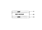
図5に、従来のインダクタ内蔵用基板の第2例を断面図で示す。絶縁性の樹脂単独層43の両面に金属層41が形成されている。この構成のインダクタ内蔵用基板は、曲げに強く、折れや割れが発生しにくいが、樹脂の比透磁率が1程度しかないため、大きなインダクタンスを得ることが難しいという問題を有する。
【0013】
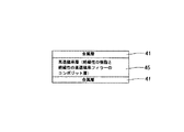
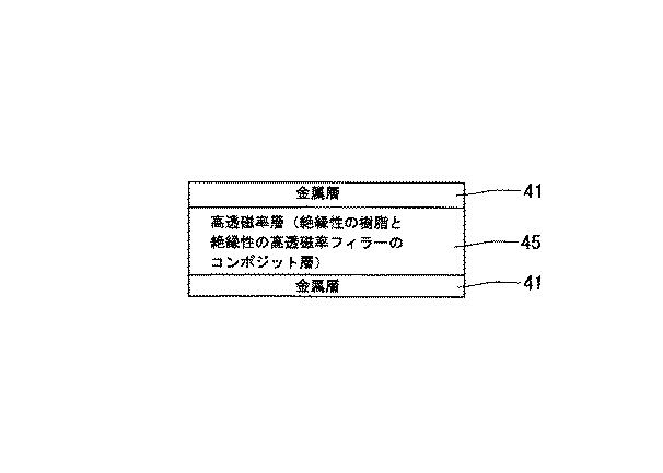
図6に、従来のインダクタ内蔵用基板の第3例を断面図で示す。絶縁性の樹脂と絶縁性の高透磁率フィラーとのコンポジット層である高透磁率層45の両面に金属層41が形成されている。この構成のインダクタ内蔵用基板は、比較的に曲げに強く、折れや割れが発生しにくいが、コンポジット層の比透磁率がせいぜい10〜15程度しか出せないため、大きなインダクタンスを得ることが難しいという問題を有する。
【0014】
【発明が解決しようとする課題】
既に説明したように、フェライト層を高透磁率のセラミック薄膜として使用した配線基板の場合、柔軟性が無いため、曲げに弱く、折れや割れが発生し易いという問題を有する。また、コアとなる層が絶縁性樹脂単独層の場合には、小さなインダクタンスしか得られない。更に、高透磁率層が絶縁性の樹脂と絶縁性の高透磁率フィラーからなるコンポジット層の場合においてもコンポジット層の比透磁率が10〜15程度となり、十分に大きなインダクタンスは得られない。
【0015】
この状況にあって、本発明の課題は、樹脂系の高透磁率粉末コンポジットタイプの、インダクタ内蔵用基板またはインダクタを内蔵した基板において、絶縁性を十分に保ったまま、従来の限界であった比透磁率が10〜15程度に対し、100程度の比透磁率を有する基板を提供することであり、またセラミック薄膜では不可能な柔軟性を有することにより、曲げに強く、折れや割れの発生しにくい基板を提供することである。
【0016】
【課題を解決するための手段】
本発明の第1の基板は、高透磁率層の両面に金属層が積層されたインダクタ内蔵用の基板であって、前記高透磁率層は、積層方向に垂直な断面内で交互に位置する2種類の部分層からなり、第1の部分層は、樹脂層、または樹脂と絶縁性の高透磁率フィラーとのコンポジット層であり、第2の部分層は、樹脂と導電性の高透磁率フィラーとのコンポジット層であることを特徴とする。
【0017】
本発明の第2の基板は、高透磁率層の両面に絶縁層を介して金属層が積層されたインダクタ内蔵用の基板であって、前記絶縁層は、樹脂層、または樹脂と絶縁性の高透磁率フィラーとからなるコンポジット層であり、前記高透磁率層は、積層方向に垂直な断面内で交互に位置する2種類の部分層からなり、第1の部分層は、樹脂層、または樹脂と絶縁性の高透磁率フィラーとのコンポジット層であり、第2の部分層は、樹脂と導電性の高透磁率フィラーとのコンポジット層であることを特徴とする。
【0018】
前記第1または第2の基板において、前記金属層は、白金、金、銀、銅、アルミニウム、ニッケル、コバルト、チタンのうちの少なくとも1つを含む金属、または前記金属による導電性ペーストを用いて形成することができる。
【0019】
本発明の第3の基板は、前記第1または第2の基板における前記金属層としてインダクタ用の金属パターンが設けられ、前記第1の部分層には導通ビアホールが設けられたことを特徴とする。
【0020】
【発明の実施の形態】
次に、本発明の実施の形態を説明する。
【0021】
本発明の実施の形態における第1のインダクタ内蔵用基板は、高透磁率層の両面に金属層が積層されたインダクタ内蔵用基板であって、前記高透磁率層は、積層方向に垂直な断面内で交互に位置する2種類の部分層からなり、第1の部分層は、樹脂層、または樹脂と絶縁性の高透磁率フィラーとのコンポジット層であり、第2の部分層は、樹脂と導電性の高透磁率フィラーとのコンポジット層とする。
【0022】
両面の金属層部分を互いに結ぶビアホールは、樹脂層、または樹脂と絶縁性の高透磁率フィラーとのコンポジット層である絶縁性の第1の部分層に形成する。
【0023】
また、ビアホールは、レーザーやエッチング等の確立された方法によって形成することができる。このビアホールは、めっきや導電性接着剤等の導電性物質によって各金属層同士の導通をとることに利用される。この構成により、絶縁性の第1の部分層のゆえに、第2の部分層における高透磁率フィラーが導電性の物質であるにもかかわらず、金属層同士を結ぶ導通ビアホールの周辺では絶縁性が保たれる。
【0024】
また、本発明の実施の形態における第2のインダクタ内蔵用基板は、第1のインダクタ内蔵用基板における高透磁率層と金属層とが直接接触しないように、その間に絶縁層が設けられた構成を有し、この絶縁層は、樹脂、または樹脂と絶縁性の高透磁率フィラーのコンポジット層とする。
【0025】
これは、第1のインダクタ内蔵用基板において、導通ビアホール周辺の絶縁が必要であるのと同様に、高透磁率層が樹脂と導電性の高透磁率フィラーとのコンポジットタイプであった場合、各金属層に挟まれている高透磁率層は、絶縁されている必要がある。絶縁層がない場合、使用条件によっては、各金属層と直に接触する高透磁率層に電流が流れてしまい、インダクタ形成時に、内蔵素子がインダクタとして働かなくなる場合があるからである。
【0026】
これを避けるため、第2のインダクタ内蔵用基板においては、金属層と導電性の高透磁率層の間に絶縁層として、樹脂層、または樹脂に絶縁性の高透磁率フィラーを混入したコンポジット層を挿入するものである。
【0027】
前記インダクタ内蔵用基板の各層に使用される樹脂としては、熱硬化性樹脂またはガラス転移温度(Tg)が80℃以上の熱可塑性樹脂を使用することが好ましい。
【0028】
熱硬化性樹脂としては、エポキシ樹脂、BT(ビスマレイミド・トリアジン)、ポリイミド樹脂、ポリアミドイミド樹脂、フェノール樹脂等が1種または2種以上組み合わせて使用される。
【0029】
また、熱可塑性樹脂としては飽和ポリエステル樹脂、アクリル樹脂等が1種または2種以上組み合わせて使用される。更に熱硬化性樹脂と熱可塑性樹脂を組み合わせて使用しても構わない。各部の樹脂は、同一のものを使用することが好ましいが、製造条件等により、異なった樹脂を使用しても構わない。このとき、樹脂同士の接着性や、たわみの違いによる反りの発生等には十分注意を要する。
【0030】
本実施の形態で使用される導電性の高透磁率粉末としては、鉄粉、センダスト粉、パーマロイ粉等が使用できる。形状は球形、鱗片状など制限はない。但し、透磁率をより高くするためには、アニール処理等を行い、歪みを除去した粉末を使用することが望ましい。
【0031】
本実施の形態で使用される絶縁性の高透磁率体粉末としては、Ni−Zn系フェライト、Mn−Zn系フェライト、コバルトフェライト、Cu−Zn−Mg系フェライト等がある。形状は球形、鱗片状など制限はない。但し、透磁率をより高くするためには、アニール処理等を行い、歪みを除去した粉末を使用することが望ましい。
【0032】
また、本実施の形態で使用される金属層は、白金、金、銀、銅、アルミニウム、ニッケル、コバルト、チタン及びこれらを含む合金で形成されているか、これらの金属粉末を用いた導電性ペーストで形成される。
【0033】
金属層は、めっき法や蒸着法で析出させても、始めから金属箔を使用して形成しても良い。導電性ペーストを使用する場合は、樹脂を含んでいても、いなくても問題はない。但し、樹脂を含まないものを使用する場合は、高温焼成用が多いため、使用する樹脂に影響が出ないような低温硬化品を選択する必要がある。
【0034】
本実施の形態のインダクタ内蔵用基板の金属層をエッチング等によりパターン化するか、導電性ペーストをパターン状に印刷すること等によりインダクタを内蔵した基板を得ることができる。当然、金属層の外表面に更に従来の多層基板製造技術による多層配線層を形成して、多層配線基板として使用することもできる。
【0035】
この様にして、樹脂系の高透磁率粉末コンポジットタイプの、インダクタ内蔵用基板またはインダクタを内蔵した基板において、絶縁性を十分に保ったまま、従来の限界であった比透磁率が10〜15程度に対し、100程度の比透磁率を有する基板を提供するものであり、更にセラミック薄膜では不可能な柔軟性を有することにより、曲げに強く、折れや割れの発生しにくい基板を提供することができる。
【0036】
【実施例】
以下、本発明の実施例を図面に基づいて説明する。
【0037】
(実施例1)図2は、実施例1のインダクタ内蔵基板のインダクタ部分を示す斜視図である。また、図3は、本実施例1のインダクタ内蔵基板のインダクタ部分を示す断面図である。21は高透磁率層、22は金属層のパターニング部分、23はビアホールを導体で埋めた部分を示す。
【0038】
金属層のエッチングや導電性接着剤の印刷等でストライプ状または格子状にパターニングして、上下の金属層間の導通格子部分を、めっきや導電性接着剤によりビアホール導通として、螺旋状パターンを作製し、インダクタとして作用させる。
【0039】
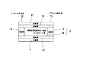
(実施例2)図1は、実施例2のインダクタ内蔵用基板を示す断面図である。11は金属層、12は絶縁層、13は第1の部分層、14は第2の部分層、15はビアホール形成部、16は高透磁率層を示す。
【0040】
図1に示すように、ビアホールは左右両側の絶縁性層である第1の部分層13に作製し、上下の金属層11をパターニングし、ビアホールで導通を取れば、第2の部分層14である導電性の高透磁率体コンポジット層をコアとするインダクタが形成できる。
【0041】
また、左右の絶縁性層(第1の部分層13)と高透磁率体コンポジット層(第2の部分層14)は互い違いに繰り返しパターンに配置された構成とすることができる。そうすれば、インダクタ内蔵用基板内に、必要に応じ、複数個のインダクタを、断面積や巻数を定めて必要なインダクタンスに設定して、内蔵することができる。
【0042】
このように、インダクタのコアとなる導電性の高透磁率のコンポジット層と、インダクタの導体となる金属層及びビアホール内の導体との間には絶縁性の層を設ける構造とした。
【0043】
次に、使用する原料、資材に関して説明する。
【0044】
金属層:片面電解銅箔(厚さ18μm)を使用した。
【0045】
樹脂:ビスフェノールA型エポキシ樹脂使用と柔軟性のあるビスフェノールA型フェノキシ樹脂を重量比で1:1に混合したもの(絶縁層、コンポジット層ともに使用した)。
【0046】
硬化剤:フェノールノボラック型硬化剤(絶縁層、コンポジット層ともに使用した)。
【0047】
溶剤:MEK(メチルエチルケトン)を使用した。
【0048】
導電性高透磁率粉末:鱗片状センダスト粉末(400#アンダー品)を使用した。
【0049】
なお、本実施例2では、絶縁層、並びにビアホールが設けられる絶縁性の部分層としては、樹脂を単独で使用した。
【0050】
引き続き、インダクタ内蔵用基板の製造方法について説明する。
【0051】
▲1▼:エポキシ樹脂と硬化剤及びフェノキシ樹脂を規定量混合し、MEKにて粘度調整後、スピンコーターにて銅箔の電解側に溶剤除去後10μm厚になるように調整し、塗布する。(絶縁層塗布の工程)
【0052】
▲2▼:120℃で30分程度、加熱乾燥し、MEKを除去し、樹脂層を半硬化状態にする。
【0053】
▲3▼:▲2▼の基板上に、導電性の高透磁率層として、センダスト粉末と樹脂を重量比で8:2の割合で混合したスラリーを幅10mmで、絶縁性の部分層として樹脂単独層を幅1mmで、格子状(ストライプ状)に、いずれも50μm厚で印刷し、再び▲2▼の工程を行う。
【0054】
▲4▼:▲3▼の層上に▲1▼→▲2▼の工程を再び行い、半硬化状態の樹脂層を10μm厚で形成する。
【0055】
▲5▼:▲4▼での半硬化状態の樹脂層上に、銅箔の電解側を樹脂層と接するように配置し真空ラミネートにより積層する。
【0056】
▲6▼:200℃で1時間プレス加熱硬化を行い、本実施例2のインダクタ内蔵用基板を得た。
【0057】
また、比較例1として、高透磁率層に、比透磁率2000のNi-Znフェライト薄膜のセラミック薄膜を用い、その両面に実施例2と同様の方法で金属層を設けて、インダクタ内蔵用基板を作製した。
【0058】
更に、比較例2として、高透磁率層に、絶縁性樹脂と、絶縁性の比透磁率2000のNi-Znフェライト粉とを重量比で2:8に混合したコンポジット層を用い、その両面に実施例2と同様の方法で金属層を設けてインダクタ内蔵用基板を作製した。
【0059】
次に、実施例2、比較例1、及び比較例2のインダクタ内蔵用基板の比透磁率と曲げ強度(柔軟性)を評価した結果を表1に示す。ビアホールは、1mm幅の絶縁性の部分層の中心に0.5mm径で作製し、導電性接着剤で上下の金属層と導通を取った。
【0060】
【表1】
【0061】
表1に示すように、本実施例のインダクタ内蔵用基板においては、絶縁性樹脂と絶縁性のNi-Znフェライト粉からなるコンポジット層を用いた比較例2と比べて、9倍の透磁率が得られると共に、セラミック薄膜を用いた比較例1と比べて、曲げ強度特性(柔軟性)が向上した。
【0062】
ところで、上記の実施例においては、導電性の高透磁率層と金属層の間の絶縁層、並びにビアホールが形成される絶縁性の部分層として、絶縁性の樹脂を単独で用いたが、これに換えて、樹脂に絶縁性の高透磁率体を混合してなる絶縁性のコンポジット層を用いると、更に高透磁率のインダクタ内蔵用基板が得られる。
【0063】
また、上記の実施例においては、導電性の高透磁率層と金属層の間に樹脂による絶縁層を用いたが、インダクタ内蔵基板の使用条件によっては、省略することもできる。
【0064】
【発明の効果】
上記のように、本発明の基板を使用することにより、従来の、高透磁率体がセラミックであるものより、耐折り曲げ性に優れ、柔軟性が高く、高透磁率体が樹脂と絶縁性の高透磁率体粉末とのコンポジット品である従来品に比べ透磁率を格段に大きくすることが可能となった。
【0065】
また、本発明の基板を使用することにより、絶縁性の高透磁率体粉末コンポジットタイプの10倍程度まで透磁率の調整が可能と考えられ、従来に比べインダクタンスの選択幅の広い基板の提供が可能となった。
【図面の簡単な説明】
【図1】本発明のインダクタ内蔵用基板の断面図。
【図2】本発明のインダクタ内蔵基板のインダクタ部分を示す斜視図。
【図3】本発明のインダクタ内蔵基板のインダクタ部分を示す断面図。
【図4】従来の第1のインダクタ内蔵用基板の断面図。
【図5】従来の第2のインダクタ内蔵用基板の断面図。
【図6】従来の第3のインダクタ内蔵用基板の断面図。
【符号の説明】
11 金属層
12 絶縁層
13 第1の部分層
14 第2の部分層
15 ビアホール形成部
16,21 高透磁率層
22 金属層のパターニング部分
23 ビアホールを導体で埋めた部分[0001]
TECHNICAL FIELD OF THE INVENTION
The present invention relates to a substrate having a built-in inductor, and more particularly, to a substrate suitable for use as a wiring substrate which has been enhanced in function with an increase in signal speed or wiring density.
[0002]
[Prior art]
Chip inductors are widely used as inductors for electric circuits. However, chip inductors require a lot of man-hours at the time of mounting, such as soldering, and can only be surface-mounted on a multilayer substrate, which has problems with high-density mounting and noise reduction.
[0003]
In other words, in recent years, demands for higher performance and smaller size of electronic devices have been accelerating, and the problem of noise generation due to higher speed and larger capacity of signals has been overlapped. It is necessary to improve noise and reduce noise by shortening the wiring distance. For this reason, in a wiring board, particularly a multilayer substrate, an inductor is formed by patterning a conductor in the substrate as much as possible.
[0004]
By the way, in the case of forming an inductor by patterning a conductor in a substrate, when the core material of the inductor is a resin, the relative permeability is only as small as about 1.
[0005]
To improve this, attempts have been made to mix a high magnetic permeability filler in a resin as a core material. However, when an insulating Ni—Zn-based ferrite or Mn—Zn-based ferrite is used as the high magnetic permeability filler, even if a ceramic thin film having a relative magnetic permeability of about 2000 is used, the composite with the resin can be used. As a film, the limit is to obtain a relative magnetic permeability of about 10 to 15.
[0006]
In addition, when a conductive high magnetic permeability filler is used, for example, as a simple substance, iron, cobalt, or nickel, and as an alloy, sendust, permalloy, or the like, it is possible to obtain a relative magnetic permeability of about 100 even in a resin composite system. It is possible. However, in this resin composite system, as a result of using a conductive high permeability filler, the composite film also has considerable conductivity, and current flows from the electrode of the circuit pattern into the composite film, The function as an inductor cannot be exhibited due to a short circuit or the like. Therefore, it cannot be used as an inductor layer in the substrate.
[0007]
By the way, when an insulating Ni—Zn-based ferrite or Mn—Zn-based ferrite is used as a ceramic thin film for the core material of the inductor, it is possible to obtain a relative magnetic permeability of several tens to several thousands.
[0008]
For example, there is a technique disclosed in the following Patent Document 1 as an example of a ceramic wiring board in which a ferrite layer is incorporated in a board and an inductor is built.
[0009]
[Patent Document 1]
JP-A-6-21264
Here, the prior art will be generally classified into three types.
[0011]
FIG. 4 is a cross-sectional view showing a first example of a conventional substrate with a built-in inductor. 41 is a metal layer, 42 is a high magnetic permeability layer of an insulating ceramic thin film. The substrate with a built-in inductor of this configuration can obtain a large inductance, but has a problem that it is weak in bending and easily breaks or cracks. Note that the ceramic wiring board of Patent Document 1 can be said to be an example in which an inductor conductor is formed in a layer corresponding to the metal layer 41 shown in FIG.
[0012]
FIG. 5 is a cross-sectional view showing a second example of a conventional substrate with a built-in inductor. The metal layers 41 are formed on both surfaces of the insulating resin single layer 43. The substrate with a built-in inductor having this configuration is resistant to bending and is unlikely to be broken or cracked, but has a problem that it is difficult to obtain a large inductance because the resin has a relative magnetic permeability of only about 1.
[0013]
FIG. 6 is a cross-sectional view showing a third example of a conventional substrate with a built-in inductor. Metal layers 41 are formed on both surfaces of a high magnetic permeability layer 45 which is a composite layer of an insulating resin and an insulating high magnetic permeability filler. The substrate with a built-in inductor of this configuration is relatively resistant to bending and is unlikely to break or crack, but it is difficult to obtain a large inductance because the relative permeability of the composite layer is only about 10 to 15 at most. Have a problem.
[0014]
[Problems to be solved by the invention]
As described above, a wiring board using a ferrite layer as a ceramic thin film having a high magnetic permeability has a problem in that it has no flexibility, is weak in bending, and easily breaks or cracks. When the core layer is a single layer of the insulating resin, only a small inductance can be obtained. Further, even when the high magnetic permeability layer is a composite layer composed of an insulating resin and an insulating high magnetic permeability filler, the relative magnetic permeability of the composite layer is about 10 to 15, and a sufficiently large inductance cannot be obtained.
[0015]
In this situation, an object of the present invention is a conventional limit of a resin-based high-magnetic-permeability powder composite type, in a substrate with a built-in inductor or a substrate with a built-in inductor, while maintaining sufficient insulation. It is an object of the present invention to provide a substrate having a relative magnetic permeability of about 100 with respect to a relative magnetic permeability of about 10 to 15, and having flexibility not possible with a ceramic thin film, thereby being strong against bending and causing breakage and cracking. It is to provide a substrate that is difficult to perform.
[0016]
[Means for Solving the Problems]
A first substrate according to the present invention is a substrate for incorporating an inductor in which a metal layer is laminated on both surfaces of a high magnetic permeability layer, wherein the high magnetic permeability layers are alternately located in a cross section perpendicular to the laminating direction. The first partial layer is a resin layer or a composite layer of a resin and an insulating high magnetic permeability filler, and the second partial layer is a resin and a conductive high magnetic permeability. It is a composite layer with a filler.
[0017]
The second substrate of the present invention is a substrate for incorporating an inductor, in which a metal layer is laminated on both surfaces of a high magnetic permeability layer via an insulating layer, wherein the insulating layer is a resin layer or a resin having an insulating property. A high permeability filler, wherein the high permeability layer is composed of two types of partial layers alternately positioned in a cross section perpendicular to the lamination direction, and the first partial layer is a resin layer or It is a composite layer of a resin and an insulating high magnetic permeability filler, and the second partial layer is a composite layer of a resin and a conductive high magnetic permeability filler.
[0018]
In the first or second substrate, the metal layer is formed using a metal including at least one of platinum, gold, silver, copper, aluminum, nickel, cobalt, and titanium, or a conductive paste including the metal. Can be formed.
[0019]
A third substrate according to the present invention is characterized in that a metal pattern for an inductor is provided as the metal layer in the first or second substrate, and a conductive via hole is provided in the first partial layer. .
[0020]
BEST MODE FOR CARRYING OUT THE INVENTION
Next, an embodiment of the present invention will be described.
[0021]
The first substrate with a built-in inductor according to an embodiment of the present invention is a substrate with a built-in inductor in which a metal layer is laminated on both surfaces of a high magnetic permeability layer, wherein the high magnetic permeability layer has a cross section perpendicular to the laminating direction. The first partial layer is a resin layer or a composite layer of a resin and an insulating high magnetic permeability filler, and the second partial layer is a resin layer or a resin layer. It is a composite layer with a conductive high magnetic permeability filler.
[0022]
The via hole connecting the metal layer portions on both surfaces is formed in a resin layer or an insulating first partial layer which is a composite layer of a resin and an insulating high magnetic permeability filler.
[0023]
In addition, the via hole can be formed by an established method such as laser or etching. The via holes are used to establish conduction between the metal layers by a conductive substance such as plating or a conductive adhesive. With this configuration, because of the insulating first partial layer, even though the high permeability filler in the second partial layer is a conductive substance, the insulating property around the conductive via hole connecting the metal layers is low. Will be kept.
[0024]
Further, the second substrate with a built-in inductor according to the embodiment of the present invention has a structure in which an insulating layer is provided between the high-permeability layer and the metal layer in the first substrate with a built-in inductor so as not to come into direct contact with each other. This insulating layer is a resin or a composite layer of a resin and a high magnetic permeability filler which is insulative with the resin.
[0025]
This is because when the high magnetic permeability layer is a composite type of a resin and a conductive high magnetic permeability filler, each The high magnetic permeability layer sandwiched between the metal layers needs to be insulated. If the insulating layer is not provided, current flows through the high magnetic permeability layer that is in direct contact with each metal layer depending on the use conditions, and the built-in element may not work as an inductor when the inductor is formed.
[0026]
To avoid this, in the second substrate with a built-in inductor, a resin layer or a composite layer obtained by mixing a resin with an insulating high magnetic permeability filler is used as an insulating layer between the metal layer and the conductive high magnetic permeability layer. Is inserted.
[0027]
It is preferable to use a thermosetting resin or a thermoplastic resin having a glass transition temperature (Tg) of 80 ° C. or more as a resin used for each layer of the substrate with a built-in inductor.
[0028]
As the thermosetting resin, an epoxy resin, BT (bismaleimide / triazine), a polyimide resin, a polyamideimide resin, a phenol resin, or the like is used alone or in combination of two or more.
[0029]
In addition, as the thermoplastic resin, a saturated polyester resin, an acrylic resin, or the like is used alone or in combination of two or more. Further, a thermosetting resin and a thermoplastic resin may be used in combination. It is preferable to use the same resin for each part, but different resins may be used depending on manufacturing conditions and the like. At this time, it is necessary to pay close attention to the adhesiveness between the resins and the occurrence of warpage due to the difference in bending.
[0030]
As the conductive high magnetic permeability powder used in the present embodiment, iron powder, sendust powder, permalloy powder and the like can be used. The shape is not limited, such as a sphere or a scale. However, in order to further increase the magnetic permeability, it is desirable to use a powder that has been subjected to an annealing treatment or the like and from which distortion has been removed.
[0031]
Examples of the insulating high magnetic permeability powder used in the present embodiment include Ni—Zn ferrite, Mn—Zn ferrite, cobalt ferrite, and Cu—Zn—Mg ferrite. The shape is not limited, such as a sphere or a scale. However, in order to further increase the magnetic permeability, it is desirable to use a powder that has been subjected to an annealing treatment or the like and from which distortion has been removed.
[0032]
Further, the metal layer used in the present embodiment is formed of platinum, gold, silver, copper, aluminum, nickel, cobalt, titanium and an alloy containing these, or a conductive paste using these metal powders. Is formed.
[0033]
The metal layer may be deposited by a plating method or a vapor deposition method, or may be formed using a metal foil from the beginning. When using a conductive paste, there is no problem whether or not the resin is contained. However, when a resin-free material is used, it is necessary to select a low-temperature-cured product that does not affect the resin to be used because it is often used for high-temperature baking.
[0034]
A substrate with a built-in inductor can be obtained by patterning the metal layer of the substrate with a built-in inductor of the present embodiment by etching or by printing a conductive paste in a pattern. Naturally, a multi-layer wiring layer formed by a conventional multi-layer substrate manufacturing technique can be further formed on the outer surface of the metal layer to be used as a multi-layer wiring substrate.
[0035]
In this manner, the resin-based high-permeability powder composite type substrate with a built-in inductor or a substrate with a built-in inductor has a relative permeability of the conventional limit of 10 to 15 while maintaining sufficient insulation. The present invention provides a substrate having a relative magnetic permeability of about 100, and further has a flexibility which is impossible with a ceramic thin film, thereby providing a substrate which is resistant to bending and is hardly broken or cracked. Can be.
[0036]
【Example】
Hereinafter, embodiments of the present invention will be described with reference to the drawings.
[0037]
(Embodiment 1) FIG. 2 is a perspective view showing an inductor portion of a substrate with a built-in inductor according to Embodiment 1. FIG. FIG. 3 is a cross-sectional view illustrating an inductor portion of the substrate with a built-in inductor according to the first embodiment. 21 indicates a high magnetic permeability layer, 22 indicates a patterned portion of a metal layer, and 23 indicates a portion in which a via hole is filled with a conductor.
[0038]
A spiral pattern is formed by patterning the conductive grid portion between the upper and lower metal layers with via holes by using plating or conductive adhesive by patterning it into stripes or grids by etching the metal layer or printing a conductive adhesive. , Acting as an inductor.
[0039]
(Embodiment 2) FIG. 1 is a sectional view showing a substrate with a built-in inductor according to a second embodiment. Reference numeral 11 denotes a metal layer, 12 denotes an insulating layer, 13 denotes a first partial layer, 14 denotes a second partial layer, 15 denotes a via hole forming portion, and 16 denotes a high magnetic permeability layer.
[0040]
As shown in FIG. 1, via holes are formed in the first partial layer 13 which is an insulating layer on both the left and right sides, and the upper and lower metal layers 11 are patterned. An inductor having a core of a certain conductive high permeability composite layer can be formed.
[0041]
The left and right insulating layers (the first partial layer 13) and the high-permeability composite layer (the second partial layer 14) may be alternately arranged in a repeated pattern. Then, if necessary, a plurality of inductors can be set in a required inductance by setting the cross-sectional area and the number of turns in the inductor built-in substrate, and can be embedded therein.
[0042]
As described above, the structure is such that the insulating layer is provided between the conductive high-permeability composite layer serving as the inductor core and the metal layer serving as the inductor conductor and the conductor in the via hole.
[0043]
Next, the raw materials and materials used will be described.
[0044]
Metal layer: Single-sided electrolytic copper foil (18 μm thick) was used.
[0045]
Resin: A mixture of a bisphenol A type epoxy resin and a flexible bisphenol A type phenoxy resin in a weight ratio of 1: 1 (both insulating and composite layers were used).
[0046]
Curing agent: Phenol novolak type curing agent (used for both insulating layer and composite layer).
[0047]
Solvent: MEK (methyl ethyl ketone) was used.
[0048]
Conductive high permeability powder: Scaly sendust powder (400 # under product) was used.
[0049]
In Example 2, resin was used alone as the insulating layer and the insulating partial layer in which the via hole was provided.
[0050]
Subsequently, a method of manufacturing the substrate with a built-in inductor will be described.
[0051]
{Circle around (1)}: A specified amount of an epoxy resin, a curing agent and a phenoxy resin are mixed, the viscosity is adjusted by MEK, the solvent is removed to the electrolytic side of the copper foil by a spin coater, and the thickness is adjusted to 10 μm and applied. (Process of applying insulating layer)
[0052]
{Circle around (2)}: Heat drying at 120 ° C. for about 30 minutes to remove MEK, and bring the resin layer into a semi-cured state.
[0053]
{Circle around (3)} On the substrate of {circle around (2)}, a slurry in which sendust powder and resin were mixed at a weight ratio of 8: 2 as a conductive high magnetic permeability layer with a width of 10 mm and a resin as an insulating partial layer was used. The single layer is printed with a width of 1 mm and a lattice shape (striped shape) with a thickness of 50 μm, and the step (2) is performed again.
[0054]
{Circle around (4)} The steps {circle around (1)} → {circle around (2)} are performed again on the layer {circle around (3)} to form a semi-cured resin layer with a thickness of 10 μm.
[0055]
(5): The copper foil is placed on the semi-cured resin layer in (4) such that the electrolytic side of the copper foil is in contact with the resin layer, and laminated by vacuum lamination.
[0056]
{Circle around (6)}: Press-curing was performed at 200 ° C. for 1 hour to obtain a substrate with a built-in inductor of Example 2.
[0057]
Further, as Comparative Example 1, a ceramic thin film of a Ni—Zn ferrite thin film having a relative magnetic permeability of 2000 was used for the high magnetic permeability layer, and a metal layer was provided on both surfaces thereof in the same manner as in Example 2. Was prepared.
[0058]
Further, as Comparative Example 2, a composite layer obtained by mixing an insulating resin and an insulating Ni—Zn ferrite powder having a relative magnetic permeability of 2,000 at a weight ratio of 2: 8 was used for the high magnetic permeability layer, and both surfaces thereof were used. A metal layer was provided in the same manner as in Example 2 to produce a substrate with a built-in inductor.
[0059]
Next, Table 1 shows the results of evaluating the relative magnetic permeability and the bending strength (flexibility) of the substrates with built-in inductors of Example 2, Comparative Example 1, and Comparative Example 2. The via hole was formed with a diameter of 0.5 mm at the center of the insulating partial layer having a width of 1 mm, and was electrically connected to the upper and lower metal layers with a conductive adhesive.
[0060]
[Table 1]
[0061]
As shown in Table 1, in the substrate with a built-in inductor of the present example, the magnetic permeability was 9 times higher than that of Comparative Example 2 using the composite layer made of insulating resin and insulating Ni—Zn ferrite powder. As well as being obtained, the bending strength characteristics (flexibility) were improved as compared with Comparative Example 1 using a ceramic thin film.
[0062]
By the way, in the above embodiment, the insulating resin is used alone as the insulating layer between the conductive high magnetic permeability layer and the metal layer, and as the insulating partial layer where the via hole is formed. Instead, when an insulating composite layer obtained by mixing an insulating material with a high magnetic permeability in a resin is used, a substrate with a higher magnetic permeability and a built-in inductor can be obtained.
[0063]
In the above embodiment, an insulating layer made of a resin is used between the conductive high magnetic permeability layer and the metal layer. However, the insulating layer may be omitted depending on the use conditions of the inductor built-in substrate.
[0064]
【The invention's effect】
As described above, by using the substrate of the present invention, the conventional high-permeability body is more excellent in bending resistance and flexibility than the ceramic having a high permeability, and the high-permeability body has resin and insulating properties. The magnetic permeability can be remarkably increased as compared with a conventional product which is a composite product with a high permeability powder.
[0065]
In addition, by using the substrate of the present invention, it is considered that the permeability can be adjusted up to about 10 times that of the insulating high-permeability powder composite type. It has become possible.
[Brief description of the drawings]
FIG. 1 is a cross-sectional view of a substrate for incorporating an inductor of the present invention.
FIG. 2 is a perspective view showing an inductor portion of the substrate with a built-in inductor of the present invention.
FIG. 3 is a sectional view showing an inductor portion of the substrate with a built-in inductor of the present invention.
FIG. 4 is a cross-sectional view of a first conventional substrate with a built-in inductor.
FIG. 5 is a cross-sectional view of a second conventional substrate with a built-in inductor.
FIG. 6 is a cross-sectional view of a third conventional substrate with a built-in inductor.
[Explanation of symbols]
DESCRIPTION OF SYMBOLS 11 Metal layer 12 Insulating layer 13 1st partial layer 14 2nd partial layer 15 Via hole formation part 16, 21 High permeability layer 22 Metal layer patterning part 23 The part which filled a via hole with a conductor