JP2004207385A - Mask, method of manufacturing the same, and method of manufacturing semiconductor device using the same - Google Patents
Mask, method of manufacturing the same, and method of manufacturing semiconductor device using the same Download PDFInfo
- Publication number
- JP2004207385A JP2004207385A JP2002372859A JP2002372859A JP2004207385A JP 2004207385 A JP2004207385 A JP 2004207385A JP 2002372859 A JP2002372859 A JP 2002372859A JP 2002372859 A JP2002372859 A JP 2002372859A JP 2004207385 A JP2004207385 A JP 2004207385A
- Authority
- JP
- Japan
- Prior art keywords
- mask
- junction
- substrate
- processed
- ion implantation
- Prior art date
- Legal status (The legal status is an assumption and is not a legal conclusion. Google has not performed a legal analysis and makes no representation as to the accuracy of the status listed.)
- Pending
Links
Images









Classifications
-
- G—PHYSICS
- G03—PHOTOGRAPHY; CINEMATOGRAPHY; ANALOGOUS TECHNIQUES USING WAVES OTHER THAN OPTICAL WAVES; ELECTROGRAPHY; HOLOGRAPHY
- G03F—PHOTOMECHANICAL PRODUCTION OF TEXTURED OR PATTERNED SURFACES, e.g. FOR PRINTING, FOR PROCESSING OF SEMICONDUCTOR DEVICES; MATERIALS THEREFOR; ORIGINALS THEREFOR; APPARATUS SPECIALLY ADAPTED THEREFOR
- G03F1/00—Originals for photomechanical production of textured or patterned surfaces, e.g., masks, photo-masks, reticles; Mask blanks or pellicles therefor; Containers specially adapted therefor; Preparation thereof
- G03F1/20—Masks or mask blanks for imaging by charged particle beam [CPB] radiation, e.g. by electron beam; Preparation thereof
-
- H—ELECTRICITY
- H10—SEMICONDUCTOR DEVICES; ELECTRIC SOLID-STATE DEVICES NOT OTHERWISE PROVIDED FOR
- H10P—GENERIC PROCESSES OR APPARATUS FOR THE MANUFACTURE OR TREATMENT OF DEVICES COVERED BY CLASS H10
- H10P76/00—Manufacture or treatment of masks on semiconductor bodies, e.g. by lithography or photolithography
-
- H—ELECTRICITY
- H01—ELECTRIC ELEMENTS
- H01J—ELECTRIC DISCHARGE TUBES OR DISCHARGE LAMPS
- H01J2237/00—Discharge tubes exposing object to beam, e.g. for analysis treatment, etching, imaging
- H01J2237/04—Means for controlling the discharge
- H01J2237/045—Diaphragms
- H01J2237/0451—Diaphragms with fixed aperture
- H01J2237/0453—Diaphragms with fixed aperture multiple apertures
-
- H—ELECTRICITY
- H01—ELECTRIC ELEMENTS
- H01J—ELECTRIC DISCHARGE TUBES OR DISCHARGE LAMPS
- H01J2237/00—Discharge tubes exposing object to beam, e.g. for analysis treatment, etching, imaging
- H01J2237/30—Electron or ion beam tubes for processing objects
- H01J2237/317—Processing objects on a microscale
- H01J2237/31701—Ion implantation
- H01J2237/31706—Ion implantation characterised by the area treated
- H01J2237/3171—Ion implantation characterised by the area treated patterned
- H01J2237/31711—Ion implantation characterised by the area treated patterned using mask
-
- H—ELECTRICITY
- H01—ELECTRIC ELEMENTS
- H01J—ELECTRIC DISCHARGE TUBES OR DISCHARGE LAMPS
- H01J2237/00—Discharge tubes exposing object to beam, e.g. for analysis treatment, etching, imaging
- H01J2237/30—Electron or ion beam tubes for processing objects
- H01J2237/317—Processing objects on a microscale
- H01J2237/3175—Lithography
- H01J2237/31793—Problems associated with lithography
- H01J2237/31794—Problems associated with lithography affecting masks
Landscapes
- Physics & Mathematics (AREA)
- General Physics & Mathematics (AREA)
- Electron Beam Exposure (AREA)
- Drying Of Semiconductors (AREA)
- Micromachines (AREA)
Abstract
【課題】反りや変形を生じることなく高精度で信頼性の高いマスクを提供することを目的とする。また、イオン注入技術において、高精度のイオン注入を行うことのできる(ステンシル)マスクを提供する。レジストパターンの形成を必要とすることなく、高精度で信頼性の高いイオン注入方法を提供する。
【解決手段】マスクパターン部と、少なくともひとつのpn接合部とを備えた板状体と、前記pn接合部に電流供給を行う電流供給部とを具備し、前記pn接合部に通電することにより、ペルチェ効果を生起し、前記マスクパターン部の温度を制御できるマスクを提供する。またこのマスクを用いてレジストパターンを形成することなく、信頼性の高いイオン注入領域の形成が可能となる。
【選択図】図3An object of the present invention is to provide a highly accurate and highly reliable mask without warping or deformation. Further, in the ion implantation technique, a (stencil) mask capable of performing highly accurate ion implantation is provided. Provided is a highly accurate and highly reliable ion implantation method without requiring formation of a resist pattern.
A plate-like body having a mask pattern portion and at least one pn junction portion, and a current supply portion for supplying a current to the pn junction portion, wherein a current is supplied to the pn junction portion The present invention provides a mask that generates a Peltier effect and can control the temperature of the mask pattern portion. Further, a highly reliable ion implantation region can be formed without forming a resist pattern using this mask.
[Selection diagram] FIG.
Description
【0001】
【発明の属する技術分野】
本発明は、マスク、その製造方法、これを用いた半導体装置の製造方法および半導体製造装置に係り、特に、処理工程中におけるマスクの温度上昇による歪の低減に関する。
【0002】
【従来の技術】
近年半導体装置の微細化、高集積化は進む一方であり、サブクオータミクロンの加工を高精度かつ再現性よく行う技術が必要となってきている。
【0003】
例えば、半導体集積回路(LSI)を形成する場合、ウェルの形成、チャネル部の形成、ソース・ドレイン領域の形成、コンタクト領域の形成などLSIの形成工程においては、数回から10回のイオン注入工程を必要とする。通常は基板表面にレジストを塗布し、選択露光を行い、現像工程を経て、フォトリソグラフィによりレジストパターンを形成し、このレジストパターンを介してイオン注入を行うことにより、レジストパターンの開口領域にイオン注入がなされる。
【0004】
例えば図18(a)乃至(e)に、このイオン注入工程の一例を示す。図18(a)に示すように、シリコン基板11表面にLOCOS法により素子分離絶縁膜12を形成し、素子領域を分離した後、基板表面全体にレジストRを塗布する。
【0005】
この後、図18(b)に示すように、フォトマスクを介して露光を行い、感光領域を形成し、図18(c)に示すように、感光領域のレジストを現像により除去し、レジストパターンRを形成する。
【0006】
そして、図18(d)に示すように、レジストパターンRを介してイオン注入を行い、イオン注入領域13を形成する。
【0007】
最後に、レジストパターンRを除去し、熱拡散を行い図18(e)に示すように、所望の深さのイオン注入領域13(拡散領域)を形成する。
【0008】
このように、レジスト塗布、露光・現像によるパターニング、そしてイオン注入後に剥離する必要がある場合が多く、多くの工程を必要とする上、ウェット工程を経るため、基板表面の汚染も大きな問題となっている。
また、このようなリソグラフィ工程を経てパターン形成を行う場合、露光用マスクに一旦焼き付けたパターンを介して露光を行うため、転写による精度低下も問題となっている。
【0009】
ところで、半導体製造技術のうちの一つである荷電粒子・電子線等の露光装置用にステンシルマスクが提案されている。
電子線等を走査し、ウェーハ(半導体基板)に微細パターンを直接描きこむ直描技術は処理時間が非常に長いため、電子線等をパターン通りに走査することをやめ、開口パターンを有するマスク(ステンシルマスク)を用い、ウェーハ(半導体基板)に電子線等が選択的に照射される構成にすることで処理時間の短縮化を狙っている。
【0010】
このマスク技術をイオン注入技術に応用すると、イオン注入時にレジストマスクを用いずにステンシルマスクを用いることでイオンビームをウェーハ(基板)内に選択的に導入することができる。これによりレジスト塗布・露光・現像によるパターニングと、イオン注入後のレジスト剥離などの工程が削減できると同時にWET工程を経ることが無いためウェーハ表面汚染が無く、短時間でのパターン形成処理が可能となる。
【0011】
しかしながらこの場合、イオンがマスクに直接照射されるため、マスク温度が大きく上昇し、マスク構成材が大きく膨張し反りやゆがみ等を発生させ、パターン精度が低下してしまう。という問題がある。
【0012】
図20(a)および(b)に、常温時と高温時とのステンシルマスクMの変位を模式的に示す。高温時では変位d(マスクのたわみ)が大きくなっており、パターンの開口位置・開口精度のずれは極めて大きなものとなることがわかる。
【0013】
例えば図19に示すように30mm2厚さ10umのメンブレン部の中央に熱電対Kを配置したステンシルマスクMを介してウェーハ(半導体基板)表面にイオン注入を行いステンシルマスクの温度上昇およびメンブレン部の変位(たわみ)を測定した結果を図21、22に示す。
このときのイオン注入条件はボロンをエネルギー90keV、ドーズ量2E13ions/cm2とし、ビームパワーを変化させて注入を実施した。
【0014】
図21、22からあきらかなように、ビームの注入によってステンシルマスクの温度が大きく上昇し、変位が発生していることがわかる。
このように従来の技術では、ステンシルマスクでは、高精度のパターン形成を行うことができないという問題があった。
【0015】
この問題は、イオン注入、イオンビームエッチングなどイオンの関与する技術のみならず、荷電粒子・電子線等の露光工程やエッチング工程や成膜工程においても同様であり、パターンの微細化に伴い、わずかな温度変化も大きな問題となることがわかる。
【0016】
本発明は前記実情に鑑みてなされたもので、反りや変形を生じることなく高精度で信頼性の高いマスクを提供することを目的とする。
【0017】
また本発明では、イオン注入技術において、高精度のイオン注入を行うことのできる(ステンシル)マスクを提供することを目的とする。
【0018】
また、高精度パターンを形成することのできる半導体処理工程用マスクを提供することを目的とする。
【0019】
さらに、製造が容易で信頼性の高いマスクの製造方法を提供することを目的とする。
【0020】
また、レジストパターンの形成を必要とすることなく、高精度で信頼性の高いイオン注入方法およびイオン注入装置を提供することを目的とする。
【0021】
また、レジストパターンの形成を必要とすることなく、高精度で信頼性の高いエッチング方法あるいは成膜方法を提供することを目的とする。
【0022】
【課題を解決するための手段】
そこで本発明のマスクは、マスクパターン部と、pn接合部とを備えた板状体と、前記pn接合部に電流供給を行う電流供給部とを具備し、前記pn接合部に通電することにより、ペルチェ効果を生起し、前記マスクパターン部の温度を制御できるようにしたことを特徴とする。
【0023】
本発明は、pn接合部に電流を流しペルチェ効果を生起せしめることにより、マスク自体の温度を制御するようにしたものである。すなわち、pn接合部に対し、n型領域からp型領域に向かう方向に電流を流すと、電子は、接合面(側の電極)からn型領域に移動し、n型領域を通過するためのエネルギーを、接合面側の電極から吸収して通過しようとし、n型領域の他端側の電極(通電電極)にこのエネルギーを放出して通過する。一方正孔は、接合面(側の電極)からp型領域に移動し、p型領域を通過するためのエネルギーを、接合面側の電極から吸収して通過しようとし、p型領域の他端側の電極(通電電極)にこのエネルギーを放出して通過する。その結果、接合面側でエネルギーが不足し、温度が下がる。従って、pn接合に与える電流の方向あるいは電流量を制御することにより、熱の輸送を調整し、マスクの温度を所望の温度に調整することが可能となる。これは電気的な制御によって容易に制御可能であるため、高精度の温度調整が可能となり、マスク上のパターンのずれを防ぎ、高精度のパターン形成を実現することが可能となる。
【0024】
本発明によれば、特にイオン注入用のマスクなどのイオンの衝突による温度上昇の生じ易い用途に用いられるマスクについて、マスクパターン部がペルチェ効果により冷却可面となるように構成されていれば、反りや歪を防止し、信頼性の高いパターン形成を行うことが可能となり、特に有効である。
【0025】
特にこの板状体は、マスクパターン部を有する膜厚の薄いメンブレン部と、前記メンブレン部の周縁に形成された枠状の支持部とを具備するようにすれば、取り扱いが容易である。またCMOSデバイスの形成の場合pウェルとnウェルを形成する必要があるが、2回のレジストパターンの形成工程が必要となる。すなわち、従来の方法では、一方の導電型の不純物イオンを注入するためのレジスト塗布・パターニング工程を経て、イオン注入を行ったのちレジストを除去する。そして、この後さらに導電型の不純物イオンを注入するためのレジスト塗布・パターニング工程を経て、イオン注入を行い、レジストを除去する。このため、ウェハを多数回のウェットプロセスを通過させる必要がある上、チャンバーからの出し入れに際しても汚染の原因が多数存在する。
【0026】
しかしながら本発明のマスクを用いるようにすれば、この支持部をつかんでイオン注入装置などの処理装置内で、マスクの着脱が自在である。従って、作業性よくマスクを取り替えて順次複数回のイオン注入が可能となり、大幅な作業性の向上をはかることが可能となる。
【0027】
また望ましくは、メンブレン部と支持部とは、一枚の半導体基板で構成すれば、熱伝導により温度制御が容易となり、熱による歪の発生も抑制できる。
【0028】
また、前記メンブレン部は、シリコン基板で構成すれば、通常の半導体プロセスで容易に精度よくpn接合を形成することが可能となる。また、半導体プロセスでマスクとして使用する際にも、被処理物と同じ元素であるためイオン注入装置などの処理装置内の汚染原因とならない。
【0029】
また、pn接合部は、前記板状体の表面に、互いに平行となるように形成されたストライプ状のp型不純物領域とn型不純物領域で構成し、pn接合部をメンブレン部の表面と垂直な面上に形成されているようにすれば、微細加工を施すことで、接合周囲長を長くすることができ、温度制御効率の高いマスクを提供することが可能となるという効果がある。
【0030】
また、pn接合部を、図11に示すように、前記板状体の表面に、比較的深く形成されたウェル領域の中に櫛歯状の比較的浅い拡散パターンで構成すれば、pn接合部の面積を最大限に大きくとることができ、効率よく温度制御を行うことが可能となる。
【0031】
また、pn接合部を板状体の表面から所定の深さ位置で表面に平行に形成した場合は、pn接合が表面に対し均一な密度で存在するため、面方向の温度分布を均一にすることが可能となると同時に、深部にpn接合が形成されるためメンブレン表面近傍のイオンビーム不純物の残留によるpn接合特性への影響を受けにくい、温度制御特性の安定した信頼性の高いマスクを提供することが可能となる。
【0032】
望ましくは、マスクを構成するシリコン基板上に、pn接合部からなる温度検出部を形成すれば、高精度に温度検出を行うことができ、効率よく高精度の温度制御を行うことが可能となる。
【0033】
また、温度検出部のpn接合部を、前記メンブレン部のpn接合部を構成する拡散層と同一工程で形成された不純物領域で構成すれば、より容易に高精度な温度検出を行うことができる。そして、効率よく温度制御を行うことができるため、反りや歪のない高精度のマスクを形成することが可能となる。
【0034】
望ましくは、温度検出部を、メンブレン部よりも肉厚が大きくなるように形成された支持部(梁や枠)表面に形成すれば、強度的に安定なマスクを提供することが可能となる。
【0035】
また、pn接合部は、マスクパターン部に形成されているようにすれば、処理工程中に実際に温度変化を生じ易い領域であるマスクパターン形成部の温度を高精度に検出できるため、より高精度の温度制御が可能となり、ずれや変形のないマスクを提供することが出来る。
【0036】
また、pn接合部は、前記メンブレン部の開口部を除く領域に形成され、前記枠状の支持部とほぼ同一厚さを有する部分支持部(梁)に形成されるようにすれば、支持部をかねて温度制御部が形成されていることになり、剛性と信頼性の高いマスクを構成することが可能となる。
【0037】
さらにこのpn接合部は、前記部分支持部(梁)内に、前記メンブレン部の深部に表面と平行な面に形成されているようにすれば、メンブレン表面近傍のイオンビーム不純物の残留によるpn接合特性への影響を受けにくい、より長寿命のマスクを提供することが可能となる。
【0038】
さらにまたpn接合部は、前記部分支持部(梁)内に、前記メンブレン部の表面と垂直な面上に形成されているようにすれば、微細加工を施すことで、接合周囲長を長くすることができ、冷却効率の高いマスクを提供することが可能となるという効果がある。
【0039】
また、前記メンブレン部は、シリコンカーバイド基板で構成すれば、比較的精度の高くない電流制御や温度制御でも変形の少ないマスクとすることができるため、より簡単な構成の信頼性の高いマスクとすることができる。
【0040】
さらにまた、前記メンブレン部は、ダイヤモンド基板で構成すれば、硬くスパッタされにくく、安定であるため、汚染原因となりにくいという特徴がある。また、熱伝導性が良好である上、電気的には絶縁性を維持することができるため、マスク設計に自由度が大きい。
【0041】
また本発明のマスクの製造方法では、半導体基板表面に不純物イオンを注入し、少なくともひとつのpn接合部を形成する工程と、前記半導体基板表面にパターン部を形成する工程と、前記pn接合部に通電することにより、ペルチェ効果を生起しうるように電流供給を行う電流供給部を形成する工程とを含むことを特徴とする。なおこのマスクのパターン部は開口部の集合体で構成されるが、使用条件によっては、光あるいはイオンの透過領域と非透過領域とで構成されていればよく、必ずしも孔でなくてもよい。
【0042】
かかる方法によれば、通常の薄膜プロセスで容易にマスクを形成することが可能となる。
【0043】
また本発明の半導体装置の製造方法では、上記マスクを、被処理基板表面に位置合わせして装着する工程と、前記マスクを介して前記被処理基板に対して、物理的または化学的処理を選択的に施す処理工程とを含むことを特徴とする。
【0044】
かかる方法によれば、フォトリソグラフィ工程を経ることなくペルチェ効果を利用したマスクを用いてマスク表面の温度制御を行いながら、所望のパターンを高精度に形成することができる。ここで、処理は成膜、エッチング、改質(感光あるいは注入など)の処理を示し、物理的処理には、露光などの光学的処理、スパッタリングなど、化学的処理にはCVDなどの成膜処理あるいはRIEなどのエッチング処理などがある。
【0045】
またこの処理工程では、このマスクの開口部に相当する領域の前記被処理基板表面に選択的にイオン注入を行うようにすれば、ペルチェ効果を利用してマスク温度の上昇を防ぎ反りも歪もない状態でイオン注入を行うことが可能となる。
【0046】
さらにまた、この処理工程が、所望の開口部パターンの形成された第1のマスクを前記被処理基板表面に装着し、前記第1のマスクの開口部に相当する領域の前記被処理基板表面に第1の不純物イオンを注入する工程と、第1のマスクに代えて第2のマスクを前記第1の不純物イオンの注入された被処理基板表面に装着し,前記第2のマスクの開口部に相当する領域の前記被処理基板表面に第2の不純物イオンを注入する工程とを含むようにすれば、CMOS工程におけるイオン注入が極めて簡略化され、高精度で信頼性の高い不純物領域を作業性よく形成することが可能となる。
【0047】
望ましくは、前記処理工程は、前記マスクの開口部に相当する領域の前記被処理基板表面形成されたレジストを選択的に露光する露光工程を含むことを特徴とする。すなわち、電子ビーム(EB)露光などの露光用マスクとして用いるもので、この構成では、常にマスクが一定温度に保持されるため熱による歪もないため、高精度のマスクパターンを維持することができる。従ってビーム走査によって描画していた露光工程が、マスクを介した全面露光によって達成できるため、極めて作業性が良く、短時間で露光可能である上、再現性および制御性の高いものとなる。
【0048】
望ましくは、この処理工程では、前記マスクの開口部に相当する領域の前記被処理基板表面を選択的にエッチングする工程を含むようにすれば、フォトリソグラフィ工程を経ることなくエッチングが可能となる。特に気相エッチングの場合には、ウェット工程が不要となるため、汚染を防止し信頼性の向上をはかることが可能となる。
【0049】
望ましくは、処理工程は、前記マスクの開口部に相当する領域の前記被処理基板表面に選択的に薄膜を形成する成膜工程を含むようにすれば、フォトリソグラフィ工程もパターンエッチング工程も不要であり、信頼性の高いパターン形成を行うことが可能となる。
【0050】
本発明の半導体製造装置によれば、上記マスクと、前記マスクを被処理基板表面に位置合わせして装着する位置合わせ手段と、前記マスクを介して前記被処理基板表面に不純物イオンを注入するイオン注入手段と、前記マスクの温度が一定となるように前記pn接合部への通電を制御する制御手段とを具備したことを特徴とする。
【0051】
かかる装置によれば、高精度で信頼性の高いイオン注入領域の形成が極めて作業性よく実現可能となる。
【0052】
なお、温度制御を行いつつ処理を行う場合、あらかじめ、どの程度の温度上昇を生じるかを測定しておくようにすれば、所望の温度差を生起し得る程度の電流供給を行えばよく、作業性よく温度制御を行い、一定温度での制御を実現することが可能となる。
【0053】
【発明の実施の形態】
次に本発明の実施形態について図面を参照しつつ詳細に説明する。
(第1の実施の形態)
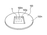
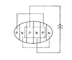
まず、図1および図2(図1は斜視図、図2は裏面からの斜視図である)に示すように、第1の実施の形態の不純物注入用マスク100は、SOI基板で構成されており、中央に孔hによってパターンを形成したマスクパターン部100pを具備したメンブレン部100mと,その周りに形成された枠状の支持部100nとを具備してなるものである。このメンブレン部がほぼ全面にわたり図3に概念図を示すようにpn接合部を有したペルチェ素子を構成しており、このpn接合部に電流供給を行うことにより、pn接合部に電流が流れて、ペルチェ効果を生起し、このメンブレン部の温度を制御できるようにしたことを特徴とする。このpn接合部への電流供給は図2にマスクの裏面側からみた斜視図を示すようにマスク裏面に形成されたパッド101を介してなされる。なおこの枠状の支持部100nの外側あるいは上側に熱的に接触するように水冷機構を設けるようにして、高温側を放熱する。
【0054】
この不純物注入用マスクは、図4に要部断面図を示すように、シリコン基板1表面に酸化シリコン膜2を介して形成されたノンドープシリコン層3表面に、ストライプ状をなすように、n型不純物領域4とp型不純物領域5とを交互に形成し、基板表面から所定の深さまで基板表面に沿って平行なpn接合部を形成してなるものである。6P,6Nはアルミニウム層からなるコンタクトパターンである。またn型不純物領域4とp型不純物領域5とにまたがるように、n型不純物領域4とp型不純物領域5との両方にオーミック接触をとるための金属層からなるペルチェ用パターン6Cが形成されている。
なおこのペルチェ用パターン6Cは、なくてもpn接合をブレークダウンさせることができる電圧域で使用すればペルチェ動作可能である。pn接合は1E15程度で7V程度、1E16程度で1V程度でもブレークダウンするので、pn接合の降伏電圧によりペルチェ素子としての使用電圧域を決定すればよい。
【0055】
次にこの不純物注入用マスクの製造方法について図5(a)乃至(e)を参照しつつ説明する。
まず、直接接合法により、シリコン基板1表面に形成された酸化シリコン膜2を介してノンドープのシリコン基板を接合し、所望の厚さに研磨することにより、ノンドープシリコン層3を形成する(SOI基板の形成)。
【0056】
このSOI基板を出発材料とし、図5(a)に示すように、フォトリソグラフィ法を用いて第1のレジストパターンR1を形成し、この第1のレジストパターンR1をマスクとしてn型の不純物イオンを注入し、n型不純物領域4を形成する。
【0057】
続いて、図5(b)に示すように、このレジストパターンR1を剥離除去し、更にフォトリソグラフィ法を用いて第2のレジストパターンR2を形成し、この第2のレジストパターンR2をマスクとしてp型の不純物イオンを注入し、p型不純物領域5を形成する。
【0058】
そして、このレジストパターンR2を剥離除去し、1000℃、30秒程度ののRTA等の活性化を行ったのち、図5(c)に示すように、更にフォトリソグラフィ法を用いてマスクパターン形成用の第3のレジストパターンR3を形成する。
【0059】
この後、この第3のレジストパターンR3をマスクとし、酸化シリコン膜2をエッチングストッパとして、RIEによりエッチングを行い、ホールhを形成する。
【0060】
そしてこの第3のレジストパターンR3をエッチング除去し、スパッタリング法やCVD法によりアルミニウム等のメタル層6を形成する。このメタル層の膜厚は使用電流によって決定されるが、厚いほど放熱効果が良く配線の信頼性も高くなる。そして更に図5(d)に示すように、フォトリソグラフィ法を用いてメタル層6パターニング用の第4のレジストパターンR4を形成する。
【0061】
そして、RIEなどのエッチングにより、メタル層6をパターニングする。
最後に、裏面にレジストパターン(図示せず)を形成し、これをマスクとしてエッチングを行い、メンブレン(薄膜)部を形成する。このエッチング工程でも酸化シリコン膜2をエッチングストッパとして用いることにより、オーバーエッチングを防ぎ、制御性よく高精度にパターンを形成することができる。
【0062】
このようにして不純物注入用マスク100が形成される。
【0063】
次にこの不純物注入用マスク100を用いたイオン注入方法について説明する。
この不純物注入用マスク100は図6および図7に示すようなイオン注入装置に装着されて、イオン注入時のマスクとして用いられる、図6は斜視図、図7は要部断面図である。
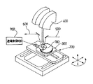
このイオン注入装置は、この不純物注入用マスク100と、このイオン注入用マスク100に被処理基板300の位置合わせを行うXYθステージを有する基板支持台200と、イオン源400とを具備し、イオン源400からこの不純物注入用マスク100を介して、被処理基板300にイオン注入を行うものである。マスクアライメントはこの位置合わせ用光源500およびCCDカメラ600によってなされる。この不純物注入用マスク100は、図1に示したようにメンブレン部にペルチェ素子を形成するとともに、通電制御部700によってメンブレン部が所望の温度を維持できるように、このペルチェ素子への通電量を調整している。800はマスク支持部である。
【0064】
位置合わせについてはアライメント用光学系500を用いて不純物注入用マスクの周縁部に形成された開口Aを介して被処理基板10に形成されたアライメントマークに対して位置合わせを行うことができるようになっている。
なお、イオン源400は、高エネルギー用ECRイオン源と高電流用バーナスイオン源など、異なる2つ以上のイオン源を着脱自在に装着して形成するようにすれば、容易に所望のイオン注入を実現することが可能となる。
【0065】
このイオン注入装置を用いて図8に示すように素子分離用絶縁膜12の形成されたシリコン基板11にイオン注入を行い不純物領域13を形成する。
【0066】
この方法によれば図18(a)乃至(e)に示した従来例の方法との比較からあきらかなように、イオン注入工程の前に必要であったレジストパターンの形成も、イオン注入工程の後に必要であった剥離も不要であり、大幅な工程の簡略化をはかることができる。また、極めてクリーンな環境で効率よくイオン注入を行うことができる。
【0067】
また、この方法によれば、p型不純物イオンを注入してpウェルを形成した後、マスクを取り替え、n型不純物イオンを注入しnウェルを形成するという工程をレジストパターンの形成なしに行うことができるため、このイオン注入装置から被処理基板を取り出すことなく、マスクの取替えのみで効率よく順次異なる導電型のイオンを注入することが可能となる。
【0068】
このようにしてイオン注入を行う際のドーズ量とマスク表面の温度との関係を図9に示す。この図から明らかなように、本発明によれば、イオン注入中、マスク表面に形成したペルチェ素子によってマスク表面を冷却しているため、温度上昇もなくマスクを維持することが出来る。従って、点Aに示すようにマスクの反りも歪もなく、高精度にパターン制御のなされたイオン注入パターンを形成することが可能となる。
【0069】
これに対し、ペルチェ素子を駆動することなく、同一条件でイオン注入を行った場合、図9に線Bで示すように、マスクとウェハの距離が上昇している。このためマスクに反りが生じ、パターン誤差が生じていることがわかる。
【0070】
(第2の実施の形態)
次に、第2の実施の形態について説明する。
この例では、イオン注入用のマスクの基板表面に形成した温度センサにより、マスク表面の温度を測定しながら、イオン注入用マスクの表面温度を一定に維持するようにしたことを特徴とする。
【0071】
このイオン注入用マスクは、図10に示すように、ペルチェ素子100PEを構成するp型不純物領域5およびn型不純物領域4と同一工程で形成したpn接合を用いた温度センサ100cであり、このセンサに流れる電流と両端間電位差とを測定することにより温度差を測定するようにしたものである。半導体のPN接合に順方向に定電流を流したときの両端間電位差の温度依存性は半導体基板の物性によりほぼ決定され、シリコンの場合約-2mV/℃である。温度センサに定電流を流しその両端の電位差を測定することにより温度変化を容易にモニタすることができる。
【0072】
かかる構成によれば、同一基板上に温度制御用のペルチェ素子100PEを構成するpn接合部と、同一工程で形成したセンサ部100Cでマスク表面の温度を測定しているため、高精度の温度制御が可能となり、パターン誤差のないフォトマスクを得ることが可能となる。
【0073】
(第3の実施の形態)
次に、第3の実施の形態について説明する。
この例では、イオン注入用マスクのpn接合部を大きくしたパターンの一例について説明する。図11に示すように、比較的深く形成されたウェル領域35の中に櫛歯状の比較的浅い拡散パターン34を形成したもので、これによりpn接合面の面積は前記第1の実施の形態で説明した例に比べ大幅に増大することができる。
ここで、36Pはウェル側コンタクト、36Nは櫛歯側コンタクトである。
【0074】
この例では、pn接合部の面積を最大限に大きくとることができるため、効率よく温度制御を行うことが可能となる。
【0075】
(第4の実施の形態)
次に、第4の実施の形態について説明する。
この例では、図12に示すように、イオン注入用マスクのpn接合部を深さ方向に形成したものである。
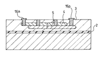
この構成では、基板表面から所定の深さに、n型不純物領域4を形成するとともにさらにその下層にpn接合面を形成するようにp型不純物領域5を形成し,端子16a、16bにより電流を流して接合面を冷却するように構成したものである。
このときp型領域とn型領域の関係は領域4がp型領域5がn型でもよい。
【0076】
これにより、パターン形成面上でpn接合を均一に形成することができ、面内での温度のばらつきを低減することができる。
【0077】
次にこのイオン注入用マスクの製造方法について説明する。
図13(a)乃至(b)はこの製造工程を示す図である。
まず、前記1の実施の形態で説明したのと同様に、直接接合法などにより、シリコン基板1表面に形成された酸化シリコン膜2を介してノンドープシリコン基板を接合し、所望の厚さに研磨することにより、ノンドープシリコン層3を形成する(SOI基板の形成)。
【0078】
このSOI基板を出発材料とし、図13(a)に示すように、ノンドープシリコン層3の所定の深さにpn接合面を形成するように、まずレジストパターン(図示せず)をマスクとしてp型の不純物イオンを注入し、p型不純物領域5を形成する。次に別のレジストパターン(図示せず)をマスクとしてn型の不純物イオンを注入し、n型不純物領域4を形成する。
【0079】
そして、このレジストパターンRを剥離除去し、1000℃、30秒程度のRTA等の活性化を行ったのち、続いて、図13(b)に示すように、更にコンタクト形成用のレジストパターンRを形成し、RIEでコンタクトホールを形成してアルミニウムなどの金属電極をコンタクトホール内に充填する。ことによりコンタクト層7が形成される。
なお、コンタクト層に代えて、高濃度不純物領域で構成してもよい。この場合はそれぞれp型不純物領域およびn型不純物領域にコンタクトするように、順次p側のコンタクト層7およびn側にコンタクト層7を形成する。
【0080】
その後、あらたにマスクパターン形成用のレジストパターンを形成し、酸化シリコン膜2をエッチングストッパとして、RIEによりエッチングを行い、ホールhを形成する。
【0081】
そしてコンタクト層7にアルミニウム層等の配線層を形成し、端子16a、16bを形成する。
【0082】
最後に、図12に示したように裏面にレジストパターン(図示せず)を形成し、これをマスクとして、エッチングを行い、メンブレン部を構成する肉薄領域を形成する。このエッチング工程でも酸化シリコン膜2をエッチングストッパとして用いることにより、オーバーエッチングを防ぎ、制御性よく高精度にパターンを形成することができる。
このときp型領域とn型領域の関係は逆でもよい。
【0083】
このようにして不純物注入用マスクが形成される。
【0084】
(第5の実施の形態)
次に、第5の実施の形態について説明する。
前記実施の形態では、メンブレン部100mを構成する面にpn接合を形成し、冷却を行うようにしたが、この例では、図14に示すようにイオン注入用マスクのメンブレン部に部分支持部100Sを残し、この支持部にpn接合部を形成して、冷却を行うようにしたものである。
【0085】
製造に際しては、シリコン基板の裏面側にイオン注入によりp型不純物領域およびn型不純物領域を形成しておくようにし、メンブレン部形成のためのエッチング工程において、枠状の支持部とともにこの部分支持部を残すようなレジストパターンを形成し、エッチングを行うことによって形成される。
【0086】
このpn接合部は、部分支持部内の深部に、前記メンブレン部の表面と平行な面に形成されているようにすれば、メンブレン表面近傍のイオンビーム不純物の残留によるpn接合特性への影響を受けにくい、より長寿命の信頼性の高いステンシルマスクを提供することが可能となる。
【0087】
(第6の実施の形態)
次に、第6の実施の形態について説明する。
前記第5の実施の形態では、支持部100Sに面に平行なpn接合面を形成したが、この例では図15に示すように、支持部100Sに面に垂直なpn接合面を形成したものである。
他部については前記第5の実施の形態と同様である。
【0088】
この例では、pn接合部は、部分支持部内に、メンブレン部の表面と垂直な面上に形成されているため、微細加工を施すことで、接合周囲長をより長くすることができ、冷却効率の高いマスクを提供することが可能となるという効果がある。
【0089】
(第7の実施の形態)
次に、第7の実施の形態について説明する。
なお、複数のパターン領域で構成したマスクの場合にも適用可能である。図16に示すように、パターンによっては多数のパターン領域に分割し、支持部100Sによって支持された複数のメンブレン部100mを格子状に形成しても良い。100nは枠状の支持部である。この場合は、ウェハのダイシング領域がこの支持部に相当するように形成すれば、プロセスへの影響はなく、収率のよいウェハ処理が可能となる。
【0090】
(第8の実施の形態)
次に、第8の実施の形態について説明する。
なお、パターンによっては形成できないような形状があるが、この場合は図17(a)乃至(c)に示すように、分割形状をなすようにしてもよい。
【0091】
従って、このようにして形成されたステンシルマスクを用いて、フォトリソグラフィ工程を経ることなく作業性よく連続的に、高精度の不純物プロファイルを得ることが可能となる。
【0092】
【発明の効果】
以上説明してきたように、本発明によれば、高精度で信頼性の高いマスクを形成することが可能となる。
【0093】
また本発明によれば、通常のシリコン等を用いた半導体プロセスによって容易に高精度のマスクを形成することが可能となる。
【0094】
本発明の半導体装置の製造方法によれば、レジストパターンの形成工程や、パターン露光工程、レジストパターンの剥離工程を経ることなくイオン注入領域等の形成を容易に行うことが可能となる。
【0095】
また、異なる導電型のイオンを注入する場合にも、同一チャンバー内で真空を破ることなく連続的に注入することができ、作業性が極めて良好であるとともに、汚染の恐れもなく、信頼性の高い半導体装置の提供が可能となる。
【図面の簡単な説明】
【図1】本発明の第1の実施の形態で用いられるマスクを示す図
【図2】本発明の第1の実施の形態で用いられるマスクを示す図
【図3】同マスクの説明図
【図4】同マスクの断面図
【図5】同マスクの製造工程図
【図6】同マスクを用いたイオン注入装置を示す図である。
【図7】本発明の第1の実施の形態のイオン注入方法を示す図である。
【図8】本発明の第1の実施の形態のイオン注入方法を示す図である。
【図9】本発明の第1の実施の形態のイオン注入方法を用いた場合のドーズ量とマスクの変位との関係を示す図である。
【図10】本発明の第2の実施の形態のマスクを示す図である。
【図11】本発明の第3の実施の形態のマスクを示す図である。
【図12】本発明の第4の実施の形態のマスクを示す図である。
【図13】本発明の第4の実施の形態のマスクの製造工程を示す図である。
【図14】本発明の第5の実施の形態のマスクを示す図である。
【図15】本発明の第6の実施の形態のマスクを示す図である。
【図16】本発明の第7の実施の形態のマスクを示す図である。
【図17】本発明の第8の実施の形態のマスクを示す図である。
【図18】従来例のイオン注入方法を示す図である。
【図19】従来例のイオン注入工程におけるステンシルマスクの変形を示す図である。
【図20】同ステンシルマスクの変形におけるマスクパターンのずれを示す説明図である。
【図21】メンブレン部温度とビームパワーとの関係を示す図である。
【図22】マスクのたわみ量とビームパワーとの関係を示す図である。
【符号の説明】
1 シリコン基板
2 酸化シリコン膜
3 ノンドープシリコン層
4 n型不純物領域
5 p型不純物領域
6 アルミニウム配線
6N,6P コンタクト
6C ペルチェ用メタル
7 コンタクト領域
10 被処理基板
R レジスト
100 マスク
100p マスクパターン部
100m メンブレン部
100n 状の支持部部
100c 温度測定部
100S 支持部
101 パッド
500 位置合わせ用光源
600 CCDカメラ
700 通電制御部
800 マスク支持部[0001]
TECHNICAL FIELD OF THE INVENTION
The present invention relates to a mask, a method of manufacturing the same, a method of manufacturing a semiconductor device using the same, and a semiconductor manufacturing apparatus. More particularly, the present invention relates to reduction of distortion due to an increase in temperature of a mask during a processing step.
[0002]
[Prior art]
In recent years, while miniaturization and high integration of semiconductor devices have been progressing, a technique for performing sub-quarter micron processing with high accuracy and high reproducibility has been required.
[0003]
For example, when a semiconductor integrated circuit (LSI) is formed, several to ten times of ion implantation steps are performed in an LSI forming process such as formation of a well, formation of a channel portion, formation of a source / drain region, and formation of a contact region. Need. Usually, a resist is applied to the substrate surface, selective exposure is performed, a resist pattern is formed by photolithography through a development process, and ion implantation is performed through the resist pattern, thereby ion-implanting the opening region of the resist pattern. Is made.
[0004]
For example, FIGS. 18A to 18E show an example of this ion implantation step. As shown in FIG. 18A, an element isolation
[0005]
Thereafter, as shown in FIG. 18B, exposure is performed through a photomask to form a photosensitive region, and as shown in FIG. 18C, the resist in the photosensitive region is removed by development, and the resist pattern is removed. Form R.
[0006]
Then, as shown in FIG. 18D, ion implantation is performed via the resist pattern R to form an
[0007]
Finally, the resist pattern R is removed, and thermal diffusion is performed to form an ion implantation region 13 (diffusion region) having a desired depth as shown in FIG.
[0008]
As described above, it is often necessary to perform resist coating, patterning by exposure / development, and stripping after ion implantation, which requires many steps, and involves a wet process, so that contamination of the substrate surface becomes a serious problem. ing.
In the case where a pattern is formed through such a lithography process, since exposure is performed through a pattern once baked on an exposure mask, a decrease in accuracy due to transfer is also a problem.
[0009]
Meanwhile, a stencil mask has been proposed for an exposure apparatus for charged particles, electron beams, or the like, which is one of the semiconductor manufacturing techniques.
The direct writing technique of scanning an electron beam or the like and directly writing a fine pattern on a wafer (semiconductor substrate) requires an extremely long processing time. Therefore, scanning the electron beam or the like according to the pattern is stopped, and a mask having an opening pattern ( By using a stencil mask and selectively irradiating a wafer (semiconductor substrate) with an electron beam or the like, the processing time is reduced.
[0010]
When this mask technique is applied to an ion implantation technique, an ion beam can be selectively introduced into a wafer (substrate) by using a stencil mask without using a resist mask during ion implantation. This reduces the number of steps such as patterning by resist coating, exposure, and development, and resist stripping after ion implantation, and at the same time eliminates the WET step, eliminating contamination on the wafer surface and enabling a short time pattern formation process. Become.
[0011]
However, in this case, since the mask is irradiated with ions directly, the mask temperature is greatly increased, the mask constituent material is greatly expanded, and warpage and distortion are generated, thereby deteriorating the pattern accuracy. There is a problem.
[0012]
FIGS. 20A and 20B schematically show the displacement of the stencil mask M at normal temperature and at high temperature. At a high temperature, the displacement d (deflection of the mask) is large, and it can be seen that the deviation between the opening position and the opening accuracy of the pattern is extremely large.
[0013]
For example, as shown in Fig. 19, 30mm Two Ion implantation was performed on the surface of the wafer (semiconductor substrate) through a stencil mask M with a thermocouple K at the center of the 10 μm thick membrane section, and the results of measuring the temperature rise of the stencil mask and the displacement (deflection) of the membrane section were measured. This is shown in FIGS.
The ion implantation conditions at this time are boron energy of 90 keV and dose amount of 2E13ions / cm. Two Then, the injection was performed while changing the beam power.
[0014]
As is clear from FIGS. 21 and 22, it can be seen that the temperature of the stencil mask is greatly increased by the beam injection, and the displacement is generated.
As described above, the conventional technique has a problem that a stencil mask cannot form a pattern with high accuracy.
[0015]
This problem is the same not only in technologies involving ions such as ion implantation and ion beam etching, but also in the exposure process of charged particles and electron beams, the etching process and the film formation process. It can be seen that a large temperature change also poses a major problem.
[0016]
The present invention has been made in view of the above circumstances, and has as its object to provide a highly accurate and highly reliable mask without warping or deformation.
[0017]
Another object of the present invention is to provide a (stencil) mask capable of performing high-accuracy ion implantation in an ion implantation technique.
[0018]
It is another object of the present invention to provide a mask for a semiconductor processing step capable of forming a high-precision pattern.
[0019]
It is another object of the present invention to provide a method of manufacturing a mask which is easy to manufacture and has high reliability.
[0020]
It is another object of the present invention to provide a highly accurate and highly reliable ion implantation method and an ion implantation apparatus without requiring the formation of a resist pattern.
[0021]
It is another object of the present invention to provide a highly accurate and highly reliable etching method or film forming method without forming a resist pattern.
[0022]
[Means for Solving the Problems]
Therefore, the mask of the present invention includes a plate-shaped body having a mask pattern portion and a pn junction portion, and a current supply portion for supplying current to the pn junction portion. The Peltier effect is generated, and the temperature of the mask pattern portion can be controlled.
[0023]
According to the present invention, the temperature of the mask itself is controlled by causing a current to flow through the pn junction to generate the Peltier effect. That is, when a current is applied to the pn junction in a direction from the n-type region to the p-type region, electrons move from the junction surface (the electrode on the side) to the n-type region and pass through the n-type region. The energy is absorbed from the electrode on the bonding surface side and is going to pass therethrough, and the energy is released and passed to the electrode (the current-carrying electrode) on the other end side of the n-type region. On the other hand, holes move from the bonding surface (electrode on the side) to the p-type region, absorb energy for passing through the p-type region from the electrode on the bonding surface side, and try to pass the energy. This energy is released and passed to the side electrode (the conducting electrode). As a result, energy is insufficient on the bonding surface side, and the temperature is lowered. Therefore, by controlling the direction or amount of current applied to the pn junction, it is possible to adjust the heat transport and adjust the mask temperature to a desired temperature. Since this can be easily controlled by electrical control, high-precision temperature adjustment is possible, and it is possible to prevent the pattern on the mask from being shifted and to realize high-precision pattern formation.
[0024]
According to the present invention, particularly for a mask used for an application in which a temperature rise due to ion collision is likely to occur, such as a mask for ion implantation, if the mask pattern portion is configured to be a coolable surface by the Peltier effect, This is particularly effective because warpage and distortion can be prevented and a highly reliable pattern can be formed.
[0025]
In particular, if this plate-like body is provided with a thin membrane portion having a mask pattern portion and a frame-like support portion formed on the periphery of the membrane portion, handling is easy. In the case of forming a CMOS device, it is necessary to form a p-well and an n-well, but two steps of forming a resist pattern are required. That is, in the conventional method, the resist is removed after performing ion implantation through a resist coating / patterning step for implanting impurity ions of one conductivity type. After that, a resist coating and patterning step for implanting conductive impurity ions is performed, and then ion implantation is performed to remove the resist. Therefore, it is necessary to pass the wafer through the wet process many times, and there are many causes of contamination when the wafer is taken in and out of the chamber.
[0026]
However, if the mask of the present invention is used, the mask can be freely attached and detached in a processing apparatus such as an ion implantation apparatus by grasping the supporting portion. Accordingly, the mask can be replaced with good workability, and ion implantation can be sequentially performed a plurality of times, thereby greatly improving workability.
[0027]
Desirably, if the membrane portion and the support portion are formed of a single semiconductor substrate, temperature control is facilitated by heat conduction, and generation of distortion due to heat can be suppressed.
[0028]
Further, if the membrane portion is formed of a silicon substrate, it becomes possible to easily and accurately form a pn junction by a normal semiconductor process. Further, even when used as a mask in a semiconductor process, it does not become a cause of contamination in a processing apparatus such as an ion implantation apparatus because it is the same element as an object to be processed.
[0029]
The pn junction is formed of a striped p-type impurity region and an n-type impurity region formed on the surface of the plate-like body so as to be parallel to each other, and the pn junction is perpendicular to the surface of the membrane portion. When formed on a smooth surface, by performing microfabrication, the perimeter of the junction can be lengthened, and there is an effect that a mask with high temperature control efficiency can be provided.
[0030]
Further, as shown in FIG. 11, if the pn junction is formed by a relatively shallow diffusion pattern of a comb-like shape in a well region formed relatively deep on the surface of the plate-like body, Area can be maximized, and the temperature can be controlled efficiently.
[0031]
When the pn junction is formed at a predetermined depth from the surface of the plate and parallel to the surface, the pn junction exists at a uniform density with respect to the surface, so that the temperature distribution in the plane direction is made uniform. At the same time, a pn junction is formed in a deep part, so that a mask having a stable temperature control characteristic and high reliability is less likely to be affected by the residual ion beam impurities near the surface of the membrane. It becomes possible.
[0032]
Desirably, by forming a temperature detecting portion composed of a pn junction on a silicon substrate constituting a mask, temperature detection can be performed with high accuracy, and efficient temperature control can be performed efficiently. .
[0033]
Further, if the pn junction of the temperature detecting section is formed of an impurity region formed in the same step as the diffusion layer constituting the pn junction of the membrane section, high-accuracy temperature detection can be performed more easily. . Further, since the temperature can be controlled efficiently, it is possible to form a highly accurate mask without warpage or distortion.
[0034]
Desirably, if the temperature detecting section is formed on the surface of a supporting section (beam or frame) formed so as to be thicker than the membrane section, it is possible to provide a mask that is stable in strength.
[0035]
Further, if the pn junction is formed in the mask pattern portion, the temperature of the mask pattern formation portion, which is a region where a temperature change is likely to actually occur during the processing step, can be detected with high accuracy. Accurate temperature control becomes possible, and a mask without displacement or deformation can be provided.
[0036]
The pn junction is formed in a region other than the opening of the membrane, and is formed in a partial support (beam) having substantially the same thickness as the frame-shaped support. Therefore, the temperature control unit is formed, so that a mask having high rigidity and high reliability can be formed.
[0037]
Further, if the pn junction is formed in the partial support (beam) in a plane parallel to the surface at a deep portion of the membrane, the pn junction due to the residual ion beam impurities near the surface of the membrane is provided. It is possible to provide a longer-life mask that is less affected by characteristics.
[0038]
Furthermore, if the pn junction is formed on the surface perpendicular to the surface of the membrane portion in the partial support portion (beam), the perimeter of the junction is lengthened by performing fine processing. Therefore, there is an effect that a mask having high cooling efficiency can be provided.
[0039]
In addition, if the membrane portion is formed of a silicon carbide substrate, it can be a mask with less deformation even with relatively inaccurate current control and temperature control, so that it is a highly reliable mask with a simpler configuration. be able to.
[0040]
Furthermore, if the membrane portion is made of a diamond substrate, it is hard and hard to be sputtered, and is stable, so that it is less likely to cause contamination. In addition, since the thermal conductivity is good and the electrical insulation can be maintained, the degree of freedom in designing a mask is large.
[0041]
Further, in the method for manufacturing a mask according to the present invention, a step of implanting impurity ions into the surface of the semiconductor substrate to form at least one pn junction; a step of forming a pattern portion on the surface of the semiconductor substrate; Forming a current supply unit for supplying current so that the Peltier effect can be generated by energization. Although the pattern portion of this mask is formed of an aggregate of openings, it may be formed of a light or ion transmitting region and a non-transmitting region depending on use conditions, and is not necessarily a hole.
[0042]
According to such a method, it is possible to easily form a mask by a normal thin film process.
[0043]
In the method of manufacturing a semiconductor device according to the present invention, a step of aligning and mounting the mask on the surface of the substrate to be processed and a step of selecting physical or chemical processing for the substrate to be processed through the mask are selected. And a processing step to be performed.
[0044]
According to such a method, a desired pattern can be formed with high accuracy while controlling the temperature of the mask surface using a mask utilizing the Peltier effect without performing a photolithography process. Here, the processing refers to film formation, etching, and modification (photosensitization or implantation), physical processing includes optical processing such as exposure, and sputtering and the like, and chemical processing includes film formation such as CVD. Alternatively, there is an etching process such as RIE.
[0045]
Further, in this processing step, if ion implantation is selectively performed on the surface of the substrate to be processed in a region corresponding to the opening of the mask, a rise in the mask temperature is prevented by using the Peltier effect, and warpage and distortion are reduced. It is possible to perform ion implantation in a state where there is no ion implantation.
[0046]
Still further, the processing step includes mounting a first mask having a desired opening pattern formed on the surface of the substrate to be processed, and mounting the first mask on a surface of the substrate to be processed in a region corresponding to the opening of the first mask. A step of implanting first impurity ions, a step of mounting a second mask instead of the first mask on the surface of the substrate to which the first impurity ions have been implanted, and placing the second mask in an opening of the second mask; Implanting a second impurity ion into the surface of the substrate to be processed in a corresponding region, the ion implantation in the CMOS process is extremely simplified, and a highly accurate and highly reliable impurity region is formed. It becomes possible to form well.
[0047]
Preferably, the processing step includes an exposure step of selectively exposing a resist formed on the surface of the substrate to be processed in a region corresponding to the opening of the mask. That is, the mask is used as an exposure mask for electron beam (EB) exposure or the like. In this configuration, since the mask is always kept at a constant temperature and there is no distortion due to heat, a highly accurate mask pattern can be maintained. . Therefore, since the exposure process which has been drawn by beam scanning can be achieved by whole-surface exposure through a mask, the workability is extremely good, exposure can be performed in a short time, and reproducibility and controllability are high.
[0048]
Desirably, if the processing step includes a step of selectively etching the surface of the substrate to be processed in a region corresponding to the opening of the mask, the etching can be performed without going through a photolithography step. In particular, in the case of vapor phase etching, since a wet process is not required, contamination can be prevented and reliability can be improved.
[0049]
Desirably, if the processing step includes a film forming step of selectively forming a thin film on the surface of the substrate to be processed in a region corresponding to the opening of the mask, neither a photolithography step nor a pattern etching step is required. Thus, a highly reliable pattern can be formed.
[0050]
According to the semiconductor manufacturing apparatus of the present invention, the mask, positioning means for positioning and mounting the mask on the surface of the substrate to be processed, and ions for implanting impurity ions into the surface of the substrate to be processed via the mask An injection means and a control means for controlling energization to the pn junction so that the temperature of the mask is constant are provided.
[0051]
According to such an apparatus, it is possible to form a highly accurate and highly reliable ion implantation region with extremely high workability.
[0052]
When performing the process while controlling the temperature, it is sufficient to measure in advance how much the temperature rises, and it is sufficient to supply the current so that a desired temperature difference can be generated. Temperature control can be performed efficiently, and control at a constant temperature can be realized.
[0053]
BEST MODE FOR CARRYING OUT THE INVENTION
Next, embodiments of the present invention will be described in detail with reference to the drawings.
(First Embodiment)
First, as shown in FIGS. 1 and 2 (FIG. 1 is a perspective view, FIG. 2 is a perspective view from the back), the
[0054]
As shown in the sectional view of the main part of FIG. 4, this impurity implantation mask is formed on the surface of the
The Peltier pattern 6C can perform a Peltier operation if used in a voltage range where the pn junction can be broken down without it. Since the pn junction breaks down even at about 1 V at about 1E15 and about 1 V at about 1E16, the voltage range used as the Peltier element may be determined by the breakdown voltage of the pn junction.
[0055]
Next, a method of manufacturing the impurity implantation mask will be described with reference to FIGS.
First, a non-doped silicon substrate is bonded via a
[0056]
Using this SOI substrate as a starting material, as shown in FIG. 5A, a first resist pattern R1 is formed by photolithography, and n-type impurity ions are formed using the first resist pattern R1 as a mask. Implantation is performed to form an n-
[0057]
Subsequently, as shown in FIG. 5B, the resist pattern R1 is peeled off and removed, and a second resist pattern R2 is formed by using a photolithography method. A p-
[0058]
Then, the resist pattern R2 is peeled off and activated, such as RTA at 1000 ° C. for about 30 seconds, and then, as shown in FIG. A third resist pattern R3 is formed.
[0059]
Thereafter, etching is performed by RIE using the third resist pattern R3 as a mask and the
[0060]
Then, the third resist pattern R3 is removed by etching, and a
[0061]
Then, the
Finally, a resist pattern (not shown) is formed on the back surface, and etching is performed using the resist pattern as a mask to form a membrane (thin film) portion. Also in this etching step, by using the
[0062]
Thus, the
[0063]
Next, an ion implantation method using the
This
The ion implantation apparatus includes: an
[0064]
The alignment can be performed using the alignment
If the
[0065]
As shown in FIG. 8, ion implantation is performed on the
[0066]
According to this method, as is apparent from comparison with the method of the conventional example shown in FIGS. Separation, which is necessary later, is not necessary, and the process can be greatly simplified. In addition, ion implantation can be performed efficiently in an extremely clean environment.
[0067]
According to this method, a step of forming a p-well by implanting p-type impurity ions, replacing a mask, and implanting n-type impurity ions to form an n-well is performed without forming a resist pattern. Therefore, ions of different conductivity types can be sequentially and efficiently implanted only by replacing the mask without taking out the substrate to be processed from the ion implantation apparatus.
[0068]
FIG. 9 shows the relationship between the dose and the temperature of the mask surface when performing ion implantation in this manner. As is clear from this figure, according to the present invention, the mask surface can be maintained without temperature rise because the Peltier element formed on the mask surface cools the mask surface during ion implantation. Therefore, as shown in the point A, there is no warpage or distortion of the mask, and it is possible to form an ion implantation pattern whose pattern is controlled with high accuracy.
[0069]
On the other hand, when the ion implantation is performed under the same conditions without driving the Peltier element, the distance between the mask and the wafer increases as shown by the line B in FIG. Therefore, it can be seen that the mask is warped and a pattern error is caused.
[0070]
(Second embodiment)
Next, a second embodiment will be described.
This example is characterized in that the surface temperature of the ion implantation mask is kept constant while the temperature of the mask surface is measured by the temperature sensor formed on the substrate surface of the ion implantation mask.
[0071]
This ion implantation mask is, as shown in FIG. 10, a
[0072]
According to such a configuration, since the temperature of the mask surface is measured by the pn junction forming the Peltier element 100PE for temperature control on the same substrate and the sensor unit 100C formed in the same process, high-precision temperature control is performed. And a photomask free from pattern errors can be obtained.
[0073]
(Third embodiment)
Next, a third embodiment will be described.
In this example, an example of a pattern in which a pn junction of an ion implantation mask is enlarged will be described. As shown in FIG. 11, a relatively shallow diffusion pattern 34 having a comb-like shape is formed in a well region 35 which is formed relatively deep, whereby the area of a pn junction surface is reduced in the first embodiment. Can be greatly increased as compared with the example described in the above.
Here, 36P is a well side contact, and 36N is a comb tooth side contact.
[0074]
In this example, since the area of the pn junction can be maximized, the temperature can be controlled efficiently.
[0075]
(Fourth embodiment)
Next, a fourth embodiment will be described.
In this example, as shown in FIG. 12, a pn junction of an ion implantation mask is formed in a depth direction.
In this configuration, an n-
At this time, the relationship between the p-type region and the n-type region may be such that the
[0076]
As a result, a pn junction can be formed uniformly on the pattern formation surface, and temperature variations in the surface can be reduced.
[0077]
Next, a method of manufacturing the ion implantation mask will be described.
FIGS. 13A and 13B are diagrams showing this manufacturing process.
First, as described in the first embodiment, a non-doped silicon substrate is bonded via a
[0078]
Using this SOI substrate as a starting material, as shown in FIG. 13 (a), a p-type is first formed using a resist pattern (not shown) as a mask so that a pn junction surface is formed at a predetermined depth of the
[0079]
Then, the resist pattern R is peeled and removed, and activation such as RTA at 1000 ° C. for about 30 seconds is performed. Subsequently, as shown in FIG. 13B, a resist pattern R for contact formation is further formed. Then, a contact hole is formed by RIE, and a metal electrode such as aluminum is filled in the contact hole. Thereby, the contact layer 7 is formed.
Note that a high-concentration impurity region may be used instead of the contact layer. In this case, the p-side contact layer 7 and the n-side contact layer 7 are sequentially formed so as to contact the p-type impurity region and the n-type impurity region, respectively.
[0080]
Thereafter, a resist pattern for forming a mask pattern is newly formed, and etching is performed by RIE using the
[0081]
Then, a wiring layer such as an aluminum layer is formed on the contact layer 7, and the
[0082]
Lastly, as shown in FIG. 12, a resist pattern (not shown) is formed on the back surface, and etching is performed using the resist pattern as a mask to form a thin region constituting the membrane portion. Also in this etching step, by using the
At this time, the relationship between the p-type region and the n-type region may be reversed.
[0083]
Thus, an impurity implantation mask is formed.
[0084]
(Fifth embodiment)
Next, a fifth embodiment will be described.
In the above embodiment, a pn junction is formed on the surface constituting the
[0085]
At the time of manufacture, a p-type impurity region and an n-type impurity region are formed by ion implantation on the back surface side of the silicon substrate. In the etching step for forming the membrane portion, the partial support portion is formed together with the frame-shaped support portion. Is formed by forming a resist pattern that leaves a pattern and performing etching.
[0086]
If this pn junction is formed in a deep portion in the partial support portion and in a plane parallel to the surface of the membrane portion, the pn junction characteristics are affected by the residual ion beam impurities near the surface of the membrane. It is possible to provide a highly reliable stencil mask that is difficult and has a longer life.
[0087]
(Sixth embodiment)
Next, a sixth embodiment will be described.
In the fifth embodiment, the pn junction surface parallel to the surface is formed on the support portion 100S. However, in this example, the pn junction surface perpendicular to the surface is formed on the support portion 100S as shown in FIG. It is.
The other parts are the same as in the fifth embodiment.
[0088]
In this example, since the pn junction is formed on the surface perpendicular to the surface of the membrane in the partial support, the perimeter of the junction can be made longer by performing fine processing, and the cooling efficiency can be improved. There is an effect that it is possible to provide a mask having a high density.
[0089]
(Seventh embodiment)
Next, a seventh embodiment will be described.
Note that the present invention can be applied to a mask including a plurality of pattern regions. As shown in FIG. 16, some patterns may be divided into a large number of pattern areas, and a plurality of
[0090]
(Eighth embodiment)
Next, an eighth embodiment will be described.
There are shapes that cannot be formed depending on the pattern. In this case, as shown in FIGS. 17A to 17C, a divided shape may be formed.
[0091]
Therefore, using the stencil mask thus formed, it is possible to continuously obtain a highly accurate impurity profile with good workability without going through a photolithography process.
[0092]
【The invention's effect】
As described above, according to the present invention, a highly accurate and highly reliable mask can be formed.
[0093]
Further, according to the present invention, a highly accurate mask can be easily formed by a normal semiconductor process using silicon or the like.
[0094]
ADVANTAGE OF THE INVENTION According to the manufacturing method of the semiconductor device of this invention, formation of an ion implantation area | region etc. can be easily performed, without going through a resist pattern formation process, a pattern exposure process, and a resist pattern peeling process.
[0095]
In addition, even when ions of different conductivity types are implanted, they can be continuously implanted in the same chamber without breaking the vacuum, so that workability is extremely good, there is no risk of contamination, and reliability is improved. A high semiconductor device can be provided.
[Brief description of the drawings]
FIG. 1 is a view showing a mask used in a first embodiment of the present invention;
FIG. 2 is a view showing a mask used in the first embodiment of the present invention;
FIG. 3 is an explanatory view of the mask.
FIG. 4 is a sectional view of the mask.
FIG. 5 is a manufacturing process diagram of the mask.
FIG. 6 is a diagram showing an ion implantation apparatus using the same mask.
FIG. 7 is a diagram showing an ion implantation method according to the first embodiment of the present invention.
FIG. 8 is a diagram showing an ion implantation method according to the first embodiment of the present invention.
FIG. 9 is a diagram showing the relationship between the dose and the displacement of the mask when the ion implantation method according to the first embodiment of the present invention is used.
FIG. 10 is a diagram showing a mask according to a second embodiment of the present invention.
FIG. 11 is a diagram showing a mask according to a third embodiment of the present invention.
FIG. 12 is a diagram showing a mask according to a fourth embodiment of the present invention.
FIG. 13 is a diagram illustrating a manufacturing process of the mask according to the fourth embodiment of the present invention.
FIG. 14 is a diagram illustrating a mask according to a fifth embodiment of the present invention.
FIG. 15 is a view showing a mask according to a sixth embodiment of the present invention.
FIG. 16 is a view showing a mask according to a seventh embodiment of the present invention.
FIG. 17 is a view showing a mask according to an eighth embodiment of the present invention.
FIG. 18 is a diagram showing a conventional ion implantation method.
FIG. 19 is a diagram showing a deformation of a stencil mask in an ion implantation step of a conventional example.
FIG. 20 is an explanatory diagram showing a shift of a mask pattern in a deformation of the stencil mask.
FIG. 21 is a diagram illustrating a relationship between a membrane portion temperature and a beam power.
FIG. 22 is a diagram illustrating a relationship between a deflection amount of a mask and a beam power.
[Explanation of symbols]
1 Silicon substrate
2 Silicon oxide film
3 Non-doped silicon layer
4 n-type impurity region
5 p-type impurity region
6 Aluminum wiring
6N, 6P contact
6C Metal for Peltier
7 Contact area
10 Substrate to be processed
R resist
100 mask
100p mask pattern section
100m membrane part
100n-shaped support part
100c Temperature measurement unit
100S support
101 pad
500 Light source for alignment
600 CCD camera
700 energization control unit
800 Mask support
Claims (26)
前記pn接合部に電流供給を行う電流供給部とを具備し、
前記pn接合部に通電することにより、ペルチェ効果を生起し、前記マスクパターン部の温度を制御できるようにしたことを特徴とするマスク。A plate-shaped body provided with a mask pattern portion and a pn junction portion;
A current supply unit for supplying a current to the pn junction,
A mask, wherein a current is applied to the pn junction to generate a Peltier effect and control the temperature of the mask pattern portion.
前記半導体基板表面に開口部を形成しマスクパターン部を形成する工程と、
前記pn接合部に通電して、ペルチェ効果を生起させる電流供給部を形成する工程とを含むことを特徴とするマスクの製造方法。Implanting impurity ions into the surface of the semiconductor substrate to form at least one pn junction;
Forming an opening in the surface of the semiconductor substrate to form a mask pattern portion,
Forming a current supply section for generating a Peltier effect by supplying a current to the pn junction.
前記被処理基板に対し、前記マスクを介して物理的または化学的処理を選択的に施す処理工程とを含むことを特徴とする半導体装置の製造方法。19. A step of mounting the mask according to claim 1 on the surface of the substrate to be processed,
Selectively subjecting the substrate to be processed to physical or chemical treatment via the mask.
前記第1のマスクに代えて第2のマスクを前記第1の不純物イオンの注入された被処理基板表面に装着し,前記第2のマスクの開口部に相当する領域の前記被処理基板表面に第2の不純物イオンを注入する工程とを含むことを特徴とする請求項20に記載の半導体装置の製造方法。In the processing step, a first mask on which a desired opening pattern is formed is mounted on the surface of the substrate to be processed, and a first mask is formed on the surface of the substrate to be processed in a region corresponding to the opening of the first mask. Implanting impurity ions,
A second mask is mounted on the surface of the substrate to be processed into which the first impurity ions have been implanted, instead of the first mask, and a second mask is provided on the surface of the substrate to be processed in a region corresponding to an opening of the second mask. 21. The method according to claim 20, further comprising the step of implanting a second impurity ion.
前記マスクを被処理基板表面に位置合わせして装着する位置合わせ手段と、
前記マスクを介して前記被処理基板表面に不純物イオンを注入するイオン注入手段と、
前記マスクの温度が一定となるように前記pn接合部への通電を制御する制御手段とを具備したことを特徴とする半導体製造装置。A mask according to any one of claims 1 to 18,
Positioning means for positioning and mounting the mask on the surface of the substrate to be processed,
Ion implantation means for implanting impurity ions into the surface of the substrate through the mask,
Control means for controlling current supply to the pn junction so that the temperature of the mask is constant.
Priority Applications (5)
| Application Number | Priority Date | Filing Date | Title |
|---|---|---|---|
| JP2002372859A JP2004207385A (en) | 2002-12-24 | 2002-12-24 | Mask, method of manufacturing the same, and method of manufacturing semiconductor device using the same |
| TW092135121A TWI272656B (en) | 2002-12-24 | 2003-12-12 | Mask, method of making same and method of making semiconductor device using same |
| KR1020030092824A KR20040057930A (en) | 2002-12-24 | 2003-12-18 | Mask, method for producing thereof and process for manufacturing semiconductor apparatus using the same |
| US10/741,932 US7344805B2 (en) | 2002-12-24 | 2003-12-18 | Mask and method for producing thereof and a semiconductor device using the same |
| CNB2003101232737A CN100380582C (en) | 2002-12-24 | 2003-12-23 | Mask, manufacturing method thereof, and manufacturing method of semiconductor device using same |
Applications Claiming Priority (1)
| Application Number | Priority Date | Filing Date | Title |
|---|---|---|---|
| JP2002372859A JP2004207385A (en) | 2002-12-24 | 2002-12-24 | Mask, method of manufacturing the same, and method of manufacturing semiconductor device using the same |
Publications (1)
| Publication Number | Publication Date |
|---|---|
| JP2004207385A true JP2004207385A (en) | 2004-07-22 |
Family
ID=32811345
Family Applications (1)
| Application Number | Title | Priority Date | Filing Date |
|---|---|---|---|
| JP2002372859A Pending JP2004207385A (en) | 2002-12-24 | 2002-12-24 | Mask, method of manufacturing the same, and method of manufacturing semiconductor device using the same |
Country Status (5)
| Country | Link |
|---|---|
| US (1) | US7344805B2 (en) |
| JP (1) | JP2004207385A (en) |
| KR (1) | KR20040057930A (en) |
| CN (1) | CN100380582C (en) |
| TW (1) | TWI272656B (en) |
Cited By (3)
| Publication number | Priority date | Publication date | Assignee | Title |
|---|---|---|---|---|
| KR100572949B1 (en) * | 2003-06-30 | 2006-04-28 | 가부시끼가이샤 도시바 | Temperature correction method for heat treatment equipment, adjustment method for development equipment, and manufacturing method of semiconductor device |
| JP2006302528A (en) * | 2005-04-15 | 2006-11-02 | Ulvac Japan Ltd | Ion implantation apparatus and ion implantation method |
| JP2016031947A (en) * | 2014-07-25 | 2016-03-07 | 株式会社東芝 | Semiconductor device manufacturing method and semiconductor manufacturing apparatus |
Families Citing this family (10)
| Publication number | Priority date | Publication date | Assignee | Title |
|---|---|---|---|---|
| JP2005183577A (en) * | 2003-12-18 | 2005-07-07 | Sony Corp | Exposure apparatus, exposure method, and manufacturing method of semiconductor device |
| US7721594B2 (en) | 2005-07-29 | 2010-05-25 | M-I L.L.C. | Apparatus and method to monitor slurries for waste re-injection |
| JP5663717B2 (en) * | 2005-09-06 | 2015-02-04 | カール ツァイス マイクロスコピー ゲーエムベーハーCarl Zeiss Microscopy Gmbh | Charged particle system |
| US20070262051A1 (en) * | 2006-05-12 | 2007-11-15 | Advanced Chip Engineering Technology Inc. | Method of plasma etching with pattern mask |
| US7846849B2 (en) * | 2007-06-01 | 2010-12-07 | Applied Materials, Inc. | Frequency tripling using spacer mask having interposed regions |
| US7820460B2 (en) * | 2007-09-07 | 2010-10-26 | Varian Semiconductor Equipment Associates, Inc. | Patterned assembly for manufacturing a solar cell and a method thereof |
| US9006688B2 (en) * | 2009-04-08 | 2015-04-14 | Varian Semiconductor Equipment Associates, Inc. | Techniques for processing a substrate using a mask |
| US9076914B2 (en) | 2009-04-08 | 2015-07-07 | Varian Semiconductor Equipment Associates, Inc. | Techniques for processing a substrate |
| US8900982B2 (en) | 2009-04-08 | 2014-12-02 | Varian Semiconductor Equipment Associates, Inc. | Techniques for processing a substrate |
| CN108121164B (en) * | 2016-11-29 | 2020-12-01 | 中芯国际集成电路制造(上海)有限公司 | Photomask heat dissipation device and working method thereof |
Citations (6)
| Publication number | Priority date | Publication date | Assignee | Title |
|---|---|---|---|---|
| JPH01120021A (en) * | 1987-11-02 | 1989-05-12 | Fujitsu Ltd | mask cooling device |
| JPH05226579A (en) * | 1992-02-13 | 1993-09-03 | Nec Corp | Heat-conducting substrate, semiconductor device using the heat-conducting substrate and manufacture of heat-conducting substrate |
| JPH09205058A (en) * | 1996-01-25 | 1997-08-05 | Toppan Printing Co Ltd | Aperture for charged beam exposure |
| JPH1079344A (en) * | 1996-09-04 | 1998-03-24 | Canon Inc | Original plate holding apparatus and exposure apparatus using the same |
| JP2000003881A (en) * | 1998-04-17 | 2000-01-07 | Toshiba Corp | Ion implanter, ion generator, and method of manufacturing semiconductor device |
| JP2002203806A (en) * | 2000-10-31 | 2002-07-19 | Toshiba Corp | Method of manufacturing semiconductor device, stencil mask and method of manufacturing the same |
Family Cites Families (6)
| Publication number | Priority date | Publication date | Assignee | Title |
|---|---|---|---|---|
| US4722597A (en) * | 1984-06-08 | 1988-02-02 | Matsushita Electric Industrial Co., Ltd. | Electrooptic shutter array element |
| JPH08191154A (en) * | 1992-04-17 | 1996-07-23 | Intaadetsuku:Kk | Photoelectric device |
| US6098408A (en) * | 1998-11-11 | 2000-08-08 | Advanced Micro Devices | System for controlling reflection reticle temperature in microlithography |
| US6800933B1 (en) * | 2001-04-23 | 2004-10-05 | Advanced Micro Devices, Inc. | Integrated circuit cooling device |
| KR100427583B1 (en) * | 2002-01-16 | 2004-04-28 | 한국전자통신연구원 | Method for fabricating long wavelength vertical-cavity surface emitting lasers |
| US6806006B2 (en) * | 2002-07-15 | 2004-10-19 | International Business Machines Corporation | Integrated cooling substrate for extreme ultraviolet reticle |
-
2002
- 2002-12-24 JP JP2002372859A patent/JP2004207385A/en active Pending
-
2003
- 2003-12-12 TW TW092135121A patent/TWI272656B/en not_active IP Right Cessation
- 2003-12-18 KR KR1020030092824A patent/KR20040057930A/en not_active Ceased
- 2003-12-18 US US10/741,932 patent/US7344805B2/en not_active Expired - Fee Related
- 2003-12-23 CN CNB2003101232737A patent/CN100380582C/en not_active Expired - Fee Related
Patent Citations (6)
| Publication number | Priority date | Publication date | Assignee | Title |
|---|---|---|---|---|
| JPH01120021A (en) * | 1987-11-02 | 1989-05-12 | Fujitsu Ltd | mask cooling device |
| JPH05226579A (en) * | 1992-02-13 | 1993-09-03 | Nec Corp | Heat-conducting substrate, semiconductor device using the heat-conducting substrate and manufacture of heat-conducting substrate |
| JPH09205058A (en) * | 1996-01-25 | 1997-08-05 | Toppan Printing Co Ltd | Aperture for charged beam exposure |
| JPH1079344A (en) * | 1996-09-04 | 1998-03-24 | Canon Inc | Original plate holding apparatus and exposure apparatus using the same |
| JP2000003881A (en) * | 1998-04-17 | 2000-01-07 | Toshiba Corp | Ion implanter, ion generator, and method of manufacturing semiconductor device |
| JP2002203806A (en) * | 2000-10-31 | 2002-07-19 | Toshiba Corp | Method of manufacturing semiconductor device, stencil mask and method of manufacturing the same |
Cited By (4)
| Publication number | Priority date | Publication date | Assignee | Title |
|---|---|---|---|---|
| KR100572949B1 (en) * | 2003-06-30 | 2006-04-28 | 가부시끼가이샤 도시바 | Temperature correction method for heat treatment equipment, adjustment method for development equipment, and manufacturing method of semiconductor device |
| JP2006302528A (en) * | 2005-04-15 | 2006-11-02 | Ulvac Japan Ltd | Ion implantation apparatus and ion implantation method |
| JP2016031947A (en) * | 2014-07-25 | 2016-03-07 | 株式会社東芝 | Semiconductor device manufacturing method and semiconductor manufacturing apparatus |
| US10008390B2 (en) | 2014-07-25 | 2018-06-26 | Toshiba Memory Corporation | Manufacturing method of semiconductor device and semiconductor manufacturing apparatus |
Also Published As
| Publication number | Publication date |
|---|---|
| KR20040057930A (en) | 2004-07-02 |
| CN1510719A (en) | 2004-07-07 |
| TW200416828A (en) | 2004-09-01 |
| US7344805B2 (en) | 2008-03-18 |
| US20040155204A1 (en) | 2004-08-12 |
| TWI272656B (en) | 2007-02-01 |
| CN100380582C (en) | 2008-04-09 |
Similar Documents
| Publication | Publication Date | Title |
|---|---|---|
| JP4334832B2 (en) | Membrane mask having a large area and method for producing the same | |
| JP2004207385A (en) | Mask, method of manufacturing the same, and method of manufacturing semiconductor device using the same | |
| US7745073B2 (en) | Method for manufacturing a semiconductor device, stencil mask and method for manufacturing a the same | |
| JP4363694B2 (en) | Ion implantation apparatus and method for manufacturing semiconductor device | |
| JP2868491B2 (en) | Photolithographic mask and manufacturing method thereof | |
| JP2001118776A (en) | A transfer type exposure apparatus, a mask holding mechanism used in the apparatus, and a method for manufacturing a semiconductor element. | |
| JP2775503B2 (en) | Manufacturing method of junction gate type field effect transistor | |
| JPH09129895A (en) | Method for manufacturing thin film transistor | |
| JP6658892B2 (en) | Semiconductor device and method of manufacturing the same | |
| KR100523170B1 (en) | Method and Apparatus for Electron Projection Lithography | |
| US10867798B2 (en) | Method of manufacturing semiconductor device | |
| US8198015B2 (en) | Method of forming mask pattern | |
| JP2008004867A (en) | Manufacturing method of semiconductor device | |
| JP2001332556A (en) | Method for manufacturing semiconductor device | |
| JP7384106B2 (en) | Manufacturing method of semiconductor device | |
| JP2004109432A (en) | Silicon structure and method of manufacturing the same | |
| JPS58161342A (en) | Manufacture of semiconductor device | |
| JP2022155345A (en) | Power semiconductor and manufacturing method thereof | |
| JP2002231602A (en) | Electron beam exposure apparatus, electron beam molding member and method of manufacturing the same | |
| JP2000021729A (en) | Transmission mask for charged beam batch exposure and method of manufacturing the same | |
| KR100620225B1 (en) | Semiconductor device manufacturing method | |
| KR20010070115A (en) | Member used for charged beam processing apparatus, mask, electron beam exposure apparatus, method for manufacturing semiconductor device, and method for manufacturing mask | |
| KR20020095434A (en) | Method of manufacturing semiconductor device | |
| JPS5811511B2 (en) | Ion etching method | |
| JPS61163635A (en) | Semiconductor impurity doping device |
Legal Events
| Date | Code | Title | Description |
|---|---|---|---|
| A621 | Written request for application examination |
Free format text: JAPANESE INTERMEDIATE CODE: A621 Effective date: 20050316 |
|
| RD04 | Notification of resignation of power of attorney |
Free format text: JAPANESE INTERMEDIATE CODE: A7424 Effective date: 20060424 |
|
| A977 | Report on retrieval |
Free format text: JAPANESE INTERMEDIATE CODE: A971007 Effective date: 20070601 |
|
| A131 | Notification of reasons for refusal |
Free format text: JAPANESE INTERMEDIATE CODE: A131 Effective date: 20070613 |
|
| A521 | Request for written amendment filed |
Free format text: JAPANESE INTERMEDIATE CODE: A523 Effective date: 20070808 |
|
| A131 | Notification of reasons for refusal |
Free format text: JAPANESE INTERMEDIATE CODE: A131 Effective date: 20071121 |
|
| A521 | Request for written amendment filed |
Free format text: JAPANESE INTERMEDIATE CODE: A523 Effective date: 20080121 |
|
| A02 | Decision of refusal |
Free format text: JAPANESE INTERMEDIATE CODE: A02 Effective date: 20080423 |
|
| A521 | Request for written amendment filed |
Free format text: JAPANESE INTERMEDIATE CODE: A523 Effective date: 20080623 |
|
| A911 | Transfer to examiner for re-examination before appeal (zenchi) |
Free format text: JAPANESE INTERMEDIATE CODE: A911 Effective date: 20080702 |
|
| A912 | Re-examination (zenchi) completed and case transferred to appeal board |
Free format text: JAPANESE INTERMEDIATE CODE: A912 Effective date: 20080725 |