【0001】
【発明の属する技術分野】
本発明は、透光性の支持基板上に有機EL(electro luminescence)素子を配設してなる有機ELパネルの駆動装置に関するものである。
【0002】
【従来の技術】
有機ELパネルとしては、特許文献1に開示されるように、ガラス材料からなるガラス基板(透光性の支持基板)上に、ITO(indium tin oxide)等によって陽極となる透明電極(陽極電極)と、正孔注入層,正孔輸送層,発光層及び電子輸送層からなる有機層と、陰極となるアルミニウム(Al)等の非透光性の背面電極(陰極電極)とを順次積層して積層体である有機EL素子を形成し、この有機EL素子によって所定の発光部を形成し、前記発光部を覆うガラス材料からなる凹部形状の封止部材を前記ガラス基板上に紫外線硬化性接着剤を介して気密的に配設する構造のものが知られている。
【0003】
【特許文献1】
特開2002−8855号公報
【0004】
【発明が解決しようとする課題】
かかる有機ELパネルにおける有機EL素子は、周囲環境の温度(有機EL素子が高温)が高温であると寿命が短くなることが知られている。このような特性を有する有機ELパネルを過酷な条件下にさらされる2輪車や4輪車等の車両用計器として搭載する場合において、高温状態にさらされることが多く、更に寿命を低下させてしまう恐れがある。
【0005】
そこで本発明は、有機EL素子の寿命の改善に寄与する有機ELパネルの駆動回路を提供することを目的とするものである。
【0006】
【課題を解決するための手段】
本発明は、前記課題を解決するため、請求項1に記載の通り、透光性の支持基板上に陽極電極,少なくとも発光層を有する有機層及び陰極電極を順次積層形成してなる有機EL素子に電流を与えることで所定発光を得る有機ELパネルの駆動装置であって、周囲温度を検出する温度検出手段と、前記温度検出手段からの検出信号に基づいて温度データを求めるとともに、前記温度データと任意に設定される設定値とを比較し、この比較結果に基づいて通常輝度を得るための第1の定電流値よりも少なくとも一段階小さな第2の定電流値を前記有機EL素子に与えるように制御する制御手段と、を備えてなるものである。
【0007】
また、請求項2に記載の通り、請求項1に記載の有機ELパネルの駆動装置において、前記制御手段は、周囲温度が所定温度以上の際に前記第2の定電流値を前記有機EL素子に与えるように制御してなるものである。
【0008】
また、請求項3に記載の通り、請求項1もしくは請求項2に記載の有機ELパネルの駆動装置において、前記温度検出手段は、前記有機EL素子の近傍に配設されてなるものである。
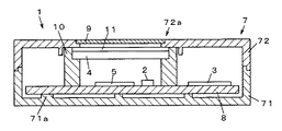
【0009】
【発明の実施の形態】
以下、本発明の実施の形態を添付図面に基づき説明するが、車両に搭載され、車両情報を表示する有機ELパネルの駆動装置を例に挙げ説明する。
【0010】
図1から図3において、駆動装置1は、温度検出手段2と、制御手段3と、駆動回路5とから主に構成され、有機ELパネル4を駆動する。
【0011】
温度検出手段2は、サーミスタから構成され、周囲温度に応じて変化する抵抗値(アナログ信号)を制御手段3に伝達するものである。温度検出手段2は、有機ELパネル5を構成する後述する有機EL素子の温度を検出するべく、有機ELパネル5の近傍に位置するように後述する回路基板上に配設される。
【0012】
制御手段3は、マイクロコンピュータから主に構成され、車両に搭載される車速センサからのSPパルスを入力するとともに、温度検出手段2からのアナログ信号をデジタル信号に変換するA/D変換部を備えた入力部、前記車速センサからのSPパルスに基づいて、所定の演算処理によって車速情報を求めるとともに、温度検出手段2からの前記アナログ信号を入力し、所定の演算処理によって温度情報を求める演算プログラムや前記温度情報に基づく調光プログラムを実行するCPU、前記各プログラムを記憶するROM、所定の設定値が記憶されるEEPROMやバックアップROM等からなる記憶手段、演算結果を一時的に記憶するRAM、前記車速情報に応じた駆動信号を駆動回路5に出力するための出力部等を備えるものである。尚、制御手段3の前記出力部から駆動回路5に出力される駆動信号はPWM信号であり、制御手段3は、前記PWM信号のデューティー比を可変することで有機ELパネル4の表示光の輝度調整を可能とする。
【0013】
有機ELパネル4は、透光性のガラス基板41上に、ITO等によって陽極となる透明電極42と、絶縁層43と、有機層44と、陰極となる非透光性の背面電極45とを順次積層して積層体である有機EL素子46を形成し、有機EL素子46を覆う封止部材47をガラス基板41上に気密的に配設してなるものである。
【0014】
透明電極42は、ガラス基板41上にITO等の導電性材料を蒸着法やスパッタリング法等の手段によって形成されるもので、日の字型の表示セグメント部42aと、個々のセグメントからそれぞれ引き出し形成されたリード部42bと、リード部42bの終端部に設けられる電極部42cとを備えている。尚、電極部42cは、ガラス基板41の一辺に集中的に配設されている。
【0015】
絶縁層43は、例えば、ポリイミド系等の絶縁材料からなり、例えばフォトリソグラフィー法等の手段によって形成される。絶縁層43は、表示セグメント部42aに対応した窓部43aと、背面電極45の後述する電極部に対応する切り欠き部43bとを有し、発光領域の輪郭を鮮明に表示するため、透明電極42の表示セグメント部42aの周縁部と若干重なるように窓部43aが形成され、また、透明電極42と背面電極45との絶縁を確保するためにリード部42b上を覆うように配設される。
【0016】
有機層44は、少なくとも発光層を有するものであれば良いが、本発明の実施の形態においては正孔注入層,正孔輸送層,発光層及び電子輸送層を蒸着法やスパッタリング法等の手段によって順次積層形成してなるものである。有機層44は、絶縁層43における窓部43aの形成箇所に対応するように所定の大きさをもって配設される。
【0017】
背面電極45は、アルミ(Al)やアルミリチウム(Al:Li),マグネシウム銀(Mg:Ag)等の金属性の導電性材料を蒸着法やスパッタリング法等の手段によって形成されるものであり、有機層44上に配設される。背面電極45は、透明電極42における各電極部42cと隣接するようにガラス基板2の一辺に設けられるリード部45aと電気的に接続される。尚、リード部45aの終端部には、電極部45bが設けられ、リード部45a及び電極部45bは透明電極42と同材料により形成される。
【0018】
封止部材47は、例えばガラス材料からなる平板部材に凹部47aを形成してなるものであり、凹部47aを取り囲むように形成される支持部47bのガラス基板41との接合部47cに、紫外線硬化型エポキシ樹脂接着剤(図示しない)を所定量配設し、接合部47cをガラス基板41上に接合することで有機EL素子46を収納する収納空間を気密的に封止する構成である。尚、封止部材47は、透明電極42の電極部42c及び背面電極45の電極部45bが外部に露出するようにガラス基板41よりも若干小さめに構成されている。
【0019】
以上の各部によって有機ELパネル4が構成されるものである。
【0020】
駆動回路5は、制御手段3から発せられるPWM信号に応じた定電流値(駆動信号)を有機ELパネル4に付与するもので、制御手段3からのPWM信号のデューティー比に応じた定電流値を有機ELパネル4に付与する。
【0021】
以上により有機ELパネル4の駆動装置1が構成されるものであるが、かかる駆動装置1はケース体7に収納されるものである。ケース体7は、制御手段3及び駆動回路5や他の電子部品を実装した硬質回路基板8を固定支持する複数の支持体71aを有する下ケース71と、有機ELパネル4からの表示光を外部に発するための開口部72aを有する上ケース72との2分割構造である。尚、上ケース72は、開口部72aを塞ぐように透光性の前面パネル9が接着剤を介して配設されている。
【0022】
また、有機ELパネル4は、枠状のホルダ部材10を介して回路基板8上に配設されるもので、有機ELパネル4は、有機ELパネル4の各電極部42c,45bと電気的に接続されるフレキシブル配線板(図示しない)によって回路基板8と電気的に接続される。また、有機ELパネル4の表示光の出射面側には、前記表示光を良好に視認するための円偏光板11が貼着される。
【0023】
次に、図4及び図5を用いて、有機ELパネル4の駆動装置1の作用について説明する。
【0024】
制御手段3は、有機ELパネル4の近傍に位置するように回路基板8上に配設される温度検出手段2からの入力情報(アナログ信号)に基づいて、有機ELパネル4の周囲の温度情報を得る。制御手段3は、周囲温度が所定温度、例えば60℃以上の高温状態に達したか否かを判定する。制御手段は3は、周囲温度が高温状態に達していない場合、通常駆動電流値(所定輝度を得るための定電流値(第1の定電流値))を駆動回路5を介して有機ELパネルに印加する。また制御手段3は、周囲温度が高温状態に達している場合、通常駆動電流を100%とした場合に70%の駆動電流値(第2の定電流値)を駆動回路5を介して有機ELパネル4に印加する(図4参照)。
【0025】
即ち、制御手段3は、周囲温度が高温状態になると、有機ELパネル4の発光輝度を低下させるべく駆動電流値を調整するものであり、この輝度調整にあっては、通常時の発光輝度を100%とすると、表示光の視認に影響を及ぼさない30%を低減させることが可能な駆動電流値を有機ELパネル4に印加するものである(図5参照)。
【0026】
かかる有機ELパネル4の駆動装置1は、有機ELパネル4に与える駆動電流値を低く保つことで有機EL素子45の寿命が延長できるといった有機EL素子の駆動特性に着目し、有機ELパネル4を取り巻く環境が有機EL素子46の寿命に影響を与える温度に達した場合に通常時よりも低い駆動電流値を印加することで、高温時の有機ELパネル46の劣化促進を抑制することができるため、有機EL素子の寿命の改善に寄与する機ELパネル4の駆動回路1を提供することができる。
【0027】
また、温度検出手段2を有機ELパネル4の近傍である回路基板8に配設することで、有機ELパネル4の温度を正確に検出することが可能となる。
【0028】
尚、前述した実施形態では周囲温度の設定値を60℃としたが、本発明の設定温度は有機EL素子46の寿命に影響を与える温度が好ましく、有機EL素子46を構成する材料によってその温度は異なるため、有機EL素子46の種類により適宜変更する必要がある。
【0029】
また、前述した実施形態では、設定温度を一段階に設定するものであったが、本発明にあっては、設定温度を複数段階に設定し、高温になるに連れて定電流値を次第に小さくするものであっても良い。
【0030】
また、前述した実施形態では、有機ELパネル4をセグメント表示式のものを用いて説明したが、本発明にあっては、複数の陽極ライン(陽極電極)と複数の陰極ライン(陰極電極)とが交差する状態で配設されるとともに、前記陽極ラインと前記陰極ラインとの間に有機層を挟持して発光部をマトリクス状に形成するドットマトリクス型の有機ELパネルに適用しても良い。
【0031】
また、前述した実施形態では、温度検出手段2を有機EL素子46の近傍の回路基板8に配設するものであったが、本発明の温度検出手段2の配設位置は前述の位置に限定されるものではなく、例えば有機ELパネル4におけるガラス基板41や封止部材47に温度検出手段を配設するものであっても良い。
【0032】
【発明の効果】
本発明は、透光性の支持基板上に陽極電極,少なくとも発光層を有する有機層及び陰極電極を順次積層形成してなる有機EL素子に定電流を与えることで所定発光を得る有機ELパネルの駆動装置に関し、有機EL素子の寿命の改善に寄与する機ELパネルの駆動回路を提供することができる。
【図面の簡単な説明】
【図1】本発明の実施形態の有機ELパネルの駆動装置を示すブロック図。
【図2】同上実施形態の有機ELパネルの斜視図。
【図3】同上実施形態の有機ELパネルの駆動装置の要部断面図。
【図4】同上実施形態の有機ELパネルの温度に対する駆動電流を示す図。
【図5】同上実施形態の有機ELパネルの温度に対する発光輝度を示す図。
【符号の説明】
1 駆動装置
2 温度検出手段
3 制御手段
4 有機ELパネル
41 ガラス基板(支持基板)
42 透明電極(陽極電極)
44 有機層
45 背面電極(陰極電極)
46 有機EL素子
5 駆動回路[0001]
TECHNICAL FIELD OF THE INVENTION
The present invention relates to a driving apparatus for an organic EL panel in which an organic EL (electro luminescence) element is provided on a light-transmitting support substrate.
[0002]
[Prior art]
As disclosed in Patent Document 1, as an organic EL panel, a transparent electrode (anode electrode) serving as an anode by indium tin oxide (ITO) or the like on a glass substrate (translucent support substrate) made of a glass material. And an organic layer including a hole injection layer, a hole transport layer, a light emitting layer, and an electron transport layer, and a non-transparent back electrode (cathode electrode) such as aluminum (Al) serving as a cathode. An organic EL device as a laminate is formed, a predetermined light emitting portion is formed by the organic EL device, and a concave sealing member made of a glass material covering the light emitting portion is provided on the glass substrate with an ultraviolet curable adhesive. There is known a device having a structure in which the device is hermetically disposed via a cable.
[0003]
[Patent Document 1]
JP-A-2002-8855
[Problems to be solved by the invention]
It is known that the life of the organic EL element in such an organic EL panel is shortened when the temperature of the surrounding environment (the temperature of the organic EL element is high) is high. When an organic EL panel having such characteristics is mounted as an instrument for a vehicle such as a two-wheeled vehicle or a four-wheeled vehicle that is exposed to severe conditions, it is often exposed to a high temperature, and the life is further reduced. There is a risk of getting it.
[0005]
Therefore, an object of the present invention is to provide a driving circuit of an organic EL panel that contributes to improvement of the life of the organic EL element.
[0006]
[Means for Solving the Problems]
According to an aspect of the present invention, there is provided an organic EL device comprising: an anode, an organic layer having at least a light-emitting layer, and a cathode; A driving device for an organic EL panel that obtains predetermined light emission by applying a current to the device, comprising: a temperature detecting means for detecting an ambient temperature; and obtaining temperature data based on a detection signal from the temperature detecting means; And a set value arbitrarily set, and a second constant current value at least one step smaller than the first constant current value for obtaining normal luminance is provided to the organic EL element based on the comparison result. Control means for performing the control as described above.
[0007]
According to a second aspect of the present invention, in the driving device for an organic EL panel according to the first aspect, the control means changes the second constant current value when the ambient temperature is equal to or higher than a predetermined temperature. Is controlled so as to be given.
[0008]
According to a third aspect of the present invention, in the driving device for an organic EL panel according to the first or second aspect, the temperature detecting means is provided near the organic EL element.
[0009]
BEST MODE FOR CARRYING OUT THE INVENTION
Hereinafter, an embodiment of the present invention will be described with reference to the accompanying drawings. A drive device of an organic EL panel mounted on a vehicle and displaying vehicle information will be described as an example.
[0010]
1 to 3, a driving device 1 mainly includes a temperature detecting unit 2, a control unit 3, and a driving circuit 5, and drives an organic EL panel 4.
[0011]
The temperature detecting means 2 is constituted by a thermistor, and transmits a resistance value (analog signal) which changes according to the ambient temperature to the control means 3. The temperature detecting means 2 is provided on a circuit board described later so as to be located near the organic EL panel 5 so as to detect a temperature of an organic EL element described later constituting the organic EL panel 5.
[0012]
The control means 3 mainly includes a microcomputer, and has an A / D converter for inputting an SP pulse from a vehicle speed sensor mounted on the vehicle and converting an analog signal from the temperature detecting means 2 into a digital signal. An input program for obtaining vehicle speed information by predetermined arithmetic processing based on the SP pulse from the vehicle speed sensor and inputting the analog signal from the temperature detecting means 2 to obtain temperature information by predetermined arithmetic processing. A CPU that executes a dimming program based on the temperature information, a ROM that stores the programs, a storage unit that includes an EEPROM or a backup ROM that stores a predetermined set value, a RAM that temporarily stores a calculation result, And an output unit for outputting a drive signal corresponding to the vehicle speed information to the drive circuit 5. The drive signal output from the output section of the control means 3 to the drive circuit 5 is a PWM signal, and the control means 3 varies the duty ratio of the PWM signal to change the luminance of the display light of the organic EL panel 4. Allows adjustment.
[0013]
The organic EL panel 4 includes a transparent electrode 42 serving as an anode made of ITO or the like, an insulating layer 43, an organic layer 44, and a non-light-transmitting back electrode 45 serving as a cathode formed on a translucent glass substrate 41. The organic EL element 46 as a laminate is formed by successively laminating, and a sealing member 47 covering the organic EL element 46 is disposed on the glass substrate 41 in an airtight manner.
[0014]
The transparent electrode 42 is formed by depositing a conductive material such as ITO on the glass substrate 41 by a method such as a vapor deposition method or a sputtering method. And an electrode portion 42c provided at the end of the lead portion 42b. Note that the electrode portions 42c are intensively arranged on one side of the glass substrate 41.
[0015]
The insulating layer 43 is made of, for example, a polyimide-based insulating material, and is formed by, for example, a photolithography method. The insulating layer 43 has a window portion 43a corresponding to the display segment portion 42a and a cutout portion 43b corresponding to an electrode portion of the back electrode 45 which will be described later. A window 43a is formed so as to slightly overlap the periphery of the display segment 42a of 42, and is disposed so as to cover the lead 42b in order to ensure insulation between the transparent electrode 42 and the back electrode 45. .
[0016]
The organic layer 44 may have at least a light emitting layer. In the embodiment of the present invention, the hole injection layer, the hole transport layer, the light emitting layer, and the electron transport layer are formed by a method such as an evaporation method or a sputtering method. Are sequentially formed. The organic layer 44 is provided with a predetermined size so as to correspond to the location where the window 43 a is formed in the insulating layer 43.
[0017]
The back electrode 45 is formed of a metallic conductive material such as aluminum (Al), aluminum lithium (Al: Li), and magnesium silver (Mg: Ag) by a method such as an evaporation method or a sputtering method. It is provided on the organic layer 44. The back electrode 45 is electrically connected to a lead portion 45a provided on one side of the glass substrate 2 so as to be adjacent to each electrode portion 42c of the transparent electrode 42. An electrode portion 45b is provided at the end of the lead portion 45a, and the lead portion 45a and the electrode portion 45b are formed of the same material as the transparent electrode 42.
[0018]
The sealing member 47 is formed by forming a concave portion 47a on a flat plate member made of, for example, a glass material. A predetermined amount of a type epoxy resin adhesive (not shown) is provided, and the joining portion 47c is joined to the glass substrate 41 to hermetically seal the accommodation space for accommodating the organic EL element 46. The sealing member 47 is configured to be slightly smaller than the glass substrate 41 so that the electrode portion 42c of the transparent electrode 42 and the electrode portion 45b of the back electrode 45 are exposed to the outside.
[0019]
The organic EL panel 4 is configured by the above components.
[0020]
The drive circuit 5 applies a constant current value (drive signal) corresponding to the PWM signal emitted from the control unit 3 to the organic EL panel 4, and the constant current value according to the duty ratio of the PWM signal from the control unit 3. Is applied to the organic EL panel 4.
[0021]
The driving device 1 of the organic EL panel 4 is configured as described above. The driving device 1 is housed in the case body 7. The case body 7 includes a lower case 71 having a plurality of supports 71a for fixedly supporting the rigid circuit board 8 on which the control means 3 and the drive circuit 5 and other electronic components are mounted, and externally transmits display light from the organic EL panel 4. This is a two-part structure with the upper case 72 having an opening 72a for emitting light. The upper case 72 is provided with a light-transmitting front panel 9 via an adhesive so as to cover the opening 72a.
[0022]
The organic EL panel 4 is disposed on the circuit board 8 via a frame-shaped holder member 10. The organic EL panel 4 is electrically connected to the electrode portions 42c and 45b of the organic EL panel 4. It is electrically connected to the circuit board 8 by a connected flexible wiring board (not shown). In addition, a circularly polarizing plate 11 for adhering the display light satisfactorily is adhered on the emission surface side of the display light of the organic EL panel 4.
[0023]
Next, the operation of the driving device 1 for the organic EL panel 4 will be described with reference to FIGS.
[0024]
The control means 3 controls the temperature information around the organic EL panel 4 based on the input information (analog signal) from the temperature detecting means 2 provided on the circuit board 8 so as to be located near the organic EL panel 4. Get. The control means 3 determines whether or not the ambient temperature has reached a predetermined temperature, for example, a high temperature state of 60 ° C. or higher. When the ambient temperature has not reached the high temperature state, the control means 3 sends the normal drive current value (a constant current value (first constant current value) for obtaining a predetermined luminance) via the drive circuit 5 to the organic EL panel. Is applied. Further, when the ambient temperature has reached a high temperature state, the control means 3 supplies a drive current value (second constant current value) of 70% (second constant current value) to the organic EL via the drive circuit 5 when the normal drive current is 100%. Apply to panel 4 (see FIG. 4).
[0025]
That is, when the ambient temperature becomes high, the control means 3 adjusts the drive current value so as to reduce the light emission luminance of the organic EL panel 4. Assuming that it is 100%, a drive current value capable of reducing 30% which does not affect the visibility of display light is applied to the organic EL panel 4 (see FIG. 5).
[0026]
The driving device 1 for the organic EL panel 4 focuses on the driving characteristics of the organic EL element such that the life of the organic EL element 45 can be extended by keeping the driving current value given to the organic EL panel 4 low, and When the surrounding environment reaches a temperature that affects the life of the organic EL element 46, by applying a drive current value lower than normal, it is possible to suppress the promotion of deterioration of the organic EL panel 46 at high temperatures. Thus, it is possible to provide the driving circuit 1 for the device EL panel 4 which contributes to the improvement of the life of the organic EL element.
[0027]
In addition, by disposing the temperature detecting means 2 on the circuit board 8 near the organic EL panel 4, it is possible to accurately detect the temperature of the organic EL panel 4.
[0028]
In the above-described embodiment, the set value of the ambient temperature is set to 60 ° C. However, the set temperature of the present invention is preferably a temperature that affects the life of the organic EL element 46, and the set temperature depends on the material constituting the organic EL element 46. Therefore, it is necessary to appropriately change the type according to the type of the organic EL element 46.
[0029]
In the above-described embodiment, the set temperature is set in one step. However, in the present invention, the set temperature is set in a plurality of steps, and the constant current value is gradually reduced as the temperature increases. It may be something to do.
[0030]
In the above-described embodiment, the organic EL panel 4 is described as a segment display type. However, in the present invention, a plurality of anode lines (anode electrodes) and a plurality of cathode lines (cathode electrodes) are used. May be arranged in an intersecting manner, and may be applied to a dot matrix type organic EL panel in which an organic layer is sandwiched between the anode line and the cathode line to form a light emitting portion in a matrix.
[0031]
In the above-described embodiment, the temperature detecting means 2 is disposed on the circuit board 8 near the organic EL element 46. However, the position of the temperature detecting means 2 of the present invention is limited to the above-described position. Instead, for example, a temperature detecting means may be provided on the glass substrate 41 or the sealing member 47 in the organic EL panel 4.
[0032]
【The invention's effect】
The present invention relates to an organic EL panel that obtains a predetermined light emission by applying a constant current to an organic EL element formed by sequentially laminating an anode electrode, an organic layer having at least a light emitting layer, and a cathode electrode on a translucent support substrate. With respect to the driving device, it is possible to provide a driving circuit for the EL panel, which contributes to the improvement of the life of the organic EL element.
[Brief description of the drawings]
FIG. 1 is a block diagram showing a driving device of an organic EL panel according to an embodiment of the present invention.
FIG. 2 is a perspective view of the organic EL panel of the embodiment.
FIG. 3 is a sectional view of a main part of the driving device of the organic EL panel according to the embodiment.
FIG. 4 is a diagram showing a driving current with respect to a temperature of the organic EL panel according to the embodiment.
FIG. 5 is a view showing light emission luminance with respect to temperature of the organic EL panel of the embodiment.
[Explanation of symbols]
REFERENCE SIGNS LIST 1 drive device 2 temperature detection means 3 control means 4 organic EL panel 41 glass substrate (support substrate)
42 Transparent electrode (anode electrode)
44 Organic layer 45 Back electrode (cathode electrode)
46 Organic EL Element 5 Drive Circuit