JP2004226830A - Liquid crystal display and electronic equipment - Google Patents
Liquid crystal display and electronic equipment Download PDFInfo
- Publication number
- JP2004226830A JP2004226830A JP2003016219A JP2003016219A JP2004226830A JP 2004226830 A JP2004226830 A JP 2004226830A JP 2003016219 A JP2003016219 A JP 2003016219A JP 2003016219 A JP2003016219 A JP 2003016219A JP 2004226830 A JP2004226830 A JP 2004226830A
- Authority
- JP
- Japan
- Prior art keywords
- liquid crystal
- layer
- display device
- crystal display
- retardation
- Prior art date
- Legal status (The legal status is an assumption and is not a legal conclusion. Google has not performed a legal analysis and makes no representation as to the accuracy of the status listed.)
- Pending
Links
- 239000004973 liquid crystal related substance Substances 0.000 title claims abstract description 274
- 239000000758 substrate Substances 0.000 claims abstract description 59
- 150000001875 compounds Chemical class 0.000 claims abstract description 25
- 239000007788 liquid Substances 0.000 claims description 8
- 239000005264 High molar mass liquid crystal Substances 0.000 abstract description 36
- 239000010410 layer Substances 0.000 description 191
- 230000005540 biological transmission Effects 0.000 description 20
- 238000010586 diagram Methods 0.000 description 17
- 239000011241 protective layer Substances 0.000 description 16
- 230000000052 comparative effect Effects 0.000 description 13
- 238000000034 method Methods 0.000 description 12
- 238000011156 evaluation Methods 0.000 description 9
- 210000002858 crystal cell Anatomy 0.000 description 6
- 230000000694 effects Effects 0.000 description 6
- 239000000178 monomer Substances 0.000 description 6
- 239000000463 material Substances 0.000 description 5
- 239000007921 spray Substances 0.000 description 5
- SECXISVLQFMRJM-UHFFFAOYSA-N N-Methylpyrrolidone Chemical compound CN1CCCC1=O SECXISVLQFMRJM-UHFFFAOYSA-N 0.000 description 4
- NIXOWILDQLNWCW-UHFFFAOYSA-N acrylic acid group Chemical group C(C=C)(=O)O NIXOWILDQLNWCW-UHFFFAOYSA-N 0.000 description 4
- 210000004027 cell Anatomy 0.000 description 4
- 230000003287 optical effect Effects 0.000 description 4
- 239000011347 resin Substances 0.000 description 4
- 229920005989 resin Polymers 0.000 description 4
- 230000007704 transition Effects 0.000 description 4
- ZWEHNKRNPOVVGH-UHFFFAOYSA-N 2-Butanone Chemical compound CCC(C)=O ZWEHNKRNPOVVGH-UHFFFAOYSA-N 0.000 description 3
- 239000011521 glass Substances 0.000 description 3
- 238000005286 illumination Methods 0.000 description 3
- 239000011159 matrix material Substances 0.000 description 3
- 238000005259 measurement Methods 0.000 description 3
- 230000010363 phase shift Effects 0.000 description 3
- 230000010287 polarization Effects 0.000 description 3
- 230000000630 rising effect Effects 0.000 description 3
- 238000004088 simulation Methods 0.000 description 3
- 239000000243 solution Substances 0.000 description 3
- 238000004528 spin coating Methods 0.000 description 3
- YEJRWHAVMIAJKC-UHFFFAOYSA-N 4-Butyrolactone Chemical compound O=C1CCCO1 YEJRWHAVMIAJKC-UHFFFAOYSA-N 0.000 description 2
- 239000004642 Polyimide Substances 0.000 description 2
- JHIVVAPYMSGYDF-UHFFFAOYSA-N cyclohexanone Chemical compound O=C1CCCCC1 JHIVVAPYMSGYDF-UHFFFAOYSA-N 0.000 description 2
- AMGQUBHHOARCQH-UHFFFAOYSA-N indium;oxotin Chemical compound [In].[Sn]=O AMGQUBHHOARCQH-UHFFFAOYSA-N 0.000 description 2
- 229910052751 metal Inorganic materials 0.000 description 2
- 239000002184 metal Substances 0.000 description 2
- 239000004033 plastic Substances 0.000 description 2
- 229920001721 polyimide Polymers 0.000 description 2
- 229920000642 polymer Polymers 0.000 description 2
- 239000000126 substance Substances 0.000 description 2
- 239000000956 alloy Substances 0.000 description 1
- 229910045601 alloy Inorganic materials 0.000 description 1
- 229910052782 aluminium Inorganic materials 0.000 description 1
- XAGFODPZIPBFFR-UHFFFAOYSA-N aluminium Chemical compound [Al] XAGFODPZIPBFFR-UHFFFAOYSA-N 0.000 description 1
- 230000015572 biosynthetic process Effects 0.000 description 1
- 239000011248 coating agent Substances 0.000 description 1
- 238000000576 coating method Methods 0.000 description 1
- 239000000470 constituent Substances 0.000 description 1
- 239000013078 crystal Substances 0.000 description 1
- 230000006866 deterioration Effects 0.000 description 1
- 230000005684 electric field Effects 0.000 description 1
- 238000005516 engineering process Methods 0.000 description 1
- 238000007654 immersion Methods 0.000 description 1
- 150000002576 ketones Chemical class 0.000 description 1
- 239000011259 mixed solution Substances 0.000 description 1
- 239000012046 mixed solvent Substances 0.000 description 1
- 239000003960 organic solvent Substances 0.000 description 1
- 230000001681 protective effect Effects 0.000 description 1
- 230000035945 sensitivity Effects 0.000 description 1
- 229910052709 silver Inorganic materials 0.000 description 1
- 239000004332 silver Substances 0.000 description 1
- 239000002904 solvent Substances 0.000 description 1
Images


Landscapes
- Polarising Elements (AREA)
- Liquid Crystal (AREA)
Abstract
【課題】表示輝度の改善、及び視野角の改善、並びにバックライト光の利用効率の改善を実現した表示品質に優れる反射型、あるいは半透過反射型の液晶表示装置を提供する。
【解決手段】互いに対向して配置された上基板と下基板の間に、TNモードの液晶層16が挟持され、前記液晶層の上基板側に上偏光板が設けられた液晶表示装置において、前記下基板の内面側に設けられた、有限のチルト角を有して配向された液晶性化合物を主体とする位相差層20を構成する高分子液晶20aのダイレクタ20dが、平面視において当該液晶表示装置の明視方向と略平行かつ略逆向きに配向されている
【選択図】 図2An object of the present invention is to provide a reflective or transflective liquid crystal display device having improved display luminance, improved viewing angle, and improved use efficiency of backlight light, and having excellent display quality.
In a liquid crystal display device, a TN mode liquid crystal layer 16 is sandwiched between an upper substrate and a lower substrate that are arranged to face each other, and an upper polarizing plate is provided on the upper substrate side of the liquid crystal layer. A director 20d of a polymer liquid crystal 20a constituting a retardation layer 20 mainly composed of a liquid crystal compound oriented at a finite tilt angle and provided on the inner surface side of the lower substrate is a liquid crystal in plan view. It is oriented substantially parallel and substantially opposite to the clear viewing direction of the display device.
Description
【0001】
【発明の属する技術分野】
本発明は、液晶表示装置及び電子機器に関し、特に、特に、半透過反射型の液晶表示装置であって、反射モードのみならず、透過モード時にも十分に明るい表示が可能な優れた視認性を有する液晶表示装置の構成に関するものである。
【0002】
【従来の技術】
従来から、明るい場所では、通常の反射型の液晶表示装置と同様に外光を利用し、暗い場所では、内部の光源により表示を視認可能にした液晶表示装置が提案されている。この液晶表示装置は、反射型と透過型を兼ね備えた表示方式を採用しており、周囲の明るさに応じて反射表示または透過表示のいずれかの表示方式に切り替えることにより、消費電力を低減しつつ周囲が暗い場合でも明瞭な表示を行うことができる。
【0003】
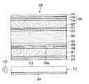
図15は、この種の半透過反射膜を用いた半透過反射型液晶表示装置の一例を示す断面構造図であり、本出願人により出願された特許文献1に記載の構成を有する液晶表示装置である。
この液晶表示装置100では、一対のガラス基板101,102間に液晶層103が挟持されており、下基板101の内面に、開口部104aを有する半透過反射層104、インジウム錫酸化物(Indium Tin Oxide, 以下、ITOと略記する)等の透明導電膜からなる透明電極108が積層され、透明電極108を覆うように配向膜107が形成されている。一方、上基板102の内面には、ITO等の透明導電膜からなる透明電極112が形成され、この透明電極112を覆うように配向膜113が形成されている。また、上基板102の外面側には、上基板102側から順に2枚の位相差板118、119(これら位相差板は1/4波長板120として機能する)、上偏光板114が配置され、下基板101の外面側には、1/4波長板115、下偏光板116がこの順に設けられている。また、光源122、導光板123、反射板124等からなるバックライト117(照明手段)が下偏光板116の下方に配置されている。なお、1/4波長板115,120は、ある波長帯域において直線偏光をほぼ円偏光にすることができるものである。
【0004】
上記構成の液晶表示装置100によれば、外光の有無に関わらず表示の視認が可能ではあるものの、反射表示に比べて透過表示の明るさが不足するという問題があった。その原因の一つは、バックライト117から出射された光のうち、半透過反射層104の開口部104aを通過しない光は、半透過反射層104の裏面で反射されると、回転方向が反転した円偏光となり、1/4波長板115を透過すると下偏光板116の透過軸と垂直な直線偏光になる。そして、この直線偏光が下偏光板116によって吸収されることになり、バックライトから出射された光の利用効率が低くなってしまうことにある。
【0005】
これに対して、特許文献2に記載の、液晶パネルの内面側に円偏光層を設けた構成では、バックライト光の利用効率を高めることが可能になっている。この円偏光層は、特定の回転方向の円偏光を透過し、逆回りの円偏光を反射する特性を有する光学層であり、上記円偏光層で反射された光をバックライト側へ戻して再利用するようになっている。さらに、係る文献には、上記円偏光層の液晶層側に液晶性化合物からなる位相差層を設け、円偏光層を透過した光を直線偏光に変換することで直線偏光による表示を行う構成が開示されている。
【0006】
【特許文献1】
特許第3235102号公報
【特許文献2】
特開平9−258210号公報
【0007】
【発明が解決しようとする課題】
上記特許文献2に記載の技術を特許文献1に記載の液晶表示装置に適用すれば、バックライト光の利用効率を向上させることができ、表示の明るさを改善できると考えられる。しかしながら、係る効果が得られるのは半透過反射型液晶表示装置の透過表示領域に限ってである。また、特許文献2にも反射型、あるいは半透過反射型の液晶表示装置に適用するための記載はなされていない。
【0008】
本発明は、上記事情に鑑みて成されたものであって、表示輝度の改善、及び視野角の改善、並びにバックライト光の利用効率の改善を実現した表示品質に優れる反射型、あるいは半透過反射型の液晶表示装置を提供することを目的としている。
【0009】
【課題を解決するための手段】
本発明は、上記目的を達成するために以下の構成の液晶表示装置、及び電子機器を提供する。
本発明の液晶表示装置は、互いに対向して配置された上基板と下基板の間に、TNモードの液晶層が挟持された液晶表示装置において、前記液晶層の上基板側に上偏光板が設けられ、前記下基板の内面側に、基板側から順に反射層と、有限のチルト角を有して配向された液晶性化合物を主体とする位相差層とが設けられており、前記位相差層を構成する液晶性化合物のダイレクタが、平面視において当該液晶表示装置の明視方向と略平行かつ略逆向きに配向されていることを特徴とする。
【0010】
本発明に係る液晶表示装置は、反射表示を行うための反射層の液晶層側に位相差層を備えており、かつ位相差層を構成する液晶性化合物のダイレクタが、当該液晶表示装置の明視方向に対して上記方位関係となるように配置されていることで、反射表示における視角特性を改善し、広い視角で高コントラストの表示が得られるようになっている。尚、本発明者は上記位相差層の高分子液晶の配向方向が適切であることを、試作した液晶表示装置を用いて検証しており、その詳細は(実施例)の項に記載している。
尚、上記液晶性化合物のダイレクタの方向は、液晶層を構成する液晶分子のダイレクタと同様に、液晶性化合物の長手方向に沿って、水平面から上基板側に起きあがる方向を指すベクトルの方向を指す。また、上記明視方向は、TNモードの液晶層においては、その層厚方向ほぼ中央に配置された液晶分子のダイレクタの方向である。
【0011】
次に、本発明の液晶表示装置は、互いに対向して配置された上基板と下基板の間に、TNモードの液晶層が挟持され、1ドット領域内に透過表示領域と反射表示領域とを有する半透過反射型液晶表示装置において、前記液晶層の上基板側に上偏光板が設けられ、前記下基板の内面側の前記反射表示領域に基板側から順に反射層と、有限のチルト角を有して配向された液晶性化合物を主体とする位相差層とが設けられており、前記位相差層を構成する液晶性化合物のダイレクタが、平面視において当該液晶表示装置の明視方向と略平行かつ略逆向きに配向されており、選択電圧印加時、非選択電圧印加時のいずれか一方において、前記透過表示領域における前記液晶層の位相差が前記反射表示領域における前記液晶層の位相差よりも大きいことを特徴とする。
【0012】
上記構成は、前記の反射型液晶表示装置の構成を、半透過反射型液晶表示装置に適用したものであり、その反射表示領域において、反射層上に位相差層が設けられ、位相差層を構成する高分子液晶のダイレクタが、当該液晶表示装置の明視方向と平面視略平行かつ略逆向きとされている。係る構成の液晶表示装置によれば、反射表示において広い視角範囲で高コントラストの表示が得られ、かつ従来の半透過反射型液晶表示装置の透過表示の輝度が不足するという問題点も解決できるものである。
【0013】
すなわち、上記構成では、下基板の内面の反射表示領域にのみ位相差層を設け、この位相差層の存在により反射表示領域にのみ位相差が付加されるのを補償すべく、透過表示領域での液晶層の位相差を反射表示領域での液晶層の位相差よりも大きくされている。この構成においては、位相差層、液晶層の位相差等の設定条件によって透過表示において直線偏光のみで表示を行うことが可能となり、下側の位相差板のみならず、上側の位相差板も不要とすることができる。その結果、従来の構成において円偏光の略半分が上偏光板で吸収されることで透過表示が暗くなる問題を解決することができ、従来に比べて透過表示を明るくすることができる。また、従来に比べて構造が簡単になり、装置の薄型化を図ることができる。なお、本発明の液晶表示装置の表示原理については(発明の実施の形態)の項で説明する。
【0014】
本発明の液晶表示装置では、前記位相差層を構成する液晶性化合物が、チルト構造を成して配向されており、前記液晶性化合物の平均チルト角が、2°以上35°以下であることが好ましい。上記平均チルト角が2°未満では、視角の改善効果がほとんど得られない。また、35°を越えるチルト角では、視角特性が低下する。具体的には、液晶表示装置の正面でコントラストが最大とならずに、斜め方向から視認した場合にコントラストが最大となるため、観察者に視認される実質的なコントラストが低下することになる。また、上記35°を越えるチルト角では、駆動電圧が上昇する傾向になるため、消費電力の点からも好ましくない。
【0015】
本発明の液晶表示装置では、前記位相差層を構成する液晶性化合物の平均チルト角が、10°以上25°以下であることが好ましい。
このような構成とすることで、液晶表示装置正面の観察者左右方向で対称な視角特性を有する、特に視認性に優れた液晶表示装置が得られる。
【0016】
また本発明の液晶表示装置では、前記位相差層を構成する液晶性化合物が、スプレイ構造を成して配向されている構成とすることもできる。
上記構成であっても、本発明の液晶表示装置は、広い視角で明るい表示が得られる。
【0017】
本発明の液晶表示装置では、前記透過表示領域における液晶層厚が、前記反射表示領域における液晶層厚よりも大きいことが好ましい。このような構成とすることで、液晶層を透過する光に対する複屈折作用を、透過表示領域と反射表示領域とで近づけることができ、表示コントラストの改善を図ることができる。
【0018】
本発明の液晶表示装置では、前記透過表示領域における液晶層厚が、前記反射表示領域における液晶層厚の略2倍であることが好ましい。
すなわち、透過表示領域での液晶層の位相差を反射表示領域での液晶層の位相差よりも大きくする手段としては、例えば液晶層の厚さをd、液晶の屈折率異方性をΔnとしたときに、複屈折位相差(リタデーション)はこれらの積Δn・dで表されるので、液晶層の厚さd、液晶の屈折率異方性Δnの少なくともいずれか一方を透過表示領域と反射表示領域とで異ならせればよい。しかしながら、実際には透過表示領域と反射表示領域で液晶の屈折率異方性Δnを大きく変えるのは困難なので、透過表示領域における液晶層の層厚を反射表示領域における液晶層の層厚よりも大きく設定することが容易である。
上記構成はいわゆるマルチギャップ構造を備えた液晶表示装置であり、本発明の液晶表示装置に係る構成を導入するすることで、透過表示領域における液晶層の実質的リタデーションと反射表示領域の実質的リタデーションを容易に揃えることができ、高コントラストの液晶表示装置を実現できる。
【0019】
本発明の液晶表示装置では、前記反射表示領域における液晶層のΔndが、0.13以上0.34以下であることが好ましい。上記範囲とすることで、高輝度、高コントラストの反射表示が得られる。上記範囲を超えると、輝度及びコントラストが低下する傾向になり好ましくない。
【0020】
本発明の液晶表示装置では、前記位相差層が、透過光に対して略1/4波長の複屈折位相差を付与するものとされていることが好ましい。
上記構成とすることで、例えば透過表示領域の液晶層のリタデーションを1/2波長とし、反射表示領域のリタデーションを1/4波長とした場合に、反射表示と透過表示とで上偏光板の透過時の偏光状態を略同一方向の直線偏光に揃えることができ、また反射表示領域におけるリタデーションと透過表示領域におけるリタデーションを略等しくされるので、光の利用効率を最も向上でき、透過表示が最も明るい構成とすることができる。また、コントラストの高い表示を得ることができる。
【0021】
次に、本発明の電子機器は、先に記載の本発明の液晶表示装置を備えたことを特徴とする。係る構成によれば、透過表示、反射表示のいずれにおいても高輝度、高コントラストの表示が得られ、かつ広視野角の反射表示が得られる表示部を備えた電子機器を提供することができる。
【0022】
【発明の実施の形態】
以下、本発明の実施の形態を図面を参照して説明する。
図1は本実施の形態の液晶表示装置の概略構成を示す断面図であり、図2はその表示原理を説明するための図であって、表示原理の説明に必要な構成要素のみを示す図である。また、本実施の形態はアクティブマトリクス方式の半透過反射型カラー液晶表示装置の例である。なお、以下の全ての図面においては、図面を見やすくするため、各構成要素の膜厚や寸法の比率などは適宜異ならせてある。
【0023】
本実施の形態の液晶表示装置10は、図1に示すように、液晶セル11とバックライト12(照明装置)とを備えたものである。液晶セル11は、下基板13と上基板14とが対向配置され、これら上基板14と下基板13と挟まれた空間にTN(Twisted Nematic)液晶等が封入されて液晶層16が形成されている。そして、液晶セル11の後面側(下基板13の外面側)にバックライト12が配置されている。
【0024】
ガラスやプラスチックなどの透光性材料からなる下基板13の内面側には、アルミニウム、銀、またはこれらの合金等の反射率の高い金属膜からなる半透過反射層18が形成されている。半透過反射層18には、バックライト12から出射された光を透過させるための開口部18aが各画素毎に設けられており、半透過反射層18の形成領域のうち、実際に金属膜が存在している部分が反射表示領域R、開口部18aの部分が透過表示領域Tを構成している。
【0025】
反射表示領域Rにおける半透過反射層18上には、位相差層20と、保護層21とが基板側から順次積層されている。位相差層20は例えば高分子液晶等の液晶性化合物から構成され、係る位相差層20を透過する光に対して1/4波長の複屈折位相差を付与するものである。保護層21は、例えばアクリル系感光性樹脂等の絶縁膜から構成されている。
【0026】
これら位相差層20および保護層21は、例えば以下の2通りの方法によって形成することができる。
第1の方法は、まず最初に、半透過反射層18を形成した基板上に配向膜材料であるSE−3140(商品名、日産化学(株)製)をスピンコート法、あるいはフレキソ印刷法で塗布、焼成した後、ラビング処理を行う。次に、この配向膜上に高分子液晶溶液をスピンコート法(例えば回転数700rpmで30秒)により塗布する。ここで用いる高分子液晶は、例えばPLC−7023(商品名、旭電化工業(株)製)の8%溶液であり、溶媒はシクロヘキサノンとメチルエチルケトンの混合液、アイソトロピック転移温度が170℃、屈折率異方性Δnが0.21のものである。
【0027】
次に、高分子液晶層のプレベイクを80℃で1分間行い、さらに高分子液晶のアイソトロピック転移温度(170℃)以上となる180℃で30分間加熱した後、徐々に冷却して高分子液晶を配向させる。本発明者らがこの条件で実際に製造したところ、膜厚は630nm、位相差は133nmが得られている。
【0028】
次に、保護層の材料としてアクリル系感光性樹脂NN−525(商品名、JSR(株)製)をスピンコート法(例えば回転数700rpmで30秒)で塗布する。このとき、膜厚は2.3μmであった。次に、保護層のプレベイクを80℃で3分間行った後、フォトマスクを用いた露光(例えば露光強度が140mJ/cm2、350nmに感度を持つ紫外線光量計で測定した値)を行い、アルカリ性現像液中に室温で90秒浸漬して現像を行い、反射表示領域にのみ保護層を残存させる。なお、上記のアクリル系感光性樹脂はネガ型のため、反射表示領域が露光されるようにフォトマスクを形成しておく必要がある。
【0029】
次に、保護層を完全に硬化させるため、ポスト露光を露光強度2000mJ/cm2で行う。なお、1000mJ/cm2以下では次工程の高分子液晶の現像時に保護層の剥離が生じたが、1300mJ/cm2以上では問題なかったので、2000mJ/cm2と設定した。次いで、Nメチル−2ピロリジノンからなるエッチング液に室温で30分間浸漬し、高分子液晶のエッチングを行う。次いで、この基板を80℃で3分間乾燥することにより、高分子液晶からなる位相差層20とアクリル系感光性樹脂からなる保護層21が形成される。
【0030】
第2の方法は、第1の方法と同様にして配向膜を形成した基板上に、液晶性モノマーであるUVキュアラブル液晶UCL−008−K1(商品名、大日本インキ化学工業(株)製)の溶液を、スピンコート法(例えば回転数700rpmで30秒)により塗布する。ここで用いる液晶性モノマー溶液は、Nメチル−2ピロリジノンとγ−ブチロラクトンの混合溶媒に25%に希釈したものであり、アイソトロピック転移温度が69℃、屈折率異方性Δnが0.20である。
【0031】
次に、液晶性モノマーを60℃で5分間乾燥させ、アイソトロピック転移温度(69℃)以上となる90℃で5分間加熱した後、徐々に冷却して液晶性モノマーを配向させる。本発明者らがこの条件で実際に製造したところ、膜厚は650nmが得られた。次いで、フォトマスクを用いた露光(例えば露光強度が3000mJ/cm2)を行うことにより液晶性モノマーを局所的に光重合させた後、アルカリ性現像液、もしくはケトン系有機溶剤中に60秒浸漬して現像を行い、反射表示領域にのみ液晶性モノマー重合体を残存させる。これにより、液晶性モノマー重合体からなる位相差層20が形成される。その後、第1の方法と同様に、位相差層20上に保護層21を形成すればよい。
【0032】
このように、本実施の形態の液晶表示装置10においては、反射表示領域Rにのみ位相差層20、保護層21が設けられたことにより、反射表示領域Rと透過表示領域Tとの間に段差が形成されている。そして、この段差に沿ってITO等の透明導電膜からなる画素電極23が形成され、画素電極23を覆うようにポリイミド等からなる配向膜24が積層されている。本実施の形態の場合、下基板13はTFT等の画素スイッチング素子、データ線、走査線等が形成された素子基板から構成されているが、図1においては画素スイッチング素子、データ線、走査線等の図示は省略している。また、下基板13の外面側には下偏光板28が設けられており、従来の位相差板は設けられていない。
【0033】
一方、ガラスやプラスチックなどの透光性材料からなる上基板14の内面側には、ITO等の透明導電膜からなる共通電極32、ポリイミド等からなる配向膜33が順次積層されている。また、上基板14の外面側には上偏光板36が設けられており、従来の位相差板は設けられていない。なお、図示を省略したが、上基板の内面側にはR(赤)、G(緑)、B(青)の各色素層を有するカラーフィルタが設けられている。
【0034】
上基板14と下基板13との間に挟持された液晶層16は、反射表示領域Rのみに位相差層20と保護層21が設けられ、これらの層が液晶層16側に突出するように形成されたことにより、反射表示領域Rと透過表示領域Tとでその層厚が異なっている。本実施の形態の場合、保護層21の膜厚は位相差層20の膜厚の略4倍程度であり、液晶層16の層厚は主に保護層21の膜厚によって調整されている。具体的には、透過表示領域Tの液晶層16の層厚は反射表示領域Rの液晶層16の層厚の略2倍となっている。そして、液晶層16の材料としてポジ型の晶が用いられ、選択電圧印加(電圧オン)時には電界方向に沿って液晶分子が立ち上がり、液晶層16の位相のずれが反射表示領域R、透過表示領域Tともに0となる一方、非選択電圧印加(電圧オフ)時には液晶分子が寝た状態となり、液晶層16のリタデーションが反射表示領域Rでは1/4波長、透過表示領域Tでは1/2波長となるように、液晶の屈折率異方性Δnおよび液晶層厚dが設定されている。上基板14のラビング軸と上偏光板36の透過軸とが垂直または平行であり、液晶層16の液晶分子が、非選択電圧印加時において上基板14と下基板13との間で90°ツイストした状態となっている。
【0035】
また、バックライト12は、光源37と反射板38と導光板39を有しており、導光板39の下面側(液晶パネル1と反対側)には、導光板39中を透過する光を液晶セル11側に向けて出射させるための反射板40が設けられている。
【0036】
上記構成を備えた本実施形態の液晶表示装置は、反射表示領域Rにあたる領域に形成された位相差層20の液晶性化合物のダイレクタと、液晶層16の液晶分子のダイレクタとの方位関係を適切に調整することで、反射表示において広い視角範囲で明るい表示が得られるようになっている。この位相差層20及び液晶層16との関係を、図2の説明図を参照して以下に説明する。
【0037】
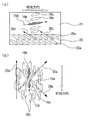
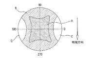
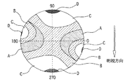
図2(a)は、図1に示す液晶層16と位相差層20とを示す断面構成図であり、図2(b)は、同平面構成図である。これらの図では、上記各層を構成する液晶分子(16a、20a)を模式的に示している。
図2(a)、図2(b)には、液晶層16の非選択電圧印加状態が示されており、液晶層16を構成する液晶分子16aは、図2(a)左右方向に横たわるように配向されており、液晶層16の層厚方向ほぼ中央に位置する液晶分子16bのダイレクタ16dは、水平方向よりやや右上向きとなっている。また、平面的には、図2(b)に示すように、液晶層16を構成する液晶分子16aは、90°にツイスト配向されている。また、同平面図において位相差層20は、チルト構造(図4(a)参照)を成して配向された複数の高分子液晶20aから構成されており、複数の高分子液晶20aは、ほぼ平行に配向されている。また、図2(a)に示すように高分子液晶20aのダイレクタ20dは、図示やや左上向きである。
【0038】
図2(a)、(b)に示すように、本実施形態の液晶表示装置の明視方向は、液晶層16の層厚方向ほぼ中央に配置された液晶分子16bのダイレクタ16dの向きにより決定され、図2(a)の断面視においては、図示右方向とされ、図2(b)の平面視においては、図示下方向とされている。そして、この明視方向に対して、位相差層20のダイレクタ20dは、図2(b)に示すように、平面視略平行かつ逆向きになっている。すなわち、液晶分子16bのダイレクタ16dと、位相差層20の高分子液晶のダイレクタ20dとが、平面視略平行、かつ逆向きに配置されている。
【0039】
また、図2(b)に符号28a、36aで示す矢印は、それぞれ下偏光板28及び上偏光板36の透過軸の向きを示しており、両透過軸28a、36aは互いに直交する向きに配置されている。液晶層16を構成する液晶分子16aのうち、下偏光板28aに隣接して配置された液晶分子のダイレクタは下偏光板28の透過軸28aと略平行とされ、上偏光板36に隣接する液晶分子のダイレクタは上偏光板36の透過軸36aと略平行とされている。従って、本実施形態において、位相差層20aの高分子液晶のダイレクタ20dと、上下偏光板の透過軸28a、36aは、それぞれほぼ45°の角度を成して配置されている。
【0040】
本実施形態の液晶表示装置では、液晶層16を構成する液晶分子16a、16bと、位相差層20を構成する高分子液晶20aとが、上記方位関係を有していることで、広い視角範囲で明るい表示が得られるようになっている。本発明者は、係る構成により高輝度表示が可能な視角範囲が実質的に広がることを実際の液晶表示装置の視角特性を評価することにより検証しており、その詳細は後述の(実施例)に記載している。
【0041】
本実施形態の場合、上記位相差層20の高分子液晶のダイレクタ20dと、明視方向とが、平面視略平行とされ、かつ逆向きとされている。本発明に係る液晶表示装置においては、前記両者が平行に配置されるのが最も好ましいが、前記ダイレクタ20dと、液晶表示装置の明視方向とは、平面視において実質的に逆向きに配置されていれば、平面的に交差する向きであってもよい。具体的には、ダイレクタ20dと、明視方向との交差角度が3°以下であれば、実用上は問題とならない(明視方向を対称軸としてほぼ対称の視角範囲で高輝度の表示が得られる)。また、上記交差角度は1°以下とすることがより好ましい。尚、上記ダイレクタ20dと、明視方向とが平面視において互いに交差する向きとされた場合には、ダイレクタ20dと、偏光板28、36の透過軸との方位関係もそれに準じた交差角度となる。
【0042】
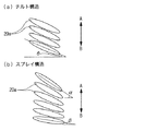
また、図4(a)は、チルト構造を成して配向された液晶分子を示す模式図であり、図4(b)は、スプレイ構造を成して配向された液晶分子を示す模式図である。これらの図に示す矢印が位相差層20の厚さ方向に対応しており、A方向が液晶層16側、B方向が下基板13側である。
先に記載のように、本実施形態では、位相差層20の高分子液晶20aは、図4(a)に示すようなチルト構造に配向されている。本実施形態の場合、図4(a)に示すチルト角θは、2°以上35°以下とされる。チルト角が2°未満では、位相差層20の視角特性の非対称性が小さくなるために、上記視角改善効果がほとんど得られなくなる。また、チルト角が35°を越えると、位相差層の厚さ方向における相対的な光学異方性が大きくなりすぎるために、コントラストが最大となる視角方向が表示装置正面から外れ、観察者に視認される実質的なコントラストが低下するため好ましくない。また、チルト角が35°を越える場合には、光進行方向のズレのために、最適な表示が得られる液晶層16の駆動電圧が大きくなる傾向になり、消費電力の点で不利になる。
【0043】
さらに、本実施の形態では、位相差層20を構成する高分子液晶20aが、チルト構造を成して配向されている場合について説明したが、高分子液晶20aが、図4(b)に示すスプレイ構造を成して配向された構成も適用することができる。その場合にも、各高分子液晶のダイレクタと、液晶表示装置の明視方向とが、平面視において略平行かつ略逆向きとなるように位相差層20を構成することで、上記と同様に広い視角で高コントラストの表示が可能な液晶表示装置とすることができる。
また、図4(b)に示すスプレイ構造において、角度α、βは、それぞれ位相差層20内における高分子液晶20aの仰角の最大値α、及び最小値βを示すものであり、本発明に係る液晶表示装置では、下基板13側で仰角が最小(β)となり、位相差層20の厚さ方向に沿って連続的に仰角が大きくなり、液晶層16側で仰角が最大(α)となる。これらの仰角の最大値α及び最小値βは、それぞれ40°、2°程度とすることが好ましい。その理由は、充分な視角改善効果が得られる平均チルト角10°から25°の範囲であり、また最大値αと最小値βの差を大きくすることでより視角改善の効果が得られるためである。
【0044】
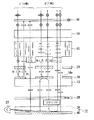
次に、本実施の形態の液晶表示装置10の表示原理を図3を用いて説明する。
まず、暗表示を行う場合には、液晶層16に電圧を印加した状態(選択電圧印加状態)とし、液晶層16でのリタデーションがほぼ0(位相のずれがない)となるようにしておく。反射表示においては、上偏光板36の上方から入射した光は、上偏光板36の透過軸を紙面に垂直とすると、上偏光板36を透過した後、紙面に垂直な直線偏光となり、そのままの状態で液晶層16を透過する。そして、紙面に垂直な直線偏光は、下基板13上の位相差層20により1/4波長のリタデーションが付加され、位相差層20を透過した後、左回りの円偏光となる。次に、この円偏光が半透過反射層18の表面で反射すると回転方向が反転して右回りの円偏光となり、位相差層20を再度透過した後、紙面に平行な直線偏光となり、そのままの状態で液晶層16を透過する。ここで、上偏光板36は紙面に垂直な透過軸を有しているので、紙面に平行な直線偏光は上偏光板36に吸収されて外部(観察者側)へは戻らず、暗表示となる。
【0045】
一方、透過表示においては、バックライト12から出射された光は、下偏光板28の透過軸を紙面に平行とした場合、下偏光板28を透過した後、紙面に平行な直線偏光となり、そのままの状態で液晶層16を透過する。この光は、反射モードと同様、上偏光板36に吸収されるので、暗表示となる。
【0046】
次に、明表示を行う場合には、液晶層16に電圧を印加しない状態(非選択電圧印加状態)とし、反射表示領域Rにおけるリタデーションが1/4波長、透過表示領域Tにおけるリタデーションが1/2波長となるようにする。反射表示においては、上偏光板114を透過した紙面に垂直な直線偏光は、液晶層16により1/4波長のリタデーションが付与されて液晶層16を透過して位相差層20の表面に到達した段階で左回りの円偏光となる。そして、位相差層20を透過した後、紙面に平行な直線偏光となり、半透過反射層18の表面でそのままの偏光状態で反射し、位相差層20を再度透過すると、左回りの円偏光に戻る。次に、この光が液晶層16を再度透過した段階で紙面に垂直な直線偏光に戻り、紙面に垂直な透過軸を有する上偏光板36を透過して外部(観察者側)へ戻り、明表示となる。
【0047】
一方、透過表示においては、バックライト12から出射され、下偏光板28を透過した紙面に平行な直線偏光は、液晶層16の持つ旋光性によって、液晶層16を透過した段階で紙面に垂直な直線偏光となり、紙面に垂直な透過軸を有する上偏光板36を透過して外部へ戻り、明表示となる。
また透過表示において、下偏光板28を透過した紙面に平行な直線偏光のうち、半透過反射層18の裏面で反射した光は、そのまま下偏光板28を透過してバックライト12に戻り、バックライト12下面の反射板40で反射して再度液晶セル11に向けて出射されるので、半透過反射層18の裏面で反射した光を再利用して透過表示に寄与させることができる。
【0048】
本実施の形態の液晶表示装置10においては、下基板13内面の反射表示領域Rにのみ1/4波長のリタデーションを持つ位相差層20を設け、さらに、透過表示領域Tにおける液晶層16の層厚を反射表示領域Rにおける液晶層16の層厚の略2倍とし、電圧無印加時の液晶層16のリタデーションを反射表示領域Rで1/4波長、透過表示領域Tで1/2波長としたことによって、透過表示については直線偏光のみで表示を行うことが可能となり、図15に示す従来の装置で用いていた液晶セルの上下の位相差板をともに不要とすることができる。
【0049】
この構成によれば、従来の構成において液晶層側から入射される円偏光の略半分が上偏光板で吸収されることで透過表示が暗くなる問題、半透過反射層の裏面で反射された照明光が下偏光板で吸収され、表示に再利用できない問題の双方を同時に解決することができるので、従来に比べて透過表示を明るくすることができる。また本実施の形態の場合、特に透過表示領域Tでのリタデーションを反射表示領域Rの2倍としたことにより、反射表示と透過表示とで上偏光板36を透過する前の偏光状態を同一方向の直線偏光に揃えることができるため、光の利用効率を最も向上でき、透過表示が最も明るい構成とすることができる。また、コントラストの高い表示を得ることができる。特に本実施の形態の場合、透過表示が直線偏光を用いたTNモードの表示となるので、光の利用効率が高く、明るい表示が可能であるとともに、視野角も広くすることができる。また、透過表示領域のセル厚がばらついても、更にはかなり厚く反射表示領域のセル厚の2倍以上になっても、旋光性を利用しているため、コントラストの高い表示が可能である。
【0050】
本実施の形態の構成によれば、高分子液晶で位相差層20を形成しているが、その上に絶縁膜を形成しているので、この絶縁膜が保護膜21として機能し、位相差層20の変質等を防止することができる。また、反射表示領域Rにのみ位相差層20を設けているため、その位相差層20上に保護層21を形成したことにより、反射表示領域Rにおける液晶層16の層厚を透過表示領域Tにおける液晶層16の層厚よりも小さくする構造を容易に実現することができる。さらに、外付けの位相差板が要らないので、従来に比べて構造が簡単になり、部品点数を削減できるとともに、装置の薄型化を図ることができる。
【0051】
本発明者は、本実施の形態の液晶表示装置において反射表示領域の位相差(リタデーションR=Δn・d)と反射率との相関関係をシミュレーションにより求めた。シミュレーション結果を図14に示す。図14の横軸はΔn・d[nm]、縦軸は反射率[−]である。本実施の形態の場合、透過表示がTNモードの表示となることから光の利用効率が高く、明るい表示となる一方、反射表示に対しては実用上必要な明るさとして少なくとも反射率20%以上が要求される。このレベルの反射率を得るためには、反射表示領域の位相差(Δn・d)を、130nm≦Δn・d≦340nmの範囲とする必要がある。この条件を満たすように反射表示領域のΔn・dを設定することによって、反射表示の視認性も確保することができる。
【0052】
なお、本発明の技術範囲は上記実施の形態に限定されるものではなく、本発明の趣旨を逸脱しない範囲において種々の変更を加えることが可能である。例えば上記実施の形態では、反射表示領域上の位相差層でのリタデーションを1/4波長とし、透過表示領域の液晶層の層厚を反射表示領域の2倍とすることで選択電圧印加時の液晶層のリタデーションが反射表示領域、透過表示領域ともにほぼ0、非選択電圧印加時の液晶層のリタデーションが反射表示領域で1/4波長、透過表示領域で1/2波長とした。この設定が透過表示を最も明るくし、コントラストが最も向上できる構成ではあるが、各部のリタデーションは必ずしも上記の設定通りでなくても良く、少なくとも反射表示領域にのみ位相差層20によるリタデーションが付与され、そのリタデーションを緩和すべく透過表示領域でのリタデーションが反射表示領域でのリタデーションよりも大きければよい。この構成とすれば、少なくとも従来に比べて透過表示を明るくすることができる。
【0053】
また、上記実施の形態ではポジ型液晶を用い、初期状態を水平配向として電圧印加時のリタデーションがほぼ0、電圧無印加時に反射表示領域のリタデーションが1/4波長、透過表示領域のリタデーションが1/2波長となる例で説明したが、これとは逆に、ネガ型液晶を用い、初期状態を垂直配向として電圧無印加時に位相のずれがほぼ0、電圧印加時に反射表示領域のリタデーションが1/4波長、透過表示領域のリタデーションが1/2波長となるように構成することもできる。さらに、本発明は、上記実施の形態のようにアクティブマトリクス方式の半透過反射型カラー液晶表示装置に限ることなく、パッシブマトリクス方式、白黒表示の液晶表示装置に適用することも可能である。
【0054】
(電子機器)
図16は、本発明に係る液晶表示装置を表示部に備えた電子機器の一例である携帯電話の斜視構成図であり、この携帯電話1300は、本発明の液晶表示装置を小サイズの表示部1301として備え、複数の操作ボタン1302、受話口1303、及び送話口1304を備えて構成されている。
上記実施の形態の液晶表示装置は、上記携帯電話に限らず、電子ブック、パーソナルコンピュータ、ディジタルスチルカメラ、液晶テレビ、ビューファインダ型あるいはモニタ直視型のビデオテープレコーダ、カーナビゲーション装置、ページャ、電子手帳、電卓、ワードプロセッサ、ワークステーション、テレビ電話、POS端末、タッチパネルを備えた機器等々の画像表示手段として好適に用いることができ、いずれの電子機器の表示部においても、高コントラストの反射/透過表示が得られ、かつ広い視角で明るい表示が得られる。
【0055】
【実施例】
以下、実施例により本発明の液晶表示装置をさらに詳細に説明する。本例では、上記実施の形態の構成の液晶表示装置において、液晶性化合物からなる位相差層の配向方向を異ならせたものを作製し、その視野角特性を評価した。その結果について以下、報告する。
【0056】
(実施例1)
実施例1の液晶表示装置として、図1に示した上記実施の形態の構成の液晶表示装置を作製した。パネルの構成として、画素数を160×120、画素ピッチを255μm、透過表示領域となる開口部の面積を68μm×22μm(ただし、この開口部を1ドットに2個形成)、とした。
液晶層16は右90°ツイストのTN液晶とし、6時明視(表示装置正面の観察者から見て手前側方向が明視方向)とした。反射表示領域の液晶層のリタデーション(Δn・d)は0.26、透過表示領域の液晶層のリタデーションは0.48とした。位相差層20は、上記実施の形態で説明した第1の形成方法(高分子液晶を用いる方法)に準じて形成し、その配向方向を12時方向(表示装置正面の観察者から見て奥側方向)とした。位相差層を構成する高分子液晶はチルト構造とし、そのチルト角(図4(a)に示す角度θ)は位相差層内で一律に20°とした。位相差層20は正面方向のリタデーションが1/4波長となるようにした。
【0057】
次いで、比較サンプル1として、上記実施例1の構成において、位相差層20の高分子液晶の配向方向を6時方向(表示装置正面の観察者から見て手前側方向)とした以外は同様の構成を備えた液晶表示装置を作製した。
次に、比較サンプル2として、上記実施例1の構成において、位相差層20の高分子液晶の配向方向を3時方向(表示装置正面の観察者から見て手前側方向)とした以外は同様の構成を備えた液晶表示装置を作製した。
次に、比較サンプル3として、上記実施例1の構成において、位相差層20の高分子液晶の配向方向を9時方向(表示装置正面の観察者から見て手前側方向)とした以外は同様の構成を備えた液晶表示装置を作製した。
【0058】
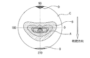
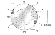
次に、上記実施例1、及び比較サンプル1の液晶表示装置について、反射表示のコントラストの視角特性を評価した。その結果を図5及び図6に示す。また、実施例1の液晶表示装置について透過表示のコントラストの視角特性の測定結果を図7に示す。また、比較サンプル2,3の液晶表示装置について反射表示におけるコントラストの視角特性の測定結果を図8及び図9に示す。
【0059】
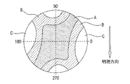
図5ないし図9において、中心が表示装置の正面に対応しており、中心から離れるに従って視角が大きくなっている。また、符号Aで示された領域(図中左上がりの鎖線で示す領域)は、測定範囲内におけるコントラストの最大値の75%以上のコントラストが得られた視角範囲を示し、符号Bで示された領域(図中右上がりの鎖線で示す領域)は、同、50%以上のコントラストが得られた視角範囲を示し、符号Cで示された領域(図中模様無しの領域)は、同、50%未満のコントラストが得られた視角範囲を示している。また、図6中、符号Dで示された領域(図中水平線で示す領域)は、コントラストが1未満となった領域であり、すなわち表示が反転して視認された視角範囲である。
【0060】
図5に示すように、本発明の構成要件を満たす実施例1の液晶表示装置では、より広い視角範囲が得られ、また液晶表示装置の正面を中心として左右対称に高コントラストの領域(領域A)が分布している。これに対して、図6に示す比較サンプル1の液晶表示装置では、最大コントラストの50%以上が得られる視角範囲が図5に比して狭く、また、高コントラスト領域(領域A)も、左右対称になっていない。また、図6中左右端に、表示が反転した領域Dが現れており、この点においても図5に示す実施例1の液晶表示装置の方が視角が広いことが分かる。
【0061】
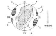
また、図8及び図9に示す、位相差層の配向方向が3時方向、及び9時方向とされた液晶表示装置では、高コントラスト領域(領域A)が、高視角側に現れており、通常観察者から視認される液晶表示装置正面方向ではコントラストがやや低くなる。そのため、実質的にコントラストの低下が生じている。また、図8及び図9のいずれにおいても、表示が反転した領域Dが現れており、視角がやや狭くなっている。
【0062】
本実施形態の液晶表示装置では、図7に示す透過表示でも、高コントラストの領域が左右対称に分布しているので、透過表示、反射表示のいずれにおいても、左右対称な表示特性を有しており、実質的に視認性の高い表示を実現している。
このように、本発明の要件を満たす実施例1の液晶表示装置によれば、視角が広く、かつ左右対称にコントラストが分布した視認性に優れる反射表示及び透過表示が得られる。
【0063】
(実施例2)
次に、実施例2として、上記実施例1と位相差層の構成のみを異ならせた液晶表示装置を作製した。つまり、パネルの構成として、画素数を160×120、画素ピッチを255μm、透過表示領域となる開口部の面積を68μm×22μm(ただし、この開口部を1ドットに2個形成)、とした。
液晶層16は右90°ツイストのTN液晶とし、6時明視(表示装置正面の観察者から見て手前側方向が明視方向)とした。反射表示領域の液晶層のリタデーション(Δn・d)は0.26、透過表示領域の液晶層のリタデーションは0.48とした。位相差層20は、上記実施の形態で説明した第1の形成方法(高分子液晶を用いる方法)に準じて形成し、その配向方向を12時方向(表示装置正面の観察者から見て奥側方向)とした。位相差層を構成する高分子液晶はスプレイ構造とし、その仰角(図4(b)に示す角度α、β)は位相差層内で連続的に変化するようにし、仰角の最小値βを3°、最大値αを50°とした。位相差層20は正面方向のリタデーションが1/4波長となるようにした。
【0064】
次いで、比較サンプル4として、上記実施例2の構成において、位相差層20の高分子液晶の配向方向を6時方向(表示装置正面の観察者から見て手前側方向)とした以外は同様の構成を備えた液晶表示装置を作製した。
次に、比較サンプル5として、上記実施例2の構成において、位相差層20の高分子液晶の配向方向を3時方向(表示装置正面の観察者から見て手前側方向)とした以外は同様の構成を備えた液晶表示装置を作製した。
次に、比較サンプル6として、上記実施例1の構成において、位相差層20の高分子液晶の配向方向を9時方向(表示装置正面の観察者から見て手前側方向)とした以外は同様の構成を備えた液晶表示装置を作製した。
【0065】
次に、上記実施例2、及び比較サンプル4〜6の液晶表示装置について、反射表示のコントラストの視角特性を評価した。その結果を図10ないし及び図13に示す。これらの図に示すA〜Dの領域の定義については上記実施例1と同様である。
【0066】
図10に示すように、本発明の構成要件を満たす実施例2の液晶表示装置では、より広い視角範囲が得られ、また液晶表示装置の正面を中心として左右対称に高コントラストの領域(領域A)が分布している。これに対して、図11に示す比較サンプル4の液晶表示装置では、最大コントラストの50%以上が得られる視角範囲が図10に比して狭く、また、高コントラスト領域(領域A)も、左右対称になっていない。また、図11中左右端に、表示が反転した領域Dが現れており、この点においても図10に示す実施例2の液晶表示装置の方が視角が広いことが分かる。
また、実施例2の液晶表示装置では、透過表示領域の構成は上記実施例1と同様としているため、透過表示の視角特性としては図7に示すものと極めて近いものが得られると考えられる。従って、本例の液晶表示装置においても、透過表示、反射表示のいずれにおいても左右対称のコントラストの分布が得られ、視認性に優れる表示が得られる。
【0067】
また、位相差層の高分子液晶の配向方向が、3時方向及び9時方向とされた比較サンプル5,6は、図12及び図13に示すように、いずれも高コントラスト領域Aが図中心から外れており、実質的なコントラストの低下が生じていることが分かる。また、いずれのサンプルにおいても、表示が反転した領域Dが現れており、この点においても視角が狭くなっている。
このように、本発明の要件を満たす実施例2の液晶表示装置によれば、位相差層を構成する高分子液晶がスプレイ構造を成して配向されていても、視角が広く、かつ左右対称にコントラストが分布した視認性に優れる反射表示及び透過表示が得られることが分かる。
【図面の簡単な説明】
【図1】図1は、本発明の第1の実施形態の液晶表示装置の概略構成を示す断面図である。
【図2】図2は、図1に示す液晶層と位相差層を構成する液晶分子の配向状態の説明図であり、図2(a)は模式断面構造、図2(b)は模式平面構造を示している。
【図3】図3は、同、液晶表示装置の表示原理を説明するための図であって、表示原理の説明に必要な構成要素のみを示す図である。
【図4】図4は、図1に示す位相差層の高分子液晶の配向構造を示す図であり、図4(a)はチルト構造、図4(b)はスプレイ構造を示している。
【図5】図5は、実施例における視角特性の評価結果を示す図である。
【図6】図6は、実施例における視角特性の評価結果を示す図である。
【図7】図7は、実施例における視角特性の評価結果を示す図である。
【図8】図8は、実施例における視角特性の評価結果を示す図である。
【図9】図9は、実施例における視角特性の評価結果を示す図である。
【図10】図10は、実施例における視角特性の評価結果を示す図である。
【図11】図11は、実施例における視角特性の評価結果を示す図である。
【図12】図12は、実施例における視角特性の評価結果を示す図である。
【図13】図13は、実施例における視角特性の評価結果を示す図である。
【図14】図14は、本発明の液晶表示装置における反射表示領域のΔn・dと反射率との相関関係を示すシミュレーション結果である。
【図15】図15は、従来の半透過反射型液晶表示装置の部分断面図である。
【図16】図16は、本発明に係る電子機器の一例を示す斜視図である。
【符号の説明】
10 液晶表示装置、11 液晶セル、12 バックライト、13 下基板、14 上基板、16 液晶層、16a 液晶分子、18 半透過反射層、18a開口部、20 位相差層、20a 高分子液晶(液晶性化合物)、20d ダイレクタ、21 保護層、28 下偏光板、36 上偏光板、R 反射表示領域、T 透過表示領域[0001]
TECHNICAL FIELD OF THE INVENTION
The present invention relates to a liquid crystal display device and an electronic device, and in particular, to a transflective liquid crystal display device, and particularly to a transflective liquid crystal display device, which has an excellent visibility capable of performing a sufficiently bright display not only in the reflection mode but also in the transmission mode. And a liquid crystal display device having the same.
[0002]
[Prior art]
2. Description of the Related Art Conventionally, there has been proposed a liquid crystal display device that uses external light in a bright place as in a normal reflection type liquid crystal display device, and makes a display visible by an internal light source in a dark place. This liquid crystal display device employs a display system having both a reflective type and a transmissive type, and reduces power consumption by switching to either a reflective display or a transmissive display according to the surrounding brightness. Even when the surroundings are dark, clear display can be performed.
[0003]
FIG. 15 is a cross-sectional structural view showing an example of a transflective liquid crystal display device using such a transflective film, and has a configuration described in Patent Document 1 filed by the present applicant. It is.
In this liquid
[0004]
According to the liquid
[0005]
On the other hand, in the configuration described in Patent Literature 2 in which the circularly polarizing layer is provided on the inner surface side of the liquid crystal panel, it is possible to increase the use efficiency of the backlight light. This circularly polarizing layer is an optical layer having a property of transmitting circularly polarized light in a specific rotation direction and reflecting circularly polarized light in the opposite direction. The light reflected by the circularly polarizing layer is returned to the backlight side and re-transmitted. It is designed to be used. Further, the document discloses a configuration in which a retardation layer made of a liquid crystalline compound is provided on the liquid crystal layer side of the circularly polarizing layer, and light transmitted through the circularly polarizing layer is converted into linearly polarized light to perform display using linearly polarized light. It has been disclosed.
[0006]
[Patent Document 1]
Japanese Patent No. 3235102
[Patent Document 2]
JP-A-9-258210
[0007]
[Problems to be solved by the invention]
It is considered that if the technology described in Patent Document 2 is applied to the liquid crystal display device described in Patent Document 1, the efficiency of use of backlight light can be improved, and the brightness of display can be improved. However, such an effect can be obtained only in the transmissive display area of the transflective liquid crystal display device. Further, Patent Document 2 does not disclose application to a reflective or transflective liquid crystal display device.
[0008]
The present invention has been made in view of the above circumstances, and is a reflective or semi-transmissive display having improved display brightness, improved viewing angle, and improved backlight utilization efficiency. It is an object of the present invention to provide a reflective liquid crystal display device.
[0009]
[Means for Solving the Problems]
The present invention provides a liquid crystal display device and an electronic device having the following configurations to achieve the above object.
In a liquid crystal display device according to the present invention, in a liquid crystal display device in which a TN mode liquid crystal layer is sandwiched between an upper substrate and a lower substrate that are arranged to face each other, an upper polarizing plate is provided on the upper substrate side of the liquid crystal layer. Provided on the inner surface side of the lower substrate, a reflection layer and a retardation layer mainly composed of a liquid crystal compound oriented with a finite tilt angle in order from the substrate side, and the retardation layer is provided. It is characterized in that the director of the liquid crystal compound constituting the layer is oriented substantially parallel and substantially opposite to the clear viewing direction of the liquid crystal display device in plan view.
[0010]
The liquid crystal display device according to the present invention includes a retardation layer on a liquid crystal layer side of a reflective layer for performing a reflective display, and a director of a liquid crystal compound constituting the retardation layer is a light-emitting device of the liquid crystal display device. By being arranged so as to have the above-mentioned azimuthal relationship with respect to the viewing direction, the viewing angle characteristics in the reflection display are improved, and a high-contrast display can be obtained with a wide viewing angle. The present inventor has verified that the orientation direction of the polymer liquid crystal in the retardation layer is appropriate using a prototype liquid crystal display device, and details thereof are described in (Examples). I have.
In addition, the direction of the director of the liquid crystal compound refers to the direction of a vector indicating the direction rising from the horizontal plane toward the upper substrate along the longitudinal direction of the liquid crystal compound, similarly to the director of the liquid crystal molecules forming the liquid crystal layer. . In the TN mode liquid crystal layer, the clear viewing direction is the direction of the director of the liquid crystal molecules arranged substantially at the center in the layer thickness direction.
[0011]
Next, in the liquid crystal display device of the present invention, a TN mode liquid crystal layer is sandwiched between an upper substrate and a lower substrate which are arranged to face each other, and a transmissive display region and a reflective display region are formed in one dot region. In the transflective liquid crystal display device having an upper polarizing plate provided on the upper substrate side of the liquid crystal layer, a reflective layer in order from the substrate side in the reflective display area on the inner surface side of the lower substrate, a finite tilt angle And a retardation layer mainly composed of a liquid crystal compound that is aligned and has a director. The director of the liquid crystal compound constituting the retardation layer is substantially the same as the clear viewing direction of the liquid crystal display device in plan view. The liquid crystal layer is oriented in parallel and substantially in the opposite direction, and the phase difference of the liquid crystal layer in the transmissive display region is increased when the selection voltage is applied or the non-selection voltage is applied. Greater than And it features.
[0012]
The above configuration is obtained by applying the configuration of the reflective liquid crystal display device to a transflective liquid crystal display device, and in the reflective display region, a retardation layer is provided on the reflective layer. The director of the high-molecular liquid crystal constituting the liquid crystal display device is substantially parallel to the clear viewing direction of the liquid crystal display device in plan view and substantially in the opposite direction. According to the liquid crystal display device having such a configuration, it is possible to obtain a high contrast display in a wide viewing angle range in a reflective display, and to solve the problem that the luminance of the transmissive display of the conventional transflective liquid crystal display device is insufficient. It is.
[0013]
That is, in the above configuration, the retardation layer is provided only in the reflective display area on the inner surface of the lower substrate, and in the transmissive display area, the phase difference is added only to the reflective display area due to the presence of the retardation layer. Of the liquid crystal layer in the reflective display area is larger than that in the reflective display area. In this configuration, it is possible to display only linearly polarized light in the transmissive display depending on the setting conditions such as the phase difference of the retardation layer and the liquid crystal layer, and not only the lower retardation plate but also the upper retardation plate can be displayed. It can be unnecessary. As a result, it is possible to solve the problem that the transmission display is darkened by absorbing approximately half of the circularly polarized light by the upper polarizer in the conventional configuration, and it is possible to make the transmission display brighter than in the related art. Further, the structure is simpler than that of the related art, and the thickness of the device can be reduced. The display principle of the liquid crystal display device of the present invention will be described in (Embodiments of the invention).
[0014]
In the liquid crystal display device of the present invention, the liquid crystal compound forming the retardation layer is oriented in a tilt structure, and the average tilt angle of the liquid crystal compound is 2 ° or more and 35 ° or less. Is preferred. When the average tilt angle is less than 2 °, the effect of improving the viewing angle is hardly obtained. At a tilt angle exceeding 35 °, the viewing angle characteristics deteriorate. Specifically, the contrast is not maximized in front of the liquid crystal display device, but is maximized when viewed from an oblique direction, so that the substantial contrast visually recognized by an observer is reduced. If the tilt angle exceeds 35 °, the driving voltage tends to increase, which is not preferable in terms of power consumption.
[0015]
In the liquid crystal display device according to the aspect of the invention, it is preferable that an average tilt angle of the liquid crystal compound forming the retardation layer is 10 ° or more and 25 ° or less.
With such a configuration, it is possible to obtain a liquid crystal display device having a viewing angle characteristic symmetrical in the left-right direction of the viewer in front of the liquid crystal display device, and particularly excellent in visibility.
[0016]
Further, in the liquid crystal display device of the present invention, the liquid crystal compound forming the retardation layer may be configured to have a spray structure and be oriented.
Even with the above configuration, the liquid crystal display device of the present invention can provide a bright display with a wide viewing angle.
[0017]
In the liquid crystal display device of the present invention, it is preferable that a liquid crystal layer thickness in the transmissive display area is larger than a liquid crystal layer thickness in the reflective display area. With such a configuration, the birefringence effect on light transmitted through the liquid crystal layer can be made closer between the transmissive display region and the reflective display region, and display contrast can be improved.
[0018]
In the liquid crystal display device according to the aspect of the invention, it is preferable that the liquid crystal layer thickness in the transmissive display region is approximately twice the liquid crystal layer thickness in the reflective display region.
That is, as means for making the phase difference of the liquid crystal layer in the transmissive display area larger than the phase difference of the liquid crystal layer in the reflective display area, for example, the thickness of the liquid crystal layer is d, and the refractive index anisotropy of the liquid crystal is Δn. Then, since the birefringence phase difference (retardation) is represented by the product Δn · d, at least one of the thickness d of the liquid crystal layer and the refractive index anisotropy Δn of the liquid crystal is reflected between the transmissive display region and the reflective region. What is necessary is just to make it different from the display area. However, in practice, it is difficult to greatly change the refractive index anisotropy Δn of the liquid crystal in the transmissive display area and the reflective display area. Therefore, the thickness of the liquid crystal layer in the transmissive display area is larger than the thickness of the liquid crystal layer in the reflective display area. It is easy to set large.
The above configuration is a liquid crystal display device having a so-called multi-gap structure. By introducing the configuration according to the liquid crystal display device of the present invention, the substantial retardation of the liquid crystal layer in the transmissive display region and the substantial retardation of the reflective display region are achieved. Can be easily prepared, and a high-contrast liquid crystal display device can be realized.
[0019]
In the liquid crystal display device of the present invention, it is preferable that Δnd of the liquid crystal layer in the reflective display region is 0.13 or more and 0.34 or less. With the above range, a reflective display with high brightness and high contrast can be obtained. If it exceeds the above range, the brightness and contrast tend to decrease, which is not preferable.
[0020]
In the liquid crystal display device of the present invention, it is preferable that the retardation layer imparts a birefringent retardation of approximately 波長 wavelength to transmitted light.
With the above configuration, for example, when the retardation of the liquid crystal layer in the transmissive display area is set to 波長 wavelength and the retardation of the reflective display area is set to 4 wavelength, the transmission of the upper polarizer between the reflective display and the transmissive display is performed. The polarization state at the time can be aligned with linearly polarized light in substantially the same direction, and the retardation in the reflective display area and the retardation in the transmissive display area can be made substantially equal, so that the light use efficiency can be improved most and the transmissive display is the brightest. It can be configured. Further, a display with high contrast can be obtained.
[0021]
Next, an electronic apparatus of the present invention includes the above-described liquid crystal display device of the present invention. According to such a configuration, it is possible to provide an electronic device including a display unit capable of obtaining a high-brightness, high-contrast display in any of the transmissive display and the reflective display and obtaining a reflective display with a wide viewing angle.
[0022]
BEST MODE FOR CARRYING OUT THE INVENTION
Hereinafter, embodiments of the present invention will be described with reference to the drawings.
FIG. 1 is a cross-sectional view showing a schematic configuration of a liquid crystal display device according to the present embodiment, and FIG. 2 is a diagram for explaining a display principle thereof, showing only constituent elements necessary for explaining the display principle. It is. This embodiment is an example of an active matrix type transflective color liquid crystal display device. In all of the following drawings, the thickness of each component, the ratio of dimensions, and the like are appropriately changed in order to make the drawings easy to see.
[0023]
As shown in FIG. 1, a liquid
[0024]
On the inner surface side of the
[0025]
On the
[0026]
These
In the first method, first, SE-3140 (trade name, manufactured by Nissan Chemical Industries, Ltd.) as an alignment film material is spin-coated or flexo-printed on a substrate on which the
[0027]
Next, the polymer liquid crystal layer is prebaked at 80 ° C. for 1 minute, further heated at 180 ° C., which is higher than the isotropic transition temperature (170 ° C.) of the polymer liquid crystal, for 30 minutes, and gradually cooled to be cooled. Is oriented. When the present inventors actually manufactured the device under these conditions, a film thickness of 630 nm and a phase difference of 133 nm were obtained.
[0028]
Next, an acrylic photosensitive resin NN-525 (trade name, manufactured by JSR Corporation) is applied as a material for the protective layer by a spin coating method (for example, at a rotation speed of 700 rpm for 30 seconds). At this time, the film thickness was 2.3 μm. Next, after prebaking the protective layer at 80 ° C. for 3 minutes, exposure using a photomask (for example, when the exposure intensity is 140 mJ / cm) 2 , A value measured with an ultraviolet light meter having a sensitivity of 350 nm), immersed in an alkaline developer at room temperature for 90 seconds to perform development, and the protective layer is left only in the reflective display area. Since the acrylic photosensitive resin is negative type, it is necessary to form a photomask so that the reflective display area is exposed.
[0029]
Next, in order to completely cure the protective layer, post-exposure was performed at an exposure intensity of 2000 mJ / cm. 2 Do with. In addition, 1000 mJ / cm 2 In the following, peeling of the protective layer occurred during the development of the polymer liquid crystal in the next step, but 1300 mJ / cm 2 Since there was no problem with the above, 2000 mJ / cm 2 Was set. Next, the polymer liquid crystal is etched by immersion in an etchant composed of N-methyl-2-pyrrolidinone at room temperature for 30 minutes. Next, the substrate is dried at 80 ° C. for 3 minutes to form a
[0030]
In the second method, a UV curable liquid crystal UCL-008-K1 (trade name, manufactured by Dainippon Ink and Chemicals, Inc.) is formed on a substrate on which an alignment film is formed in the same manner as in the first method. Is applied by a spin coating method (for example, at a rotation speed of 700 rpm for 30 seconds). The liquid crystalline monomer solution used here was diluted to 25% in a mixed solvent of N-methyl-2-pyrrolidinone and γ-butyrolactone, and had an isotropic transition temperature of 69 ° C. and a refractive index anisotropy Δn of 0.20. is there.
[0031]
Next, the liquid crystalline monomer is dried at 60 ° C. for 5 minutes, heated at 90 ° C. which is higher than the isotropic transition temperature (69 ° C.) for 5 minutes, and then gradually cooled to align the liquid crystalline monomer. When the present inventors actually manufactured under these conditions, a film thickness of 650 nm was obtained. Next, exposure using a photomask (for example, an exposure intensity of 3000 mJ / cm 2 ) To locally photopolymerize the liquid crystalline monomer, and then immerse in an alkaline developer or a ketone-based organic solvent for 60 seconds for development, leaving the liquid crystalline monomer polymer only in the reflective display area. Let it. Thereby, the
[0032]
As described above, in the liquid
[0033]
On the other hand, a common electrode 32 made of a transparent conductive film such as ITO and an
[0034]
The
[0035]
The
[0036]
In the liquid crystal display device of the present embodiment having the above configuration, the azimuth relationship between the director of the liquid crystal compound of the
[0037]
FIG. 2A is a cross-sectional configuration diagram illustrating the
FIGS. 2A and 2B show a state where a non-selection voltage is applied to the
[0038]
As shown in FIGS. 2A and 2B, the clear viewing direction of the liquid crystal display device of the present embodiment is determined by the direction of the
[0039]
Arrows indicated by
[0040]
In the liquid crystal display device of the present embodiment, the
[0041]
In the case of the present embodiment, the
[0042]
FIG. 4A is a schematic diagram illustrating liquid crystal molecules aligned in a tilt structure, and FIG. 4B is a schematic diagram illustrating liquid crystal molecules aligned in a splay structure. is there. The arrows shown in these figures correspond to the thickness direction of the
As described above, in the present embodiment, the
[0043]
Further, in the present embodiment, the case where the
In the spray structure shown in FIG. 4B, the angles α and β represent the maximum value α and the minimum value β of the elevation angle of the
[0044]
Next, the display principle of the liquid
First, when performing a dark display, a state where a voltage is applied to the liquid crystal layer 16 (selection voltage applied state) is set so that the retardation in the
[0045]
On the other hand, in the transmissive display, when the transmission axis of the lower
[0046]
Next, when performing bright display, a state in which no voltage is applied to the liquid crystal layer 16 (a state in which a non-selection voltage is applied) is set, the retardation in the reflective display region R is 波長 wavelength, and the retardation in the transmissive display region T is 1/1. The wavelength is set to 2 wavelengths. In the reflective display, the linearly polarized light perpendicular to the paper surface transmitted through the upper
[0047]
On the other hand, in the transmissive display, the linearly polarized light parallel to the paper surface emitted from the
In transmissive display, of the linearly polarized light transmitted through the lower
[0048]
In the liquid
[0049]
According to this configuration, in the conventional configuration, almost half of the circularly polarized light incident from the liquid crystal layer side is absorbed by the upper polarizer, so that the transmissive display becomes dark, and illumination reflected on the back surface of the semi-transmissive reflective layer. Since both of the problems that light is absorbed by the lower polarizing plate and cannot be reused for display can be solved at the same time, the transmissive display can be made brighter than before. In the case of the present embodiment, in particular, the retardation in the transmissive display region T is twice as large as that in the reflective display region R, so that the polarization state before transmission through the upper
[0050]
According to the configuration of the present embodiment, although the
[0051]
The inventor obtained a simulation of a correlation between the phase difference (retardation R = Δn · d) of the reflective display region and the reflectance in the liquid crystal display device of the present embodiment. FIG. 14 shows the simulation results. The horizontal axis in FIG. 14 is Δn · d [nm], and the vertical axis is reflectance [−]. In the case of the present embodiment, since the transmissive display is a TN mode display, the light use efficiency is high and a bright display is obtained. On the other hand, the reflective display has a practically necessary brightness of at least a reflectance of 20% or more. Is required. In order to obtain this level of reflectance, the phase difference (Δnd) of the reflective display region needs to be in the range of 130 nm ≦ Δnd ≦ 340 nm. By setting Δn · d of the reflective display area so as to satisfy this condition, visibility of the reflective display can be ensured.
[0052]
The technical scope of the present invention is not limited to the above-described embodiment, and various changes can be made without departing from the spirit of the present invention. For example, in the above embodiment, the retardation in the retardation layer on the reflective display area is set to 波長 wavelength, and the thickness of the liquid crystal layer in the transmissive display area is set to twice the thickness of the reflective display area. The retardation of the liquid crystal layer was almost 0 in both the reflective display area and the transmissive display area, and the retardation of the liquid crystal layer when a non-selective voltage was applied was 波長 wavelength in the reflective display area and 波長 wavelength in the transmissive display area. Although this setting makes the transmissive display the brightest and improves the contrast the most, the retardation of each part does not necessarily have to be the same as the above setting, and the retardation by the
[0053]
In the above embodiment, the positive type liquid crystal is used, the initial state is horizontal alignment, the retardation at the time of voltage application is almost 0, the retardation of the reflective display area is 波長 wavelength when no voltage is applied, and the retardation of the transmissive display area is 1 In contrast to this, a negative type liquid crystal is used, the initial state is vertical alignment, the phase shift is almost 0 when no voltage is applied, and the retardation of the reflective display area is 1 when voltage is applied. It is also possible to configure so that the retardation of the 表示 wavelength and the transmissive display area is 波長 wavelength. Further, the present invention is not limited to the active matrix type transflective color liquid crystal display device as in the above embodiment, but can be applied to a passive matrix type monochrome liquid crystal display device.
[0054]
(Electronics)
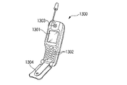
FIG. 16 is a perspective view of a mobile phone which is an example of an electronic apparatus including a liquid crystal display device according to the present invention in a display portion. 1301, a plurality of
The liquid crystal display device of the above embodiment is not limited to the above-mentioned mobile phone, but may be an electronic book, a personal computer, a digital still camera, a liquid crystal television, a viewfinder type or a monitor direct view type video tape recorder, a car navigation device, a pager, and an electronic organizer. , A calculator, a word processor, a workstation, a videophone, a POS terminal, a device equipped with a touch panel, etc., and can be suitably used as an image display means. And a bright display with a wide viewing angle.
[0055]
【Example】
Hereinafter, the liquid crystal display device of the present invention will be described in more detail with reference to examples. In this example, in the liquid crystal display device having the structure of the above-described embodiment, a liquid crystal display device having a retardation layer made of a liquid crystal compound with different alignment directions was manufactured, and the viewing angle characteristics were evaluated. The results are reported below.
[0056]
(Example 1)
As the liquid crystal display device of Example 1, the liquid crystal display device having the configuration of the above embodiment shown in FIG. 1 was manufactured. The configuration of the panel was such that the number of pixels was 160 × 120, the pixel pitch was 255 μm, and the area of an opening serving as a transmissive display area was 68 μm × 22 μm (however, two such openings were formed in one dot).
The
[0057]
Next, as Comparative Sample 1, the same configuration as in Example 1 was used except that the alignment direction of the polymer liquid crystal of the
Next, the same as Comparative Sample 2 except that the alignment direction of the polymer liquid crystal of the
Next, the same as Comparative Sample 3 except that the alignment direction of the polymer liquid crystal of the
[0058]
Next, with respect to the liquid crystal display devices of Example 1 and Comparative Sample 1, the viewing angle characteristics of the contrast of the reflective display were evaluated. The results are shown in FIGS. FIG. 7 shows the measurement results of the viewing angle characteristics of the contrast of the transmissive display for the liquid crystal display device of Example 1. 8 and 9 show the measurement results of the viewing angle characteristics of the contrast in reflective display for the liquid crystal display devices of Comparative Samples 2 and 3. FIG.
[0059]
5 to 9, the center corresponds to the front of the display device, and the viewing angle increases as the distance from the center increases. A region indicated by reference sign A (a region indicated by a chain line rising to the left in the figure) indicates a viewing angle range in which a contrast of 75% or more of the maximum value of the contrast within the measurement range is obtained, and is indicated by reference sign B. A region (region indicated by a chain line rising to the right in the figure) indicates a viewing angle range in which a contrast of 50% or more was obtained, and a region indicated by reference numeral C (region without a pattern in the diagram) indicates the same. This shows a viewing angle range where a contrast of less than 50% is obtained. In FIG. 6, a region indicated by a reference symbol D (a region indicated by a horizontal line in the drawing) is a region where the contrast is less than 1, that is, a viewing angle range in which the display is inverted and visually recognized.
[0060]
As shown in FIG. 5, in the liquid crystal display device of Example 1 that satisfies the constitutional requirements of the present invention, a wider viewing angle range can be obtained, and a high contrast region (region A) is symmetrical with respect to the front of the liquid crystal display device. ) Are distributed. On the other hand, in the liquid crystal display device of Comparative Sample 1 shown in FIG. 6, the viewing angle range in which 50% or more of the maximum contrast can be obtained is narrower than that in FIG. 5, and the high contrast region (region A) is also left and right. Not symmetric. In addition, a region D in which the display is inverted appears at the left and right ends in FIG. 6, and it can be seen that the viewing angle of the liquid crystal display device of Example 1 shown in FIG.
[0061]
In the liquid crystal display device shown in FIGS. 8 and 9 in which the orientation direction of the retardation layer is set to the 3 o'clock direction and the 9 o'clock direction, a high contrast region (region A) appears on the high viewing angle side. The contrast is slightly lower in the front direction of the liquid crystal display device which is usually visually recognized by a viewer. Therefore, the contrast is substantially reduced. Further, in both FIG. 8 and FIG. 9, a region D whose display is inverted appears, and the viewing angle is slightly narrowed.
[0062]
In the liquid crystal display device of the present embodiment, even in the transmissive display shown in FIG. 7, since the high contrast regions are symmetrically distributed, the transmissive display and the reflective display have symmetric display characteristics. Thus, a display with substantially high visibility is realized.
As described above, according to the liquid crystal display device of the first embodiment that satisfies the requirements of the present invention, it is possible to obtain a reflective display and a transmissive display having a wide viewing angle and excellent contrast in which the contrast is symmetrically distributed.
[0063]
(Example 2)
Next, as Example 2, a liquid crystal display device in which only the configuration of the retardation layer was different from that of Example 1 was manufactured. That is, the configuration of the panel was such that the number of pixels was 160 × 120, the pixel pitch was 255 μm, and the area of the opening serving as the transmissive display area was 68 μm × 22 μm (however, two such openings were formed in one dot).
The
[0064]
Next, as Comparative Sample 4, the same configuration as that of Example 2 was performed except that the alignment direction of the polymer liquid crystal of the
Next, Comparative Sample 5 was the same as Example 2 except that the alignment direction of the polymer liquid crystal of the
Next, Comparative Sample 6 was the same as in Comparative Example 6, except that the alignment direction of the polymer liquid crystal of the
[0065]
Next, with respect to the liquid crystal display devices of Example 2 and Comparative Samples 4 to 6, the viewing angle characteristics of the contrast of the reflective display were evaluated. The results are shown in FIGS. 10 to 13. The definitions of the areas A to D shown in these figures are the same as in the first embodiment.
[0066]
As shown in FIG. 10, in the liquid crystal display device according to the second embodiment that satisfies the configuration requirements of the present invention, a wider viewing angle range can be obtained, and a high contrast region (region A) is symmetrical with respect to the front of the liquid crystal display device. ) Are distributed. On the other hand, in the liquid crystal display device of Comparative Sample 4 shown in FIG. 11, the viewing angle range in which 50% or more of the maximum contrast can be obtained is narrower than that in FIG. 10, and the high contrast region (region A) is also left and right. Not symmetric. In addition, a region D where the display is inverted appears at the left and right ends in FIG. 11, and it can be seen that the viewing angle of the liquid crystal display device of Example 2 shown in FIG.
Further, in the liquid crystal display device of the second embodiment, since the configuration of the transmissive display area is the same as that of the first embodiment, it is considered that the viewing angle characteristic of the transmissive display is very close to that shown in FIG. Therefore, also in the liquid crystal display device of this example, a symmetric contrast distribution is obtained in both the transmissive display and the reflective display, and a display with excellent visibility is obtained.
[0067]
In Comparative Samples 5 and 6, in which the orientation directions of the polymer liquid crystal in the retardation layer were set to the 3 o'clock direction and the 9 o'clock direction, as shown in FIGS. It can be seen that the contrast is substantially lowered. In addition, in each of the samples, a region D whose display is inverted appears, and also at this point, the viewing angle is narrow.
As described above, according to the liquid crystal display device of Example 2 which satisfies the requirements of the present invention, even when the polymer liquid crystal constituting the retardation layer is oriented in a splay structure, the viewing angle is wide and the symmetry is left-right. It can be seen that a reflective display and a transmissive display having excellent visibility with contrast distributed can be obtained.
[Brief description of the drawings]
FIG. 1 is a cross-sectional view illustrating a schematic configuration of a liquid crystal display device according to a first embodiment of the present invention.
FIG. 2 is an explanatory view of an alignment state of liquid crystal molecules constituting a liquid crystal layer and a retardation layer shown in FIG. 1; FIG. 2 (a) is a schematic sectional structure, and FIG. 2 (b) is a schematic plane; Shows the structure.
FIG. 3 is a diagram for explaining the display principle of the liquid crystal display device, showing only components necessary for explaining the display principle.
FIG. 4 is a view showing an alignment structure of a polymer liquid crystal in a retardation layer shown in FIG. 1, wherein FIG. 4 (a) shows a tilt structure and FIG. 4 (b) shows a spray structure.
FIG. 5 is a diagram illustrating evaluation results of viewing angle characteristics in an example.
FIG. 6 is a diagram illustrating evaluation results of viewing angle characteristics in an example.
FIG. 7 is a diagram illustrating evaluation results of viewing angle characteristics in an example.
FIG. 8 is a diagram illustrating evaluation results of viewing angle characteristics in the example.
FIG. 9 is a diagram illustrating evaluation results of viewing angle characteristics in the example.
FIG. 10 is a diagram illustrating evaluation results of viewing angle characteristics in an example.
FIG. 11 is a diagram illustrating evaluation results of viewing angle characteristics in the example.
FIG. 12 is a diagram illustrating evaluation results of viewing angle characteristics in an example.
FIG. 13 is a diagram illustrating evaluation results of viewing angle characteristics in the example.
FIG. 14 is a simulation result showing a correlation between Δn · d of a reflective display area and a reflectance in the liquid crystal display device of the present invention.
FIG. 15 is a partial cross-sectional view of a conventional transflective liquid crystal display device.
FIG. 16 is a perspective view illustrating an example of an electronic apparatus according to the invention.
[Explanation of symbols]
Claims (10)
前記液晶層の上基板側に上偏光板が設けられ、前記下基板の内面側に、基板側から順に反射層と、有限のチルト角を有して配向された液晶性化合物を主体とする位相差層とが設けられており、
前記位相差層を構成する液晶性化合物のダイレクタが、平面視において当該液晶表示装置の明視方向と略平行かつ略逆向きに配向されていることを特徴とする液晶表示装置。In a liquid crystal display device in which a TN mode liquid crystal layer is sandwiched between an upper substrate and a lower substrate which are arranged to face each other,
An upper polarizer is provided on the upper substrate side of the liquid crystal layer, and a reflective layer and a liquid crystal compound mainly aligned with a finite tilt angle are arranged on the inner surface side of the lower substrate in this order from the substrate side. A phase difference layer is provided,
A liquid crystal display device wherein the director of the liquid crystal compound constituting the retardation layer is oriented substantially parallel to and substantially opposite to the clear viewing direction of the liquid crystal display device in plan view.
前記液晶層の上基板側に上偏光板が設けられ、前記下基板の内面側の前記反射表示領域に基板側から順に反射層と、有限のチルト角を有して配向された液晶性化合物を主体とする位相差層とが設けられており、
前記位相差層を構成する液晶性化合物のダイレクタが、平面視において当該液晶表示装置の明視方向と略平行かつ略逆向きに配向されており、
選択電圧印加時、非選択電圧印加時のいずれか一方において、前記透過表示領域における前記液晶層の位相差が前記反射表示領域における前記液晶層の位相差よりも大きいことを特徴とする液晶表示装置。A transflective liquid crystal display device in which a TN mode liquid crystal layer is sandwiched between an upper substrate and a lower substrate which are arranged to face each other and has a transmissive display region and a reflective display region within one dot region,
An upper polarizing plate is provided on the upper substrate side of the liquid crystal layer, and a reflective layer and a liquid crystal compound aligned with a finite tilt angle in order from the substrate side in the reflective display area on the inner surface side of the lower substrate. A phase difference layer as a main component is provided,
The director of the liquid crystalline compound constituting the retardation layer is oriented in a direction substantially parallel and substantially opposite to the clear viewing direction of the liquid crystal display device in plan view,
A liquid crystal display device, wherein a phase difference of the liquid crystal layer in the transmissive display area is larger than a phase difference of the liquid crystal layer in the reflective display area, when either a selection voltage is applied or a non-selection voltage is applied. .
Priority Applications (1)
| Application Number | Priority Date | Filing Date | Title |
|---|---|---|---|
| JP2003016219A JP2004226830A (en) | 2003-01-24 | 2003-01-24 | Liquid crystal display and electronic equipment |
Applications Claiming Priority (1)
| Application Number | Priority Date | Filing Date | Title |
|---|---|---|---|
| JP2003016219A JP2004226830A (en) | 2003-01-24 | 2003-01-24 | Liquid crystal display and electronic equipment |
Publications (1)
| Publication Number | Publication Date |
|---|---|
| JP2004226830A true JP2004226830A (en) | 2004-08-12 |
Family
ID=32903748
Family Applications (1)
| Application Number | Title | Priority Date | Filing Date |
|---|---|---|---|
| JP2003016219A Pending JP2004226830A (en) | 2003-01-24 | 2003-01-24 | Liquid crystal display and electronic equipment |
Country Status (1)
| Country | Link |
|---|---|
| JP (1) | JP2004226830A (en) |
Cited By (5)
| Publication number | Priority date | Publication date | Assignee | Title |
|---|---|---|---|---|
| JP2007241037A (en) * | 2006-03-10 | 2007-09-20 | Toppan Printing Co Ltd | Polarizing element, manufacturing method thereof, and liquid crystal display element |
| JP2008209553A (en) * | 2007-02-26 | 2008-09-11 | Epson Imaging Devices Corp | Liquid crystal device and electronic device |
| US8259259B2 (en) | 2007-04-11 | 2012-09-04 | Fujifilm Corporation | Liquid crystal display device comprising an optically anisotropic film having at least one species of liquid crystal compound which exhibits a nematic phase or a smectic phase |
| JP2016009079A (en) * | 2014-06-24 | 2016-01-18 | 大日本印刷株式会社 | Optical film and method for manufacturing optical film |
| JPWO2014208653A1 (en) * | 2013-06-27 | 2017-02-23 | 三菱化学株式会社 | Polarizing element and manufacturing method of polarizing element |
-
2003
- 2003-01-24 JP JP2003016219A patent/JP2004226830A/en active Pending
Cited By (6)
| Publication number | Priority date | Publication date | Assignee | Title |
|---|---|---|---|---|
| JP2007241037A (en) * | 2006-03-10 | 2007-09-20 | Toppan Printing Co Ltd | Polarizing element, manufacturing method thereof, and liquid crystal display element |
| JP2008209553A (en) * | 2007-02-26 | 2008-09-11 | Epson Imaging Devices Corp | Liquid crystal device and electronic device |
| US8259259B2 (en) | 2007-04-11 | 2012-09-04 | Fujifilm Corporation | Liquid crystal display device comprising an optically anisotropic film having at least one species of liquid crystal compound which exhibits a nematic phase or a smectic phase |
| JPWO2014208653A1 (en) * | 2013-06-27 | 2017-02-23 | 三菱化学株式会社 | Polarizing element and manufacturing method of polarizing element |
| US10132978B2 (en) | 2013-06-27 | 2018-11-20 | Mitsubishi Chemical Corporation | Polarizing element, and manufacturing method for polarizing element |
| JP2016009079A (en) * | 2014-06-24 | 2016-01-18 | 大日本印刷株式会社 | Optical film and method for manufacturing optical film |
Similar Documents
| Publication | Publication Date | Title |
|---|---|---|
| JP3788421B2 (en) | LIQUID CRYSTAL DISPLAY DEVICE, ITS MANUFACTURING METHOD, AND ELECTRONIC DEVICE | |
| KR100352716B1 (en) | Laminated phase plate and liquid crystal display comprising the plate | |
| JP3549176B2 (en) | Liquid crystal display device and method for manufacturing color filter substrate | |
| US6738115B1 (en) | Reflective LCD, semitransmitting reflective LCD and electronic device | |
| JP4269702B2 (en) | Liquid crystal display device, manufacturing method thereof, and electronic apparatus | |
| US7161645B2 (en) | Multi-gap type transflective liquid crystal display including a resin layer with tapers of different angles | |
| JP2003279956A (en) | Liquid crystal display device, manufacturing method thereof, and electronic device | |
| JP2001330844A (en) | Liquid crystal device, projection display device and electronic equipment | |
| JP3344554B2 (en) | Reflective liquid crystal display device and pressure-sensitive input device integrated liquid crystal display device | |
| JP2003279957A (en) | Liquid crystal display device, manufacturing method thereof, and electronic device | |
| JP2004038205A (en) | Liquid crystal display device, method of manufacturing the same, and electronic device | |
| JP2004226830A (en) | Liquid crystal display and electronic equipment | |
| JP4270288B2 (en) | Liquid crystal display | |
| KR100840244B1 (en) | Semi-transmissive liquid crystal display device and manufacturing method | |
| JP4270287B2 (en) | Liquid crystal display | |
| JP4367498B2 (en) | Liquid crystal display | |
| JP4270273B2 (en) | Liquid crystal display | |
| JP2004170867A (en) | Liquid crystal display and electronic equipment | |
| JP4042758B2 (en) | Liquid crystal device and electronic device | |
| JP2007148434A (en) | Liquid crystal display | |
| JP2005114982A (en) | Liquid crystal device and electronic device | |
| JP2007148437A (en) | Liquid crystal display |