JP2004227724A - Semiconductor memory device and data reading method - Google Patents
Semiconductor memory device and data reading method Download PDFInfo
- Publication number
- JP2004227724A JP2004227724A JP2003017117A JP2003017117A JP2004227724A JP 2004227724 A JP2004227724 A JP 2004227724A JP 2003017117 A JP2003017117 A JP 2003017117A JP 2003017117 A JP2003017117 A JP 2003017117A JP 2004227724 A JP2004227724 A JP 2004227724A
- Authority
- JP
- Japan
- Prior art keywords
- bit line
- dummy
- read
- transistor
- memory
- Prior art date
- Legal status (The legal status is an assumption and is not a legal conclusion. Google has not performed a legal analysis and makes no representation as to the accuracy of the status listed.)
- Granted
Links
Images




Landscapes
- Dram (AREA)
- Read Only Memory (AREA)
Abstract
【課題】ゲイン用トランジスタの閾値ばらつきの影響を相殺して読出マージンを向上させる。
【解決手段】アクセスされるメモリセルに接続されたゲイン用トランジスタT11の近傍にダミートランジスタdT11を配置し、それによって参照用とされるビット線BLを駆動して、そのビット線の電位または電流を読み出し判定の参照信号として使用することでゲイン用トランジスタの閾値ばらつきの影響を相殺する。またダミートランジスタにはメモリユニットのメモリセルと同構造のダミーセルから信号を与えることで、メモリ素子のチップ間、ウェファー間、ロット間で生じる特性ばらつきも相殺する。
【選択図】 図1An object of the present invention is to improve the read margin by canceling the influence of threshold variation of a gain transistor.
A dummy transistor (dT11) is arranged near a gain transistor (T11) connected to a memory cell to be accessed, thereby driving a bit line (BL) used as a reference to reduce the potential or current of the bit line. Use as a reference signal for read determination cancels out the influence of threshold variation of the gain transistor. Further, by supplying a signal from the dummy cell having the same structure as the memory cell of the memory unit to the dummy transistor, the characteristic variation occurring between the chips of the memory element, between the wafers, and between the lots is canceled.
[Selection diagram] Fig. 1
Description
【0001】
【発明の属する技術分野】
本発明は半導体記憶装置に関するものであり、特にデータ読み出しの際の参照電位発生技術に関するものである。
【0002】
【従来の技術】
半導体加工寸法の微細化に伴い、メモリセルで直接ビット線を駆動するのではなく、小さなメモリセルから生じた微弱な信号を一旦ゲイン用トランジスタとしてのFETのゲートに受けて、そのFETでビット線を駆動するゲイン型の半導体メモリが注目されている。
【0003】
このようなゲイン型メモリはスケーリング性に優れるため、DRAMやFeRAMへの適用が検討されているが、同様の手法はフラッシュメモリや磁気メモリ(MRAM)等他のメモリにも適用可能である。
例えば本出願人は、次の文献において、複数の強誘電体キャパシタをひとつのゲインFETで共有させ、ゲイン回路設置による面積オーバーヘッドの殆ど無い半導体記憶装置を提案している。
【特許文献1】特開2002−197857
【0004】
このゲイン型メモリとしての半導体記憶装置の例を図9に示す。
メモリユニットMUは、共通ノード電極NEに接続された複数の強誘電体キャパシタC1,C2・・・Cnで構成されている。各キャパシタC,C2・・・Cnは、それぞれ異なるデータを記憶するメモリセルとなる。
ゲイン用トランジスタT1はディプレッション状態のNチャンネルMOS−FETであり、そのゲートは共通ノード電極NEに接続されている。さらにそのソース/ドレインは、一方がVcc、またはグランド等の電源線に、他方がFETによる読出スイッチT2を介してビット線BLに接続されている。
読出スイッチT2のゲートは読出ワード線WLrに接続されている。
また、FETによる書込スイッチT3が設けられ、この書込スイッチT3のゲートは書込ワード線WLwに接続され、ソース/ドレインは、一方が共通ノード電極NEに、他方がビット線BLに接続されている。
【0005】
各キャパシタC1,C2・・・Cnは、それぞれ一端が共通ノード電極NEに接続されている。また各他端は、それぞれプレート線PL1,PL2・・・PLnに接続されている。
【0006】
このようなゲイン型メモリにおいて1つのメモリセルに1ビットを記憶する場合、その読み出しには、データ判定に何らかの参照手段が必要となる。
図10により従来の参照方法の一例を説明する。
【0007】
図10は、図9のようなメモリユニットMUが、ビット線BL方向及びワード線WL方向に複数反復配置されたメモリアレイを示している。
各メモリユニットMU11,MU12・・・は、それぞれ、一例として4つの強誘電体キャパシタC1〜C4を有するものとしている。
【0008】
ワード線WL方向に並ぶ各メモリユニットでは、読出ワード線WLr、書込ワード線WLwが共有される。
例えばメモリユニットMU11、MU12、MU13、MU14では、読出ワード線WLr1が、これら各メモリユニット(MU11〜MU14)の読出スイッチT2のゲートに接続され、また書込ワード線WLw1が各メモリユニット(MU11〜MU14)の書込スイッチT3のゲートに接続される。
各ワード線WLは、図示していないワード線駆動回路により、アクセスするアドレス及び書込/読出の別に応じた電圧印加が行われる。
【0009】
ビット線BL方向に並ぶ各メモリユニットでは、ビット線BLが共有される。
例えばメモリユニットMU11、MU21には、ビット線BL1が、読出スイッチT2、書込スイッチT3を介して接続される。
各ビット線BL(BL1,BL2・・・)は、それぞれセンスアンプ2(2−1、2−2・・・)によって書込時に電圧印加され、また読出時に電位検出される。
【0010】
また図9にも示したように、メモリユニットMU内の各キャパシタC1〜C4は、それぞれプレート線PLに接続される。
例えばメモリユニットMU11、MU12、MU13、MU14では、各キャパシタC1〜C4は、それぞれプレート線PL11〜PL14に接続される。
各プレート線PLには、図示しないプレート線駆動回路によって所定の電圧印加が行われる。
【0011】
また参照電位Vrefを発生する参照電位発生回路1が設けられる。発生される参照電位Vrefは、各センスアンプ2−1、2−2・・・に参照信号として供給される。
センスアンプ2(2−1、2−2・・・)は、読出を行うビット線BLの電位と参照電位Vrefを比較して、読み出された値を判定する回路である。
【0012】
このようなゲイン型メモリにおいては、次のようにデータ読出が行われる。
例えばメモリユニットMU11のキャパシタC1からのデータ読出を行う際は、プレート線PL12〜PL14を0Vに固定した状態でプレート線PL11を駆動する。するとキャパシタC1を構成する強誘電体膜の分極方向に応じた信号がゲイン用トランジスタT1のゲートに印加される。
さらに読出用ワード線WLr1を選択してオンすることで、読出スイッチT2が導通してゲイン用トランジスタT1がビット線BL1と接続される。これによりゲイン用トランジスタT1が、あらかじめVcc電位にイコライズされていたビット線BL1をグランドに向けて駆動する。その駆動能力はゲート電位に依存し、セルキャパシタC1の記憶状態、即ち強誘電体膜の分極方向によって異なるため、記憶状態に応じてビット線電位は異なる状態に推移する。このビット線BL1の電位をセンスアンプ2−1が参照電位Vrefと比較することで、セルキャパシタC1の記憶状態、つまり読出値が「1」であるか「0」であるかを判定することができる。
【0013】
このようなゲイン型メモリでは、選択されたキャパシタは、データ読出時にビット線BLを直接駆動する必要が無い。従って小さなキャパシタでも大きな信号を得ることができ、微細化に適している。
【0014】
【発明が解決しようとする課題】
ところで通常、図10に示したように参照電位Vrefにはセルアレイ外の参照電位発生回路1により生成された固定電位を使用する。
しかしながらその場合、次の様な問題が発生する。
【0015】
ゲイン用トランジスタT1の閾値は、製造工程の諸要因によってチップ内で数10mV程度の幅の分布をもつ。
さらにウェファー内での異なるチップ間のばらつきを含めるとその幅は100mV程度となり、ウェファー間およびロット間ばらつきも含めれば、その分布幅は200〜300mVに及ぶ。
従ってゲイン用トランジスタT1のビット線BLの駆動能力は大きくばらつくことになり、仮に参照電位Vrefを正確に発生したとしても、読み出しのマージンが大きく劣化する。
【0016】
さらにメモリセルからの信号自体も、チップ内、チップ間、ウェファー間、ロット間でそれぞればらつきがあり、しかも信号レベルには温度依存性もあるので、それぞれが読み出しマージンの劣化要因になる。
さらにアクセスするメモリセルのROWアドレスの違いにより、アクセス対象のメモリユニットMUが変わり、センスアンプ2とゲイン用トランジスタT1の距離が変わると、ビット線抵抗による電圧降下量が変わって、センスアンプ2に入力される電位が変動する。
またメモリセルに用いる記憶素子によっては、その疲労により、信号がアクセス回数依存性を有することがある。さらに書き込み時からの経過時間、即ちデータ保持時間によって、読み出しの信号レベルが変化することがある。これらも全て読み出しマージンの劣化に直結する。
【0017】
以上のように、参照電位Vrefとして固定電位または固定電流を使用する限り、読み出しビット線の電位または電流に生じるさまざまなばらつき要因が、読み出しマージンを大きく劣化させる問題は避けられない。
【0018】
【課題を解決するための手段】
そこで本発明は、上記の各ばらつき要因を有効に相殺するような参照電位または参照電流の発生方式を提案する。
【0019】
このため本発明の半導体記憶装置は、記憶値に応じた読出電位を所定のノードに発生させる1又は複数のメモリセルと、上記ノードに発生した読出電位に基づいて第1のビット線を駆動するゲイン用トランジスタとを有するメモリユニットが、複数配置されたメモリアレイを含む半導体記憶装置である。そして、第2のビット線と、参照電位に基づいて上記ゲイン用トランジスタと同サイズのダミートランジスタにより上記第2のビット線を駆動する参照用駆動手段と、上記第1のビット線と上記第2のビット線をそれぞれ流れる両電流、又は上記第1のビット線と上記第2のビット線の両電位を比較することにより上記メモリユニットから読み出されたデータの値を判定する読出値判定手段とを備える。
【0020】
また上記第2のビット線は1又は複数の上記メモリユニットに対応して設けられると共に、上記参照用駆動手段は、上記第2のビット線に対応して設けられる。そして上記読出値判定手段は、読み出し対象とされた上記メモリユニットに対応する上記第1のビット線を上記ゲイン用トランジスタにより駆動すると共に、上記第2のビット線を上記参照用駆動手段で駆動して、両ビット線に流れる電流又は両ビット線の電位を比較することにより上記データの値を判定する。
【0021】
また上記メモリセルと同構造のダミーセルをさらに備え、上記参照電位は、該ダミーセルから読み出された信号の電位とされると共に、上記ダミートランジスタのゲートに供給される。
また上記第2のビット線と、対応する上記第2のビット線を駆動する参照用駆動手段とを複数含み、上記参照用駆動手段のそれぞれに含まれる複数のダミートランジスタのゲート同士を短絡させる短絡手段を備える。
上記短絡手段は、上記ダミーセルから読み出された第1の値の信号が与えられる上記ゲートと、上記ダミーセルから読み出された第2の値の信号が与えられる上記ゲートとを同数または略同数短絡する。
【0022】
また、上記第2のビット線と上記参照用駆動手段は複数設けられるとともに、該複数の第2のビット線にそれぞれ与えられた信号を合成する合成手段をさらに備え、上記読出値判定手段は、上記合成手段により生成された信号に応じて上記データの値を判定する。
上記合成手段は、上記参照用駆動手段により上記第2のビット線に与えられた第1の値を有する参照信号と、他の上記参照用駆動手段により他の上記第2のビット線に与えられた第2の値を有する参照信号とを同数または略同数合成する。
【0023】
また、上記所定のノードは上記ゲイン用トランジスタのゲートに接続され、上記ゲイン用トランジスタにより駆動される上記第1のビット線および上記ダミートランジスタにより駆動される上記第2のビット線の負荷容量が、上記ゲイン用トランジスタにより駆動される上記ノードの負荷容量より大きいことを特徴とする。
また、上記第1のビット線は上記ゲイン用トランジスタのソースに接続され、上記第2のビット線は上記ダミートランジスタのソースに接続されている。
また、上記メモリセルは、強誘電体キャパシタ、常誘電体キャパシタ、磁気抵抗素子、カルコゲナイド抵抗素子、MONOSトランジスタ、積層ゲートトランジスタのいずれかを含む。
また、上記メモリセルは、一方電極が独立な制御線に接続され、他方電極が共通ノード電極に接続された強誘電体キャパシタを含み、上記ゲイン用トランジスタは、ゲートが上記共通ノード電極に接続された電界効果トランジスタからなる。
【0024】
本発明のデータ読み出し方法は、記憶値に応じた読出信号を所定のノードに発生させる1又は複数のメモリセルと、上記ノードに発生した読出信号に基づいて第1のビット線を駆動するゲイン用トランジスタとを有するメモリユニットが、複数配置されたメモリアレイを含む半導体記憶装置におけるデータ読み出し方法である。そして、上記ゲイン用トランジスタと同サイズのダミートランジスタにより、供給される参照電位に応じて上記第1のビット線と異なる第2のビット線を駆動するステップと、上記第1のビット線と上記第2のビット線をそれぞれ流れる電流、又は上記第1のビット線と上記第2のビット線の各電位を比較することにより上記メモリユニットから読み出されたデータの値を判定するステップとを有する。
また本発明のデータ読み出し方法は、記憶値に応じた読出信号を所定のノードに発生させる1又は複数のメモリセルと、上記ノードに発生した読出信号に基づいてビット線を駆動するゲイン用トランジスタとを有するメモリユニットが複数配置されたメモリアレイを含み、各々の上記ビット線は1又は複数の上記メモリユニットに対応して設けられた半導体記憶装置におけるデータ読み出し方法である。そして、読み出し対象とされた上記メモリユニットに対応する第1の上記ビット線を上記ゲイン用トランジスタにより駆動すると共に、上記第1のビット線と異なる第2の上記ビット線を供給される参照電位に応じて駆動するステップと、上記第1及び第2のビット線に流れる電流又は上記第1及び第2のビット線の電位を比較することにより、上記読み出し対象とされたメモリユニットから読み出されたデータの値を判定するステップとを有する。
【0025】
即ち以上のような本発明では、まずゲイン用トランジスタの閾値ばらつきによる影響を相殺するため、読み出しセルのゲイン用トランジスタと同サイズのダミートランジスタを近傍等に設け、そのダミートランジスタでビット線(第2のビット線)を駆動する。これによって第2のビット線に参照電位または参照電流としての参照信号を発生させ、それと読み出しビット線(第1のビット線)の状態を直接または間接的に比較することで読出値を判定するものである。
具体的にはダミートランジスタを、アクセスするメモリセルに接続されたゲイン用トランジスタと同一または隣接したセルアレイ内に設ける。或いは各メモリユニット内に、ゲイン用トランジスタとダミートランジスタをペアで配置し、近傍に対を成して配置されたメモリユニットがお互いに参照電位を提供しあうようにしても良い。
一般にトランジスタ(FET)の閾値にはロット間、ウェファー間の依存性があり、さらにはウェファー内でも強いチップ間依存性、さらにはチップ内の場所依存性がある。従って同一チップ内の互いに近傍に配置されたFET間では、その閾値差はほとんど生じることが無い。
従ってアクセスされるメモリセルに接続されたゲイン用トランジスタの近傍にダミートランジスタを配置し、それによって参照用とされるビット線を駆動して、そのビット線の電位または電流を読み出し判定の参照に使用すれば、ゲイン用トランジスタの閾値ばらつきの影響を相殺できる。
【0026】
また、さらには、メモリセルからの発生信号のばらつきや温度依存性を相殺するためには、ダミートランジスタのゲートには、メモリセルと同構造のダミーセルからの読み出し信号を与えることが好適である。
さらには、ダミーセルからの信号のばらつきを平準化するため、複数のダミートランジスタのゲートノードを一旦ショートさせ、その後参照用のビット線を駆動する。または複数の第2のビット線の電位または電流を合成して、読み出し判定用の電位または電流を生成する。
特に、一対または複数対のダミートランジスタ、又は参照用ビット線を用い、第1の値(例えば「1」)を書き込んだダミーセルからの信号と、第2の値(例えば「0」)を書き込んだダミーセルからの信号を同数短絡してダミートランジスタのゲートに与えたり、或いは第1の値に応じた第2のビット線電位または電流と、第2の値に応じた他の第2のビット線電位または電流とを同数合成することで、上記平準化を適切に実行できる。
【0027】
さらには、センスアンプ(読出値判定手段)の感知電位についての、メモリセルとセンスアンプ間距離依存性、メモリからの発生信号のデータ保持時間依存性およびアクセス回数依存性を相殺するために、各ロウアドレスごとにダミーセルを配置し、アクセスしたメモリセルのロウアドレスに対応したダミーセルをアクセスし、その読み出し信号をダミートランジスタに与えるようにしてもよい。
【0028】
【発明の実施の形態】
以下、本発明の半導体記憶装置としての第1,第2の実施の形態を説明する。
なお、図1〜図5のそれぞれには、強誘電体キャパシタを用いた半導体記憶装置として第1〜第5の実施の形態の構成を示し、図6〜図8には、同様に本発明を採用できる他のメモリセル構造を示す。
各図においては、「WL」を含む符号(例えばWLw1、WLr1等)としてワード線を示し、また同様に、「BL」を含む符号としてビット線を、さらに「PL」を含む符号としてプレート線を示す。
ワード線WL、プレート線PLについては、それらの線を駆動する回路部の図示は省略するが、ワード線WLは図示しないワード線駆動回路によって所定の方式でアクセスするアドレス及び書込/読出の別に応じた電圧印加が行われる。また実施の形態の特徴的な構成としてダミーワード線(dWL)も設けられるが、このダミーワード線dWLもワード線駆動回路によって駆動される。
またプレート線PL(及びダミープレート線dPL)は図示しないプレート線駆動回路によって所定の方式でアクセスするアドレス及び書込/読出の別に応じた電圧印加が行われるものである。
【0029】
<第1の実施の形態>
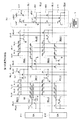
本実施の形態は強誘電体メモリとしての半導体記憶装置である。図1に構成例を示す。
図1に示すように、メモリユニットMUが、ビット線BL方向及びワード線WL方向に複数反復配置されてメモリアレイを構成する。
各メモリユニットMU11,MU12・・・は、それぞれ、一例として4つの強誘電体キャパシタCを有するものとしている。例えばメモリユニットMU11は、キャパシタC11〜C14を有する。もちろん、1つのメモリユニットMUにおけるキャパシタ数は4つに限られない。特に高集積化を目的とする場合は、より多数のキャパシタが設けられる。
【0030】
各メモリユニットMU内の構成は同様であるため、メモリユニットMU11によりその構成を説明する。
メモリユニットMU11では、複数の強誘電体キャパシタC11〜C14は、それぞれ異なるデータを記憶するメモリセルとなる。そしてこれらのキャパシタC11〜C14の各一端は共通ノード電極NEに接続される。
またそれぞれFETによりゲイン用トランジスタT11、読出スイッチT12,書込スイッチT13が設けられる。
ゲイン用トランジスタT11はディプレッション状態のNチャンネルMOS−FETであり、そのゲートは共通ノード電極NEに接続されている。さらにそのソース/ドレインは、一方がグランド(又はVcc等の電源線)に接続され、他方がFETによる読出スイッチT12を介してビット線BL1に接続されている。
読出スイッチT12のゲートは読出ワード線WLr1に接続されている。
また、FETによる書込スイッチT13のゲートは書込ワード線WLw1に接続され、ソース/ドレインは、一方が共通ノード電極NEに、他方がビット線BL1に接続されている。
各キャパシタC11〜C14は、それぞれの各他端は、それぞれプレート線PL1,PL2,PL3,PL4に接続されている。
【0031】
他のメモリユニットMUも、内部構成は同様であるが、接続されるワード線WL、ビット線BL、プレート線PLが、その配置位置に応じたものとなる。
【0032】
ワード線WL方向に並ぶ各メモリユニットにおいては、交互に、読出ワード線WLr、書込ワード線WLwが共有される。
例えばメモリユニットMU11、MU13では、読出ワード線WLr1が、これら各メモリユニットMU11、MU13の読出スイッチ(T12等)のゲートに接続され、また書込ワード線WLw1が各メモリユニットMU11、MU13の書込スイッチ(T13等)のゲートに接続される。
また例えばメモリユニットMU12、MU14では、読出ワード線WLr2が、各メモリユニットMU12、MU14の読出スイッチ(T22等)のゲートに接続され、また書込ワード線WLw2が各メモリユニットMU12、MU14の書込スイッチ(T23等)のゲートに接続される。
【0033】
ビット線BL方向に並ぶ各メモリユニットでは、ビット線BLが共有される。
例えばメモリユニットMU11、MU21には、ビット線BL1が、読出スイッチT2、書込スイッチT3を介して接続される。
各ビット線BL(BL1,BL2・・・)は、それぞれセンスアンプ2(2−1、2−2・・・)によって書込時に電圧印加され、また読出時に電位検出される。
センスアンプ2は、読出を行うビット線BLの電位と参照信号を比較して、読み出された値を判定する回路である。
【0034】
このようにメモリユニットMUを複数配置したメモリアレイ内には、ワード線方向にダミーユニット行10が設けられる。
このダミーユニット行10には、各ビット線BL1,BL2・・・に対応してダミーユニットdU(dU1,dU2・・・)が形成される。
各ダミーユニットdU内は、上記メモリユニットMU内のゲイン用トランジスタ(T11、T21・・・)と同一の構造とサイズを持つFETによるダミートランジスタdT11、dT21・・・が設けられ、またダミー読出スイッチdT12、dT22・・・が設けられる。
【0035】
ダミートランジスタdT11、dT21・・・の各ゲートは、参照電位線Lrefに接続されている。さらにそのソース/ドレインは、一方がグランド(又はVcc等の電源線)に接続され、他方がFETによるダミー読出スイッチdT12、dT22・・・を介してそれぞれ対応するビット線BL1、BL2・・・に接続されている。
ダミーユニット行10に対しては、一対のダミーワード線dWL1,dWL2が配され、各ダミーユニットが交互に接続される。
例えばダミーユニットdU1,dU3では、ダミー読出スイッチ(dT12等)のゲートはダミーワード線dWL1に接続され、ダミーユニットdU2,dU4では、ダミー読出スイッチ(dT22等)のゲートはダミーワード線dWL2に接続される。
【0036】
また参照電位Vrefを発生する参照電位発生回路1が設けられる。発生される参照電位Vrefは、参照電位線Lrefを介して各ダミーユニットdUのダミートランジスタdT11,dT21・・・のゲートに印加される。
発生される参照電位Vrefは、データ“1”、データ“0”それぞれが保持されたメモリセル(キャパシタC)からノードNEに発生する信号の中間レベルに設定された電位とされる。
【0037】
本例ではこのように、メモリユニットMUが複数配置されたメモリアレイ内に、ダミートランジスタdT11,dT21・・・を有するダミーユニットdUが配されるものとなる。
この場合のデータ読出は次のように行われる。
なお、この例ではメモリアレイ内に複数のセンスアンプ2−1,2−2・・・が並んでいるが、各センスアップ2に対して、一対のメモリユニットMUとダミーユニットdUが選択され、アクセスされる形になる。
【0038】
例えばメモリユニットMU11のキャパシタC11と、メモリユニットMU12のキャパシタC21からデータ読出を行う場合を例に挙げる。
この場合、プレート線PL11が選択されて高レベルに駆動される。すると、キャパシタC11,C21の記憶状態に応じて異なる信号が、各ゲイン用トランジスタT11、T21のゲートにそれぞれ印加される。
【0039】
ここで読出ワード線WLr1とダミーワード線dWL2を同時にオンとすることで、読出スイッチT12及びダミー読出スイッチdT22がオンとなるため、ゲイン用トランジスタT11がビット線BL1を駆動し、またダミートランジスタdT21がビット線BL2を駆動する。従ってビット線BL1には、キャパシタC11のデータに応じた読出電流が流れ、ビット線BL2には参照電位Vrefに基づく参照電流が流れて両者の電位が変動する。
これをセンスアンプ2−1で比較感知することで、メモリセル(キャパシタC11)の記憶値が判定される。
【0040】
続いて両ビット線BL1,BL2をイコライズし、今度は読出ワード線WLr2とダミーワード線dWL1を同時にオンとする。すると読出スイッチT22及びダミー読出スイッチdT12がオンとなるため、ゲイン用トランジスタT21がビット線BL2を駆動し、またダミートランジスタdT11がビット線BL1を駆動する。従ってビット線BL2には、キャパシタC21のデータに応じた読出電流が流れ、ビット線BL1には参照電位Vrefに基づく参照電流が流れて両者の電位が変動する。
これをセンスアンプ2−1で比較感知することで、メモリセル(キャパシタC21)の記憶値が判定される。
【0041】
このように本例の場合、或るビット線BL上のメモリユニットからのデータ読出の場合には、同一のセンスアンプ2に対応する他方のビット線BL上のダミーユニットdUによって参照信号が得られるものである。
ここでゲイン用トランジスタT11、T21・・・と、ダミートランジスタdT11,dT21・・・とは、同一セルアレイ内に存在し、互いに近接した場所にある。このため、それらの閾値の差はチップ間、ウェファー間、ロット間ばらつきの影響を受けず、チップ内ばらつきの影響も極めて小さい。従ってそれらのばらつきがセンスアンプ2による読出値の判定に影響を与えることはほとんどない。つまり、読み出しマージンを劣化させることは殆ど無い。
【0042】
なお、アクセスするメモリユニットMUとダミーユニットdUをできるだけ近接させるべく、同一のセルアレイ内に複数のダミーユニット行10を設け、アクセスユニットに近いダミーユニット行が参照ビット線を駆動するようにしてもよい。
【0043】
<第2の実施の形態>
図2に第2の実施の形態の構成例を示す。
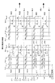
上記第1の実施の形態は、いわゆる折り返しビット線構成をとっているが、この図2の第2の実施の形態は、開放ビット線構成の例とするものである。
【0044】
センスアンプ2−1に対するビット線として、ビット線BL1−1、BL1−2が設けられ、またセンスアンプ2−2に対するビット線として、ビット線BL2−1、BL2−2が設けられる、といったように、一対のビット線BLがセンスアンプ2をはさんで隣接するセルアレイ内に形成される構造である。
【0045】
図示する各メモリユニットMU11、MU12、MU21、MU22は、それぞれビット線BL1−1、BL1−2、BL2−1、BL2−2上に配置されるメモリユニットとしている。
また、各ビット線BL1−1、BL1−2、BL2−1、BL2−2上には、それぞれダミーユニットdU11,dU12,dU21,dU22が設けられる。
各メモリユニットMU内の構成、及びダミーユニットdU内の構成は図1と同様である。
参照電位線Lrefは、各セルアレイに対してそれぞれ参照電位線Lref1,Lref2として設けられ、参照電位発生回路1によって参照電位Vrefが印加される。
【0046】
この構成の場合、読出動作時に、アクセスするメモリユニットMUに対応して参照信号を得るためのダミーユニットdUは、センスアンプ2を挟んで隣接するセルアレイ内に配置されていることになる。
【0047】
例えばメモリユニットMU11のキャパシタC11からデータ読出を行う場合、プレート線PL11が選択されて高レベルに駆動されると、キャパシタC11の記憶状態に応じて異なる信号が、ゲイン用トランジスタT11のゲートに印加される。
ここで読出ワード線WLr1とダミーワード線dWL2を同時にオンとすることで、ゲイン用トランジスタT11がビット線BL1−1を駆動し、またダミートランジスタdT21がビット線BL1−2を駆動する。従ってビット線BL1−1には、キャパシタC11のデータに応じた読出電流が流れ、ビット線BL1−2には参照電位Vrefに基づく参照電流が流れるため、センスアンプ2−1で比較感知することで、キャパシタC11の記憶値が判定される。
【0048】
またメモリユニットMU12のキャパシタC21からデータ読出を行う場合は、
プレート線PL21が高レベルに駆動され、キャパシタC21の記憶状態に応じて異なる信号が、ゲイン用トランジスタT21のゲートに印加される。
ここで読出ワード線WLr2とダミーワード線dWL1を同時にオンとすることで、ゲイン用トランジスタT21がビット線BL1−2を駆動し、またダミートランジスタdT11がビット線BL1−1を駆動する。従ってビット線BL1−2には、キャパシタC21のデータに応じた読出電流が流れ、ビット線BL1−1には参照電位Vrefに基づく参照電流が流れるため、センスアンプ2−1で比較感知することで、キャパシタC21の記憶値が判定される。
この実施の形態によっても、第1の実施の形態と同様の効果を得ることができる。
【0049】
<第3の実施の形態>
第3の実施の形態の構成を図3に示す。これは、ダミーユニットdUがメモリユニットMU内に設けられた構成例である。
【0050】
上記図1と同様に、例えばセンスアンプ2−1に対応する一対のビット線BL1,BL2において、ビット線BL1上にはメモリユニットMU11、MU21・・・が配置され、ビット線BL2上にはメモリユニットMU12、MU22・・・が配置される。
そして各メモリユニットMU内には、それぞれダミートランジスタ(dT11,dT21等)、及びダミー読出スイッチ(dT12,dT22等)を有して成るダミーユニットdU(dU11,dU12,dU21,dU22)が設けられている。
つまり、メモリユニットMUとダミーユニットdUが1:1で設けられているものである。
各ダミーユニットdUのダミートランジスタ(dT11,dT21等)のゲートには、上述した各実施の形態と同様に、参照電位発生回路1によって参照電位Vrefが供給される。
【0051】
書込ワード線WLw、読出ワード線WLrが、ワード線方向に並んだメモリユニットMUで交互に共用される(ワード線方向に隣接するメモリユニットMU同士は別のワード線WLに接続される)ことは図1と同様であるが、各メモリユニットMU内のダミーユニットdUに対してダミーワード線dWLは設けられず、読出ワード線WLrがダミーワード線として共用される。
例えばメモリユニットMU11のダミー読出スイッチdT12のゲートは、隣接するメモリユニット(例えばMU12)に対応する読出ワード線WLr2が接続され、また、メモリユニットMU12のダミー読出スイッチdT22のゲートは、隣接するメモリユニット(例えばMU11)に対応する読出ワード線WLr1が接続される。
【0052】
このような構成において、例えば一対のビット線上に配された一対のメモリユニット、例えばメモリユニットMU11とMU12は、互いに隣接しているか、または極めて近接した場所に配置されるものとなる。
そしてメモリセルへの読出アクセス時には互いのダミーユニットdUが相互に対応して動作することになる。
【0053】
例えばメモリユニットMU11のキャパシタC11と、メモリユニットMU12のキャパシタC21からデータ読出を行う場合を例に挙げる。
この場合、プレート線PL11が選択されて高レベルに駆動される。すると、キャパシタC11,C21の記憶状態に応じて異なる信号が、各ゲイン用トランジスタT11、T21のゲートにそれぞれ印加される。
【0054】
ここで読出ワード線WLr1をオンとすることで、ゲイン用トランジスタT11がビット線BL1を駆動し、またダミートランジスタdT21がビット線BL2を駆動する。従ってビット線BL1には、キャパシタC11のデータに応じた読出電流が流れ、ビット線BL2には参照電位Vrefに基づく参照電流が流れて両者の電位が変動する。これをセンスアンプ2−1で比較感知することで、メモリセル(キャパシタC11)の記憶値が判定される。
【0055】
続いて両ビット線BL1,BL2をイコライズし、今度は読出ワード線WLr2をオンとする。するとゲイン用トランジスタT21がビット線BL2を駆動し、またダミートランジスタdT11がビット線BL1を駆動する。従ってビット線BL2には、キャパシタC21のデータに応じた読出電流が流れ、ビット線BL1には参照電位Vrefに基づく参照電流が流れて両者の電位が変動する。これをセンスアンプ2−1で比較感知することで、メモリセル(キャパシタC21)の記憶値が判定される。
【0056】
本例では、このように対となったメモリユニットMUが互いに参照電位を提供しあう。そして同時に動作するゲイン用トランジスタとダミートランジスタ(例えばT11とdT21、或いはT21とdT11など)は極めて近接した場所に位置することになり、チップ内ばらつきについてもその影響はほぼ消滅し、その閾値差は10mV以下となる。従ってゲイン用トランジスタ(T11等)の閾値ばらつきが読み出しマージンを劣化させることは無い。
【0057】
<第4の実施の形態>
ところで十分な読出マージンを確保するには、ダミートランジスタdT11,dT21・・・のゲートに印加される参照電圧Vrefの調整も重要である。
強誘電体キャパシタをはじめ、多くのメモリ素子はその読出信号レベルに温度依存性をもつ。またメモリ素子自体の特性がチップ内、チップ間、ウェファー間、ロット間でばらつくので、参照電位発生回路1によって固定電位として参照電位Vrefを供給した場合、上記バラツキが全てマージン劣化につながる。
【0058】
これを考えると、ダミートランジスタdT11,dT21・・・のゲートに印加する参照電圧Vrefも、上記のようなメモリ素子のばらつきを相殺する機能を有することが望ましい。
この対策としては、通常の、ゲイン型メモリではないDRAMやFeRAMに見られるごとく、参照電位Vrefの発生手段として、メモリセルと同構造のダミーセルを使用することが有効である。
即ちダミーセルを使用して参照電位Vrefを発生させれば、参照電位もメモリセルからの読出信号と同様にメモリ素子のチップ間、ウェファー間、ロット間の特性ばらつきや温度依存性を有することになるため、これらが相殺されるためである。
【0059】
しかし検討の結果、ゲイン型メモリとダミーセルを組み合わせる場合、以下の2点に注意する必要があることが明らかとなった。
まずゲイン型メモリでは非常に小さなメモリ素子からの微小信号をゲインFETで増幅する形となるので、ダミーセル自体のチップ内特性ばらつきが重要なマージン劣化要因となる。
【0060】
次に、一般にゲイン型メモリにおいては、メモリセルが駆動する負荷容量は非常に小さいため、メモリセル自体がもつ寄生容量が全体の負荷容量に大きく寄与することになる。従って通常のメモリのように、メモリセルからの信号はメモリセルのサイズにリニアに依存しない。
例えば強誘電体メモリにおいて面積をA、単位面積あたりの分極量をP、単位面積あたりの常誘電成分(セルの寄生容量)をCs、駆動すべき負荷容量をCbとすると、メモリセルから読み出される信号Sは、
S=A・P/(A・Cs+Cb)
である。
【0061】
通常の強誘電体メモリであれば、駆動すべき負荷容量Cbは「A・Cs」に対して十分大きいため、
S=A・P/Cb
と考えることができ、つまり信号Sは面積Aにほぼ比例する。従ってダミーセルの面積を調整することで容易に“1”と“0”の中間信号を生成でき、実製品では殆どその手法が採用されている。しかしゲイン型メモリでは逆にCbが非常に小さいため、
S=A・P/(A・Cs)
となってしまい、つまり信号Sの面積依存性が殆ど無くなってしまう。ここでは簡単な1キャパシタ接続型を例にしたが、上記した実施の形態のように複数キャパシタでメモリユニットを構成しても同様である。即ちゲイン型メモリでは、セル面積を変えて信号レベルを調整するのは非常に困難である。このため、通常のメモリと同様の手法で、メモリセルを利用した参照電位発生を行うことは適切でない。
【0062】
そこで、このような点も考慮した上で、ダミーセルを使用して参照電位Vrefを発生させるようにした第4の実施の形態を図4で説明する。
この図4では、メモリユニットMUとしてはMU11〜MU14のみを示しているが、これらのメモリユニットMU及び図示を省略したメモリユニットMU(例えば図1のメモリユニットMU21〜MU24等)の構成や、各メモリユニットMUとワード線WL、ビット線BL、プレート線PLの接続状態は上述した図1と同様である。
図1の例では、ダミーユニット行10を示したが、このダミーユニット行10に相当する部分として、図4の場合、各ビット線BL1,BL2・・・に対応して図示する構成のダミーユニットdU1,dU2,dU3,dU4・・・が設けられる。
即ち各ダミーユニットdUは、メモリユニットMUのキャパシタCと同サイズのダミーキャパシタdCを有する構成とされる。
【0063】
例えばダミーユニットdU1について説明すると、このダミーユニットdU1には、4つのダミーキャパシタdC11〜dC14を有する。これらがメモリユニットMUのキャパシタCと同サイズのキャパシタとされる。
そしてこれらのダミーキャパシタdC11〜dC14の各一端は共通ノード電極dNEに接続される。
またダミープレート線dPL1〜dPL4が配され、ダミーキャパシタdC11〜dC14の各他端は、それぞれダミープレート線dPL1〜dPL4に接続される。
他のダミーユニットdU2,dU3・・・についても同様に、ダミーキャパシタdCが設けられる。そして各ダミーキャパシタdCは、それぞれ一端が、そのダミーユニットdU内の共通ノード電極dNEに接続され、他端がそれぞれダミープレート線dPL1〜dPL4に接続される。
【0064】
また、各ダミーユニットdU内には、上記メモリユニットMU内のゲイン用トランジスタ(T11、T21・・・)と同一の構造とサイズを持つFETによるダミートランジスタdT11、dT21・・・が設けられ、またダミー読出スイッチdT12、dT22・・・が設けられる。さらにダミー書込スイッチdT13、dT23・・・が設けられる。
【0065】
各ダミーユニットdU内において、各ダミートランジスタdT11、dT21・・・の各ゲートは、共通ノード電極dNEに接続されている。そしてそのソース/ドレインは、一方がグランド(又はVcc等の電源線)に接続され、他方がFETによるダミー読出スイッチdT12、dT22・・・を介してそれぞれ対応するビット線BL1、BL2・・・に接続されている。
【0066】
また、このようなダミーユニットdUが並んだダミーユニット行に対しては、一対のダミー読出ワード線dWLr1,dWLr2、及び一対のダミー書込ワード線dWLw1,dWLw2が配され、それぞれ、各ダミーユニットが交互に接続される。
例えばダミーユニットdU1,dU3では、ダミー読出スイッチ(dT12等)のゲートはダミー読出ワード線dWLr1に接続され、またダミー書込スイッチ(dT13等)のゲートはダミー書込ワード線dWLw1に接続される。
一方、ダミーユニットdU2,dU4では、ダミー読出スイッチ(dT22等)のゲートはダミー読出ワード線dWLr2に接続され、またダミー書込スイッチ(dT23等)のゲートはダミー書込ワード線dWLw2に接続される。
【0067】
また、同一のセンスアンプ2に対応する一対のビット線(例えばビット線BL1とBL2)に配されたダミーユニットdU同士で、各共通ノード電極dNEを短絡させるためのイコライズトランジスタTeqが設けられる。
例えばイコライズトランジスタTeq1は、ビット線BL1とBL2におけるダミーユニットdU1,dU2の各共通ノード電極dNEを短絡させるためのスイッチとなり、またイコライズトランジスタTeq2は、ビット線BL3とBL4におけるダミーユニットdU3,dU4の各共通ノード電極dNEを短絡させるためのスイッチとなる。
各イコライズトランジスタTeqのゲートにはイコライズ制御部11からイコライズ信号dEQが供給される。
【0068】
このように図4の構成では、ダミーユニットdUは、キャパシタサイズを含めてメモリユニットMUと同一の構成を有する。
そして、メモリユニットMUと同じビット線対(同一のセンスアンプ2に対応する一対のビット線)に、イコライズトランジスタTeqで短絡可能なダミーユニット対が接続されているものとなる。
ダミーユニット対、即ちイコライズトランジスタTeqにより接続される2つのダミーユニットでは、互いにダミープレート線dPLを共有するダミーキャパシタ対において、片側にはデータ“0”が、もう片側にはデータ“1”が記憶されている。
例えばダミーユニットdU1とdU2のダミーユニット対では、ダミーキャパシタdC11とdC21は、ダミープレート線dPL1を共有するが、このダミーキャパシタ対(dC11とdC21)の一方が“0”、他方が“1”とされる。
他のダミーキャパシタ対(dC12とdC22、dC13とdC23、dC14とdC24)も同様に、一方が“0”、他方が“1”とされる。
【0069】
このような構成において、例えばメモリユニットMU11のキャパシタC11,及びメモリユニットMU12のキャパシタC21からのデータ読出は次のように行われる。
まずプレート線PL11が選択されて高レベルになることで、キャパシタC11,C21の記憶状態に応じて異なる信号がゲイン用トランジスタT11、T21のゲートにそれぞれ印加される。
このとき同時にダミープレート線dPL1が選択され、ダミーキャパシタdC11,dC21から読み出された信号がダミートランジスタdT11,dT21のゲートにそれぞれ印加される。このとき、ダミートランジスタdT11,dT21の各ゲートに印加される信号の一方は“0”、他方は“1”に相当する信号となる。
【0070】
ここでイコライズ制御部11は、イコライズ制御信号dEQをイコライズトランジスタTeqのゲートに印加する。するとイコライズトランジスタTeq1がオンとされることで、ダミーユニットdU1の共通ノード電極dNEとダミーユニットdU2の共通ノード電極dNEがショートされる。つまりダミートランジスタdT11,dT21の各ゲートノードがショートされることになる。
これによって両ダミートランジスタdT11,dT21のゲートには“0”“1”のセル信号の中間値が印加される。
【0071】
ここで読出ワード線WLr1とダミー読出ワード線dWLr2を同時にオンとすることで、ゲイン用トランジスタT11がビット線BL1を駆動し、またダミートランジスタdT21がビット線BL2を駆動し、それぞれのビット線BL1,BL2に読出電流と参照電流が流れて両者の電位が変動する。これをセンスアンプ2−1で比較感知することで、メモリセル(キャパシタC11)の記憶値が判定される。
【0072】
さらに両ビット線BL1,BL2をイコライズした後、読出ワード線WLr2とダミー読出ワード線dWLr1を同時にオンとすることで、ゲイン用トランジスタT21がビット線BL2を駆動し、またダミートランジスタdT11がビット線BL1を駆動し、それぞれのビット線BL2,BL1に読出電流と参照電流が流れて両者の電位が変動する。これをセンスアンプ2−1で比較感知することで、メモリセル(キャパシタC21)の記憶値が判定される。
【0073】
他のキャパシタ対(キャパシタC12とキャパシタC22、キャパシタC13とキャパシタC23、キャパシタC14とキャパシタC24)においても、それぞれデータが相補的に記憶されたダミーキャパシタ対(ダミーキャパシタdC12とダミーキャパシタdC22、ダミーキャパシタdC13とダミーキャパシタdC23、ダミーキャパシタdC14とダミーキャパシタdC24)を用いて同様の読み出しを行う。
【0074】
このような第4の実施の形態では、ゲイン型メモリにおいて正確に“0”“1”の中間の参照電位を発生させることができる。そして第1〜第3の実施の形態と同様の効果に加え、さらにメモリセル自体の温度依存性や、その特性のチップ内、チップ間、ウェファー間、ロット間でばらつきに起因するマージン劣化も防止できるものとなる。
【0075】
なお、ここでの例では、一対のダミートランジスタ(例えばdT11とdT21)のゲートをショートさせたが、さらに複数対のダミートランジスタのゲートをまとめてショートさせるのが望ましい。即ち”0”が記憶されたダミーキャパシタからの信号を受けたダミートランジスタのゲートと、”1”が記憶されたダミーキャパシタからの信号と受けたダミートランジスタのゲートとを同数または略同数短絡させる。その場合、各ダミートランジスタのゲートに印加される電位の平準化が行われ、ダミーキャパシタdCの特性ばらつきに起因する参照電位自体のばらつきも大幅に低減できる。
【0076】
ところで、ゲイン型メモリではない通常のDRAMやFeRAMにおいては、参照電位Vrefの発生手段としてダミーセルを使用する例が提案されていることは先に述べた。それらでは、ダミーキャパシタの面積の調整により、参照電位Vrefを適値に定めるものである。ところが上述のように、本例のようなゲイン型メモリでは、ダミーキャパシタdCの面積の調整は、参照電位Vrefの発生に対して顕著な優位性がない。つまりゲイン型メモリにおいては、ダミーキャパシタ面積の調整でVrefを適値に定めるのは困難であり、通常のDRAMやFeRAMと同様の手法は適切ではない。
そこで図4の構成例のように、ゲイン型メモリにおいては、“0”“1”合成による参照電位発生方式を採用することが適切であり、これによってスケーリング性に優れるゲイン型メモリの特徴と適切な参照電位生成を両立させ、信頼性の高い超高集積メモリの実現に相乗的な効果をもたらすものである。
【0077】
また、この実施の形態では第1の実施の形態と同様、所謂折り返しビット線構成を例に参照電位の発生手法を述べているが、第2の実施の形態にあるような開放ビット線構成についても同様の手法が有効であることは言うまでもない。
【0078】
またゲイン型メモリにおいて、面積の依存性が微小であることを逆に利用して、ダミーキャパシタdCとしての強誘電体キャパシタ面積を通常のメモリセルとしてのキャパシタCより大きくしておけば、ダミーキャパシタdCのばらつきの影響をさらに低減することが出来る。
【0079】
<第5の実施の形態>
上記第4の実施の形態では、ダミートランジスタのゲートノードをショートさせることで“0”“1”合成を実現した。これはアクセスシーケンスの組み立てが容易な手法であるが、レイアウト的には細密なセルアレイ内にイコライズトランジスタTeqを埋め込む必要があり、その点では不利である。
一方“0”と“1”の参照電位、または参照電流を個別の参照ビット線に発生させ、両者を合成させて中間の参照電位を発生させても同様な効果が得られる。
さらにメモリセルとしてのキャパシタC(及びダミーキャパシタdC)からの読出信号のデータ保持時間や書き換え回数依存性を考慮した、本発明の第5の実施の形態を図5に示す。
【0080】
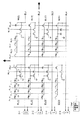
図5の例では、各メモリユニットMUは、図1や図4と同様にそれぞれワード線方向及びビット線方向に配置されている。
そしてこの例では、一対の参照ビット線dBL1,dBL2を配し、この参照ビット線dBL1,dBL2上に各ダミーユニットdUを配置する。
即ち参照ビット線dBL1上には、ダミーユニットdU11,dU21・・・が配置され、参照ビット線dBL2上には、ダミーユニットdU12,dU22・・・が配置される。
各ダミーユニットdUは、図4の場合と同様の構成となる。例えばダミーユニットdU11では、ダミーキャパシタdC11〜dC14、ダミートランジスタdT11、ダミー読出スイッチdT12、ダミー書込スイッチdT13を有する。
【0081】
各ダミーユニットdUでは、ワード線方向に並ぶメモリユニットMUとワード線WLを共有する。
例えばダミーユニットdU11,dU12では、各ダミー読出スイッチdT12,dT22のゲートには、メモリユニットMU11,MU12,MU13の各読出スイッチ(T12等)のゲートに接続された読出ワード線WLr1が接続される。
また例えばダミーユニットdU11,dU12では、各ダミー書込スイッチdT13,dT23のゲートには、メモリユニットMU11,MU12,MU13の各書込スイッチ(T13等)のゲートに接続された書込ワード線WLw1が接続される。
【0082】
また各ダミーユニットdUでは、ワード線方向に並ぶメモリユニットMUとプレート線PLを共有する。
例えばダミーユニットdU11,dU12では、各ダミーキャパシタdCには、メモリユニットMU11,MU12,MU13の各キャパシタCに対するプレート線PL11,PL12,PL13,PL14が接続される。
【0083】
この場合、ワード線方向に並ぶ2つのダミーユニットdUが、一組のダミーユニット対となる。
そして、ダミーユニット対となる2つのダミーユニットでは、互いにプレート線PLを共有するダミーキャパシタ対において、片側にはデータ“0”が、もう片側にはデータ“1”が記憶されている。
例えばダミーユニットdU11とdU12のダミーユニット対では、ダミーキャパシタdC11とdC21は、プレート線PL11を共有するが、このダミーキャパシタ対(dC11とdC21)の一方が“0”、他方が“1”とされる。
他のダミーキャパシタ対(dC12とdC22、dC13とdC23、dC14とdC24)も同様に、一方が“0”、他方が“1”とされる。
【0084】
また各ダミーキャパシタdCは、メモリユニットMUのキャパシタCとプレート線PLを共有していることから、各ROWアドレスごとにダミーキャパシタ対が設置されており、その片側に“0”、もう片側に“1”が記憶されている状態となっている。
【0085】
一対の参照ビット線dBL1,dBL2は、イコライズトランジスタTeq2によって短絡可能とされる。またイコライズトランジスタTeq1がオンとされることで、参照ビット線dBL1,dBL2の合成信号がセンスアンプ2−1、2−2・・・に供給されるものとなる。
【0086】
このような構成における読出動作を、メモリユニットMU11のキャパシタC11等、プレート線PL11に接続されたキャパシタCからのデータ読出を例に挙げて説明する。
プレート線PL11が選択されて高レベルとされると、そこに接続された各セルキャパシタの記憶状態に応じて異なる信号が対応する各メモリユニットMUのゲイン用トランジスタのゲートにそれぞれ印加される。例えばキャパシタC11からの信号がゲイン用トランジスタT11のゲートに印加される。
このとき同時にダミーキャパシタdC11,dC21から読み出された信号がダミートランジスタdT11,dT21のゲートに印加される。この場合、ダミートランジスタdT11,dT21の各ゲートに印加される信号の一方は“0”に相当する信号で、他方は“1”に相当する信号である。
【0087】
次に読出ワード線WLr1をオンとすることで、各メモリユニットMU11,MU12,MU13の各ゲイン用トランジスタ(T11等)が、それぞれビット線BL1,BL2,BL3を駆動する。さらにダミーユニットdU11,dU12の各ダミートランジスタdT11,dT21が、それぞれ参照ビット線dBL1,dBL2を駆動する。
ここでイコライズ制御部11がイコライズ制御信号dEQによりイコライズトランジスタTeq1,Teq2をオンとして参照ビット線dBL1,dBL2をショートさせれば、両者の電位が合成され、短絡された参照ビット線dBL1,dBL2上に“1”と“0”の中間の参照電位が発生する。また、両者を流れる電流は“1”と“0”の読み出し電流の総和である。
この電位を隣接するセンスアンプ群2−1,2−2,2−3に参照電位として配分する。各センスアンプ2−1,2−2,2−3は各々に接続されたビット線BL1,BL2,BL3の読出電位と、参照ビット線対dBL1,dBL2から配分された参照電位を比較して、読み出し値の判定を行う。
このようにして、例えばキャパシタC11等のメモリセルのデータが、センスアンプ2によって判定される。
【0088】
このような実施の形態でも、第4の実施の形態と同様の効果が得られ、読出マージンを向上させることができる。
そしてさらに、本例によれば、ダミーセル(ダミーキャパシタdC)を各ロウアドレスごとに設置し、アクセスしたメモリセル(キャパシタC)のロウアドレスに対応したダミーセル(ダミーキャパシタdC)を同時にアクセスすることになる。つまり各ダミーキャパシタdCは必ず対応するROWアドレスのキャパシタC行と同時にアクセスされる。従ってデータ保持時間も対応する同一行(同一プレート線PL上)のキャパシタCと同等に設定でき、アクセス回数も同じになる。
さらにセンスアンプ2とゲイン用トランジスタ(T11等)の距離と、センスアンプ2とダミートランジスタ(dT11等)の距離も同じになる。
従って、データ保持依存性、アクセス回数依存性、ビット線の電圧降下が全て相殺され、読出マージンの向上効果は、より顕著なものとなる。
【0089】
尚、ここでは各センスアンプ2−1,2−2・・・に参照信号を電圧として配分したが、電流を1/2にミラーして、参照電流として配分し、各センスアンプ2では、各ビット線BLを流れる電流と参照電流を比較して読出判定を行う構成としても良い。
【0090】
またここでは一対の参照ビット線dBL1,dBL2をショートさせたが、さらに複数対の参照ビット線dBLを一定数のセンスアンプ2おきに等間隔に配置し、それらをまとめてショートさせても良い。即ち”0”データが読み出された参照ビット線の信号と、”1” データが読み出された参照ビット線の信号とを同数または略同数短絡させる。このようにすれば参照電位または電流の平準化が行われ、ダミーキャパシタの特性ばらつきに起因する参照電位または参照電流のばらつきを大幅に低減できる。
【0091】
尚、このようなダミーユニットの配置は、ゲイン型ではない通常の強誘電体メモリにおいては適切とはいえない。
このように参照ビット線dBLから複数のセンスアンプ2に参照電位や電流を配分する場合、配分先のアクセスビット線BLと配分元の参照ビット線dBLとでは配線パタンが大きく異なる。
従ってある程度の負荷容量のアンバランスは避けられない。たとえビット線BLにキャパシタ等を付加してアンバランスを調整したとしても、完全なバランス実現は困難な上、負荷容量の大きい側に値を揃える必要がある。それをメモリセルの微細な信号で直接駆動しようとすると、かえって逆に大きなマージン劣化を生じさせてしまうためである。この傾向は特にDRAMや強誘電体メモリのように、キャパシタからの一定の電荷量でビット線BLに信号を生じさせるケースで顕著である。
一方、本例のようにゲイン用トランジスタでビット線BLを駆動するゲイン型メモリの場合、その駆動能力はメモリセルからの直接駆動よりはるかに高いため、ビット線BLの容量は通常のメモリより大きく設定でき、ビット線容量のアンバランスの影響を相対的に軽減できる。
【0092】
この場合、メモリセルが直接駆動するゲイン用トランジスタ(T11等)のゲートノードの負荷容量よりビット線容量を大きく設定するのが望ましい。
また、容量アンバランスの調整のためビット線BLに適切なMOSキャパシタ等を接続させると、さらに安定した読み出しが可能になる。
【0093】
また、ゲイン用トランジスタのドレイン側を電源に、ソース側をビット線BLに接続すれば、ビット線BLの電位Vbはビット線容量に関らず、
Vb=Vg−Vth
に収束する。VgはゲインFETのゲートに印加される信号レベル、Vthはゲイン用トランジスタの閾値である。
従ってビット線容量のアンバランスの影響を受けにくい。
【0094】
このようにゲイン型メモリでは、ビット線パタンのアンバランスの影響を大幅に低減でき、上述のダミーユニット構成を有効に活用できる。
但しそれでも参照電圧や参照電流の配分をあまりに過剰な数のセンスアンプ2に行うと、配線長等のアンバランスが無視できなくなる。従ってその配分はダミーユニットによる面積的オーバーヘッドとビット線容量のアンバランスのトレードオフを考慮してなされるべきであり、具体的にはセンスアンプ4個〜64個程度おきにダミーユニット対の列、および参照ビット線dBLの対を設けるのが望ましい。
【0095】
また、さらに複数対の参照ビット線dBLの電位または電流を合成するのが望ましい。例えばセルアレイに1024個のセンスアンプ2が並んでいるとすれば、32個おきに参照ビット線対を配置する。そのとき32対の参照ビット線対が挿入されるが、それらを全てショートさせれば合計64本の参照ビット線の電位が合成される。このときダミーキャパシタdCの特性ばらつきに起因する参照電位の変動幅は、単一の参照ビット線を使用するケースに比較して、(1/64)の平方根である(1/8)にまで低減される。従って読出マージン向上に、より有利となる。
【0096】
<本発明を適用できる他のゲイン型メモリの例>
以上の各実施の形態では、メモリセルが強誘電体キャパシタで構成される場合を例にとった。このタイプのゲイン型メモリでは、選択されたセルキャパシタが駆動する負荷容量は自身および非選択強誘電体キャパシタの特性が支配するが、これらは幾分かの弱反転した強誘電成分を含み、その値も温度依存性をもつ。従って第4、第5の実施の形態のように、メモリユニットと同構造のダミーユニットを設け、参照信号発生をダミーキャパシタで行うとともに、その駆動負荷にもダミーキャパシタを用いれば、駆動負荷の温度依存性も相殺できる効果を併せて獲得できる。
【0097】
但し本発明の適用範囲はメモリセルが強誘電体キャパシタで構成されたメモリのみに限るものではなく、微小なメモリセルの発生信号をFET(ゲイン用トランジスタ)のゲートに与え、そのFETでビット線BLを駆動することでデータを読み出すあらゆるゲイン型メモリに適用し得る。
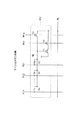
図6〜図8に本発明が適用可能な他のゲイン型メモリの例を示す。なお、各図においては、図9と同様の符号として、ゲイン用トランジスタをT1、読出スイッチをT2,書込スイッチをT3として示している。
【0098】
図6は常誘電体キャパシタC30がメモリセルとなっているDRAMである。キャパシタC30への蓄積電荷の有無で、ゲイン用トランジスタT1のゲートに接続されたノードNEへの入力信号が変化する。
この場合もメモリセル自身の寄生容量が負荷容量に大きな割合を占めるため、サイズの調整で適切な参照電位Vrefを発生させるのは困難である。さらにデータ保持時間により信号レベルが変化する問題も同様に存在する。従って上述した実施の形態と同手法の構成を採り、“1”と“0”を合成して中間の参照信号を得、またはROWアドレスごとにダミーセルを設けることは、非常に有効である。
【0099】
また、ゲイン型のメモリには上述のようにキャパシタによりゲイン用トランジスタのゲートを駆動するタイプの他に、記憶抵抗素子を用いてゲイン用トランジスタのゲートに信号電位を与えるタイプもある。その例を図7に示す。
抵抗素子R1はデータの記憶状態に応じて異なる抵抗値を示すメモリセルである。一方、抵抗素子R2は抵抗値を固定した参照用抵抗素子であり、リニア領域で動作させたMOSトランジスタや、拡散層やポリシリコン層等によって形成されている。
抵抗素子R1、R2の抵抗分割でゲイン用トランジスタT1のゲートに接続されたノードNEへの入力信号Vgが決まる。その値は両者の抵抗値をr1、r2とすると
Vg=Vcc・r1/(r1+r2)
である。
この例では記憶用抵抗素子R1がグランド側に、参照抵抗素子R2がVcc側に接続されているが、両者を入れ替えても良い。
【0100】
抵抗素子R1には例えば磁気ジャンクションを用いることが出来る。磁気ジャンクションはスピン方向を変えてデータを記憶する磁性膜と、スピン方向を固定した磁性膜とでトンネルバリアを挟んだ素子であり、記憶用磁性膜のスピン方向に応じて抵抗値が変化する。それを使用したメモリの例がISSCC(IEEE INTERNATIONAL SOLID−STATE CIRCUITS CONFERENCE)2000の論文番号7.2(R.Scheuerlein著, P.128)および7.3(M. Durlam著,P.130)に記述されている。
【0101】
また、抵抗素子R1には、例えばカルコゲナイド膜抵抗体を用いることもできる。カルコゲナイド膜は結晶状態が多結晶とアモルファス間を推移することでその抵抗率が変わるので、その膜を電極で挟んで抵抗素子とすれば良い。それを使用したメモリの例がISSCC2002の論文番号12.4(M. Gill著, P.202)に記載されている。
【0102】
また、抵抗素子R1には積層ゲートトランジスタや、チッ化膜ゲートトランジスタを用いることもできる。これらのトランジスタはEPROMとして使用されており、記憶状態に応じて閾値が変わることで、その抵抗値が変化する。さらにこれらを直列接続すれば、各々に独立したデータを記憶させることも出来る。
【0103】
このような抵抗型メモリの例においては、参照抵抗素子R2の温度特性とメモリセルである抵抗記憶素子R1の温度特性が異なる問題がある。従ってセルサイズの調整で抵抗値を調整する手法では、広い温度範囲で適切な参照電位Vrefを得るのは困難である。さらにデータ保持時間によりセルの抵抗値が変わり、信号レベルが変化する問題も存在する。従って“1”と“0”を合成して中間の参照信号を得、またはROWアドレスごとにダミーセルを設ける本発明の手法はセルにキャパシタを用いたケースと同様に有効である。
【0104】
また参照用抵抗素子の変わりに定電流源を用いても良い。その例を図8に示す。記憶抵抗素子R1に、定電流源として動作するNチャンネルMOS(T30)が接続されている。そのゲートには定電流源として飽和領域で動作するよう固定した電位が供給されている。このときゲイン用トランジスタT1のゲートに接続されたノードNEに印加される信号Vgは、R1の抵抗値をr1、T1を流れる電流をi1とすると、
Vg=Vcc−(r1・i1)
である。
このようなメモリの場合も、セルの抵抗値のバラツキ等に対応するため、“1”と“0”を合成して中間の参照信号を得、またはROWアドレスごとにダミーセルを設ける本発明の手法は有効である。
【0105】
以上、実施の形態、及び本発明が適用可能なゲイン型メモリの例を説明してきたが、本発明はさらなる応用が考えられる。
例えば、上記実施の形態では、各メモリセルが1ビット、即ち“0”“1”の2値を記憶するケースを想定してきた。しかし本発明は所謂多値を記憶する場合にも同様に適用できる。例えば各セルが2ビットを記憶する場合、ゲイン用トランジスタのゲートにはレベルの低い順に第1から第4の4レベルの信号が与えられることになり、その判定を行う必要が生じる。
この場合もダミーセルとダミートランジスタを使用し、例えば第2の信号と第3の信号の合成から第1の参照電位を発生させ、これを用いてまず読み出しセルが第1、第2の下位グループ、もしくは第3、第4の上位グループのいずれに属するかを判定する。
次に第1の信号と第2の信号の合成から第2の参照電位を、第3の信号と第4の信号の合成から第3の参照電位を発生させる。そして第2の参照電位を用いて下位グループ内でのレベル判別を、第3の参照電位を用いて上位グループ内でのレベル判別をそれぞれ行う。このようにして各セルの読み出し値を一意的に判定することができる。
【0106】
【発明の効果】
以上の説明からわかるように本発明によれば次のような効果が得られる。
一般にゲイン用トランジスタ(FET)の閾値にはロット間、ウェファー間の依存性があり、さらにはウェファー内でも強いチップ間依存性、さらにはチップ内の場所依存性がある。従って同一チップ内の互いに近傍に配置されたFET間では、その閾値差はほとんど生じることが無い。従って本発明のように、アクセスされるメモリセルに接続されたゲイン用トランジスタの近傍等に同サイズのダミートランジスタを配置し、それによって参照用とされる第2のビット線を駆動して、その第2のビット線の電位または電流を読み出し判定の参照信号として使用すれば、ゲイン用トランジスタの閾値ばらつきの影響を相殺することができ、結果として読み出しマージンを大幅に向上できるという効果がある。
【0107】
また、ダミートランジスタにはメモリユニットのメモリセルと同構造のダミーセルから信号を与えることで、メモリ素子のチップ間、ウェファー間、ロット間で生じる特性ばらつきを相殺することができる。さらにメモリセルからの読み出し信号と同様の温度依存性がダミートランジスタのゲート電位に生じることになる。従って温度依存性によるマージン劣化も防止できる。これによっても読み出しマージンを向上できる。
【0108】
また、さらに複数のダミートランジスタのゲートノードを一旦短絡させてから参照用とされるビット線を駆動することで、ダミーセルからの信号のチップ内ばらつきや、ダミートランジスタの残存ばらつき等により生じる参照電位または参照電流側のばらつきを統計的な平準化で低減できる。
同様の効果は複数の第2のビット線の電位または電流を合成して、それを参照信号として用いることでも達成できる。
特に、一対または複数対のダミートランジスタ、又は参照用の複数の第2のビット線を用い、第1の値(例えば「1」)を書き込んだダミーセルからの信号と、第2の値(例えば「0」)を書き込んだダミーセルからの信号を短絡してダミートランジスタのゲートに与えたり、或いは第1の値に応じたビット線電位または電流と、第2の値に応じたビット線電位または電流とを合成することで、正確に第1の値の読み出し時と第2の値の読み出し時の中間の参照信号レベルを発生することができ、上記平準化が適切に実現できる。これによって読み出しマージンを向上できる。
またこのことは、キャパシタサイズを調整して適切な中間信号を発生させるのが困難なゲイン型メモリでは特に有効となる。
またダミーセルの強誘電体キャパシタ面積を通常のメモリセルより大きくしておけば、ダミーキャパシタのばらつきの影響をさらに低減することができる。
【0109】
さらにゲイン用トランジスタのソース側にビット線を接続することで、最終的なビット線の電位は、ゲイン用トランジスタと閾値とそのゲートに加わるセルからの信号電位のみによって規定され、ビット線容量の影響を受けない。従って参照用とされた第2のビット線と読み出し用の第1のビット線とのパターン差によるビット線容量の差異の影響を低減できる。またはビット線容量自体を大きくする、つまりメモリセルが駆動するノードの容量よりビット線容量を大きくすることで、上記パターン差による影響を相対的に軽減することもできる。
【図面の簡単な説明】
【図1】本発明の第1の実施の形態の構成例の説明図である。
【図2】本発明の第2の実施の形態の構成例の説明図である。
【図3】本発明の第3の実施の形態の構成例の説明図である。
【図4】本発明の第4の実施の形態の構成例の説明図である。
【図5】本発明の第5の実施の形態の構成例の説明図である。
【図6】本発明を採用できるゲイン型メモリの例の説明図である。
【図7】本発明を採用できるゲイン型メモリの例の説明図である。
【図8】本発明を採用できるゲイン型メモリの例の説明図である。
【図9】ゲイン型メモリの構成の説明図である。
【図10】参照電位を用いて読出を行うゲイン型メモリの構成の説明図である。
【符号の説明】
1 参照電位発生回路、2,2−1,2−2・・・ センスアンプ、10 ダミーユニット行、11 イコライズ制御部、MU,MU11,MU12・・・ メモリユニット、WL ワード線、WLw1,WLw2・・・ 書込ワード線、WLr1,WLr2・・・ 読出ワード線、BL,BL1,BL2・・・ ビット線、PL,PL11,PL12・・・ プレート線、T11,T21 ゲイン用トランジスタ、T12,T22 読出スイッチ、T13,T23 書込スイッチ、dT11、dt12 ダミートランジスタ、dU,dU1,dU2 ダミーユニット[0001]
TECHNICAL FIELD OF THE INVENTION
The present invention relates to a semiconductor memory device, and more particularly to a reference potential generation technique for reading data.
[0002]
[Prior art]
With the miniaturization of semiconductor processing dimensions, instead of directly driving a bit line with a memory cell, a weak signal generated from a small memory cell is once received by the gate of an FET as a gain transistor, and the bit line is then applied to the bit line by the FET. Has attracted attention.
[0003]
Since such a gain-type memory is excellent in scalability, application to a DRAM or FeRAM is being studied. However, a similar method can be applied to other memories such as a flash memory and a magnetic memory (MRAM).
For example, in the following document, the present applicant has proposed a semiconductor memory device in which a plurality of ferroelectric capacitors are shared by one gain FET, and there is almost no area overhead due to installation of a gain circuit.
[Patent Document 1] JP-A-2002-197857
[0004]
FIG. 9 shows an example of a semiconductor memory device as this gain type memory.
The memory unit MU includes a plurality of ferroelectric capacitors C1, C2,... Cn connected to the common node electrode NE. Each of the capacitors C, C2,... Cn is a memory cell that stores different data.
The gain transistor T1 is an N-channel MOS-FET in a depletion state, and its gate is connected to the common node electrode NE. Further, one of the source / drain is connected to a power supply line such as Vcc or ground, and the other is connected to a bit line BL via a read switch T2 formed by an FET.
The gate of the read switch T2 is connected to the read word line WLr.
A write switch T3 of an FET is provided. The gate of the write switch T3 is connected to the write word line WLw. One of the source / drain is connected to the common node electrode NE, and the other is connected to the bit line BL. ing.
[0005]
One end of each of the capacitors C1, C2,... Cn is connected to the common node electrode NE. The other ends are connected to plate lines PL1, PL2,... PLn, respectively.
[0006]
When one bit is stored in one memory cell in such a gain-type memory, reading thereof requires some reference means for data determination.
An example of a conventional reference method will be described with reference to FIG.
[0007]
FIG. 10 shows a memory array in which the memory units MU as shown in FIG. 9 are repeatedly arranged in the bit line BL direction and the word line WL direction.
Each of the memory units MU11, MU12,... Has, for example, four ferroelectric capacitors C1 to C4.
[0008]
Each memory unit arranged in the word line WL direction shares a read word line WLr and a write word line WLw.
For example, in the memory units MU11, MU12, MU13, and MU14, the read word line WLr1 is connected to the gate of the read switch T2 of each of the memory units (MU11 to MU14), and the write word line WLw1 is connected to each of the memory units (MU11 to MU11). MU14) is connected to the gate of the write switch T3.
A voltage is applied to each word line WL by a word line drive circuit (not shown) according to an address to be accessed and write / read.
[0009]
Each memory unit arranged in the direction of the bit line BL shares the bit line BL.
For example, a bit line BL1 is connected to the memory units MU11 and MU21 via a read switch T2 and a write switch T3.
Each of the bit lines BL (BL1, BL2,...) Is applied with a voltage by the sense amplifier 2 (2-1, 2-2,...) At the time of writing, and a potential is detected at the time of reading.
[0010]
As shown in FIG. 9, each of the capacitors C1 to C4 in the memory unit MU is connected to the plate line PL.
For example, in the memory units MU11, MU12, MU13, and MU14, the capacitors C1 to C4 are connected to plate lines PL11 to PL14, respectively.
A predetermined voltage is applied to each plate line PL by a plate line driving circuit (not shown).
[0011]
Further, reference potential generating
The sense amplifier 2 (2-1, 2-2,...) Is a circuit that compares the potential of the bit line BL to be read with the reference potential Vref to determine a read value.
[0012]
In such a gain type memory, data reading is performed as follows.
For example, when reading data from the capacitor C1 of the memory unit MU11, the plate line PL11 is driven with the plate lines PL12 to PL14 fixed at 0V. Then, a signal corresponding to the polarization direction of the ferroelectric film forming the capacitor C1 is applied to the gate of the gain transistor T1.
Further, by selecting and turning on the read word line WLr1, the read switch T2 is turned on, and the gain transistor T1 is connected to the bit line BL1. As a result, the gain transistor T1 drives the bit line BL1, which has been equalized in advance to the Vcc potential, toward the ground. The driving capability depends on the gate potential, and varies depending on the storage state of the cell capacitor C1, that is, the polarization direction of the ferroelectric film. Therefore, the bit line potential changes depending on the storage state. The sense amplifier 2-1 compares the potential of the bit line BL1 with the reference potential Vref to determine the storage state of the cell capacitor C1, that is, whether the read value is "1" or "0". it can.
[0013]
In such a gain-type memory, the selected capacitor does not need to directly drive the bit line BL when reading data. Therefore, a large signal can be obtained even with a small capacitor, which is suitable for miniaturization.
[0014]
[Problems to be solved by the invention]
Usually, as shown in FIG. 10, a fixed potential generated by the reference
However, in that case, the following problem occurs.
[0015]
The threshold value of the gain transistor T1 has a distribution of a width of about several tens mV in the chip due to various factors in the manufacturing process.
Further, when the variation between the different chips in the wafer is included, the width is about 100 mV, and when the variation between the wafers and the lot is also included, the distribution width is 200 to 300 mV.
Accordingly, the driving capability of the bit line BL of the gain transistor T1 greatly varies, and even if the reference potential Vref is accurately generated, the read margin is significantly degraded.
[0016]
Further, the signal itself from the memory cell also varies among chips, between chips, between wafers, and between lots, and furthermore, the signal level also has a temperature dependency, so that each of them causes a deterioration of a read margin.
Further, when the memory unit MU to be accessed changes due to the difference in the ROW address of the memory cell to be accessed, and when the distance between the
In addition, depending on a storage element used for a memory cell, a signal may have access number dependence depending on fatigue. Further, the read signal level may change depending on the elapsed time from the writing, that is, the data holding time. All of these also directly lead to deterioration of the read margin.
[0017]
As described above, as long as the fixed potential or the fixed current is used as the reference potential Vref, it is inevitable that various variations in the potential or the current of the read bit line greatly deteriorate the read margin.
[0018]
[Means for Solving the Problems]
Therefore, the present invention proposes a method of generating a reference potential or a reference current that effectively cancels out each of the above-mentioned causes of variation.
[0019]
Therefore, the semiconductor memory device of the present invention drives one or a plurality of memory cells for generating a read potential according to a stored value at a predetermined node, and drives a first bit line based on the read potential generated at the node. A semiconductor memory device including a memory array in which a plurality of memory units each having a gain transistor are arranged. A second bit line; reference driving means for driving the second bit line by a dummy transistor having the same size as the gain transistor based on a reference potential; the first bit line and the second bit line; Read current determining means for determining the value of data read from the memory unit by comparing both currents flowing through the bit lines, or both potentials of the first bit line and the second bit line. Is provided.
[0020]
The second bit line is provided corresponding to one or a plurality of the memory units, and the reference driving means is provided corresponding to the second bit line. The read value determination means drives the first bit line corresponding to the memory unit to be read by the gain transistor, and drives the second bit line by the reference drive means. Then, the value of the data is determined by comparing the current flowing through both bit lines or the potential of both bit lines.
[0021]
The semiconductor device further includes a dummy cell having the same structure as the memory cell, wherein the reference potential is set to a potential of a signal read from the dummy cell and supplied to a gate of the dummy transistor.
A short circuit that includes a plurality of the second bit lines and a plurality of reference drive units for driving the corresponding second bit lines, and short-circuits the gates of the plurality of dummy transistors included in each of the reference drive units; Means.
The short-circuit means short-circuits the same number or substantially the same number of the gate to which the signal of the first value read from the dummy cell is supplied and the gate to which the signal of the second value read from the dummy cell is supplied. I do.
[0022]
In addition, a plurality of the second bit lines and a plurality of the reference drive units are provided, and a synthesizing unit for synthesizing signals respectively applied to the plurality of second bit lines is further provided. The value of the data is determined according to the signal generated by the combining means.
The synthesizing means is provided with a reference signal having a first value given to the second bit line by the reference driving means and given to the other second bit line by another reference driving means. The same number or approximately the same number of reference signals having the second value are combined.
[0023]
The predetermined node is connected to a gate of the gain transistor, and a load capacitance of the first bit line driven by the gain transistor and a load capacitance of the second bit line driven by the dummy transistor are: The load capacitance of the node driven by the gain transistor is larger than that of the node.
Further, the first bit line is connected to a source of the gain transistor, and the second bit line is connected to a source of the dummy transistor.
Further, the memory cell includes any of a ferroelectric capacitor, a paraelectric capacitor, a magnetoresistive element, a chalcogenide resistive element, a MONOS transistor, and a stacked gate transistor.
The memory cell includes a ferroelectric capacitor having one electrode connected to an independent control line and the other electrode connected to a common node electrode. The gain transistor has a gate connected to the common node electrode. Field effect transistor.
[0024]
A data read method according to the present invention comprises: a memory cell for generating a read signal corresponding to a stored value at a predetermined node; and a gain cell for driving a first bit line based on the read signal generated at the node. This is a data reading method in a semiconductor memory device including a memory array in which a plurality of memory units having transistors are arranged. Driving a second bit line different from the first bit line according to the supplied reference potential by using a dummy transistor having the same size as the gain transistor; Determining a value of data read from the memory unit by comparing currents flowing through the two bit lines or potentials of the first bit line and the second bit line, respectively.
The data reading method according to the present invention further comprises: one or more memory cells for generating a read signal corresponding to a storage value at a predetermined node; and a gain transistor for driving a bit line based on the read signal generated at the node. Is a data reading method in a semiconductor memory device provided with a plurality of memory units having a plurality of memory units, each bit line corresponding to one or a plurality of the memory units. Then, the first bit line corresponding to the memory unit to be read is driven by the gain transistor, and the second bit line different from the first bit line is supplied to the supplied reference potential. And reading the data from the memory unit to be read by comparing the currents flowing through the first and second bit lines or the potentials of the first and second bit lines. Determining the value of the data.
[0025]
That is, in the present invention as described above, first, in order to cancel the influence of the variation in the threshold value of the gain transistor, a dummy transistor having the same size as the gain transistor of the read cell is provided in the vicinity or the like, and the bit line (second Bit line). In this way, a reference signal as a reference potential or a reference current is generated in the second bit line, and the read value is determined by directly or indirectly comparing the state of the reference signal with the state of the read bit line (first bit line). It is.
Specifically, the dummy transistor is provided in the same or adjacent cell array as the gain transistor connected to the memory cell to be accessed. Alternatively, a gain transistor and a dummy transistor may be arranged in a pair in each memory unit, and the memory units arranged in pairs in the vicinity may provide a reference potential to each other.
In general, the threshold value of a transistor (FET) has lot-to-lot and wafer-to-wafer dependence, and furthermore, there is strong inter-chip dependence within a wafer, and further location dependence within a chip. Therefore, there is almost no threshold difference between FETs arranged close to each other in the same chip.
Therefore, a dummy transistor is arranged near a gain transistor connected to a memory cell to be accessed, thereby driving a reference bit line and using the potential or current of the bit line for reference in read determination. This makes it possible to cancel out the influence of the variation in the threshold value of the gain transistor.
[0026]
Further, in order to cancel the variation and the temperature dependency of the signal generated from the memory cell, it is preferable to apply a read signal from the dummy cell having the same structure as the memory cell to the gate of the dummy transistor.
Further, in order to level out variations in signals from the dummy cells, the gate nodes of the plurality of dummy transistors are once short-circuited, and then the reference bit line is driven. Alternatively, the potentials or currents of the plurality of second bit lines are combined to generate a read determination potential or current.
In particular, a signal from a dummy cell in which a first value (for example, "1") is written and a second value (for example, "0") are written using one or more pairs of dummy transistors or reference bit lines. The same number of signals from the dummy cells may be short-circuited and applied to the gate of the dummy transistor, or a second bit line potential or current corresponding to the first value and another second bit line potential corresponding to the second value Alternatively, the leveling can be appropriately performed by combining the same number of currents.
[0027]
Furthermore, in order to cancel the dependence of the sense potential of the sense amplifier (read value determination means) on the distance between the memory cell and the sense amplifier, the dependence on the data holding time of the signal generated from the memory, and the dependence on the number of accesses, A dummy cell may be arranged for each row address, a dummy cell corresponding to the row address of the accessed memory cell may be accessed, and its read signal may be supplied to the dummy transistor.
[0028]
BEST MODE FOR CARRYING OUT THE INVENTION
Hereinafter, first and second embodiments as a semiconductor memory device of the present invention will be described.
1 to 5 show the configuration of the first to fifth embodiments as a semiconductor memory device using a ferroelectric capacitor, and FIGS. 6 to 8 show the present invention. 5 shows another memory cell structure that can be employed.
In each figure, a word line is shown as a code including “WL” (for example, WLw1, WLr1, etc.), and a bit line is also shown as a code containing “BL”, and a plate line is also shown as a code containing “PL” Show.
For the word line WL and the plate line PL, a circuit section for driving those lines is not shown, but the word line WL is divided into an address which is accessed by a word line driving circuit (not shown) in a predetermined manner and a write / read operation. A corresponding voltage application is performed. A dummy word line (dWL) is also provided as a characteristic configuration of the embodiment, and the dummy word line dWL is also driven by a word line driving circuit.
The plate line PL (and the dummy plate line dPL) is applied with an address to be accessed in a predetermined manner by a plate line driving circuit (not shown) and a voltage application corresponding to writing / reading.
[0029]
<First embodiment>
This embodiment is a semiconductor memory device as a ferroelectric memory. FIG. 1 shows a configuration example.
As shown in FIG. 1, a plurality of memory units MU are repeatedly arranged in a bit line BL direction and a word line WL direction to form a memory array.
Each of the memory units MU11, MU12,... Has four ferroelectric capacitors C as an example. For example, the memory unit MU11 has capacitors C11 to C14. Of course, the number of capacitors in one memory unit MU is not limited to four. In particular, when the purpose is high integration, a larger number of capacitors are provided.
[0030]
Since the configuration inside each memory unit MU is the same, the configuration will be described using the memory unit MU11.
In the memory unit MU11, the plurality of ferroelectric capacitors C11 to C14 are memory cells each storing different data. One end of each of these capacitors C11 to C14 is connected to the common node electrode NE.
In addition, a gain transistor T11, a read switch T12, and a write switch T13 are provided by FETs.
The gain transistor T11 is an N-channel MOS-FET in a depletion state, and its gate is connected to the common node electrode NE. Further, one of the source / drain is connected to the ground (or a power supply line such as Vcc), and the other is connected to the bit line BL1 via a read switch T12 using an FET.
The gate of the read switch T12 is connected to the read word line WLr1.
The gate of the write switch T13 of the FET is connected to the write word line WLw1, and one of the source / drain is connected to the common node electrode NE and the other is connected to the bit line BL1.
The other ends of the capacitors C11 to C14 are connected to plate lines PL1, PL2, PL3, and PL4, respectively.
[0031]
The other memory units MU have the same internal configuration, but the connected word lines WL, bit lines BL, and plate lines PL are in accordance with the arrangement positions.
[0032]
In each memory unit arranged in the word line WL direction, the read word line WLr and the write word line WLw are alternately shared.
For example, in the memory units MU11 and MU13, the read word line WLr1 is connected to the gates of the read switches (T12 and the like) of these memory units MU11 and MU13, and the write word line WLw1 is connected to the write unit of each of the memory units MU11 and MU13. Connected to the gate of switch (T13 etc.).
Further, for example, in the memory units MU12 and MU14, the read word line WLr2 is connected to the gate of the read switch (T22 and the like) of each memory unit MU12 and MU14, and the write word line WLw2 is connected to the write of each memory unit MU12 and MU14. Connected to the gate of switch (T23 etc.).
[0033]
Each memory unit arranged in the direction of the bit line BL shares the bit line BL.
For example, a bit line BL1 is connected to the memory units MU11 and MU21 via a read switch T2 and a write switch T3.
Each of the bit lines BL (BL1, BL2,...) Is applied with a voltage by the sense amplifier 2 (2-1, 2-2,...) At the time of writing, and a potential is detected at the time of reading.
The
[0034]
A
In the
In each dummy unit dU, there are provided dummy transistors dT11, dT21... Formed by FETs having the same structure and size as the gain transistors (T11, T21...) In the memory unit MU. are provided.
[0035]
Each gate of the dummy transistors dT11, dT21,... Is connected to the reference potential line Lref. Further, one of the source / drain is connected to ground (or a power supply line such as Vcc), and the other is connected to corresponding bit lines BL1, BL2,... Via dummy read switches dT12, dT22. It is connected.
A pair of dummy word lines dWL1 and dWL2 are arranged for
For example, in the dummy units dU1 and dU3, the gate of the dummy read switch (dT12 and the like) is connected to the dummy word line dWL1, and in the dummy units dU2 and dU4, the gate of the dummy read switch (dT22 and the like) is connected to the dummy word line dWL2. You.
[0036]
Further, reference
The generated reference potential Vref is a potential set to an intermediate level of a signal generated at a node NE from a memory cell (capacitor C) holding data “1” and data “0”.
[0037]
In this example, as described above, a dummy unit dU having dummy transistors dT11, dT21,... Is arranged in a memory array in which a plurality of memory units MU are arranged.
Data reading in this case is performed as follows.
In this example, a plurality of sense amplifiers 2-1, 2-2,... Are arranged in the memory array. For each sense-
[0038]
For example, a case is described in which data is read from the capacitor C11 of the memory unit MU11 and the capacitor C21 of the memory unit MU12.
In this case, the plate line PL11 is selected and driven to a high level. Then, different signals depending on the storage states of the capacitors C11 and C21 are applied to the gates of the respective gain transistors T11 and T21.
[0039]
When the read word line WLr1 and the dummy word line dWL2 are simultaneously turned on, the read switch T12 and the dummy read switch dT22 are turned on. Therefore, the gain transistor T11 drives the bit line BL1, and the dummy transistor dT21 is turned on. Drive the bit line BL2. Therefore, a read current according to the data of the capacitor C11 flows through the bit line BL1, and a reference current based on the reference potential Vref flows through the bit line BL2, so that the potentials of the two change.
This is compared and sensed by the sense amplifier 2-1 to determine the stored value of the memory cell (capacitor C11).
[0040]
Subsequently, both bit lines BL1 and BL2 are equalized, and then the read word line WLr2 and the dummy word line dWL1 are simultaneously turned on. Then, the read switch T22 and the dummy read switch dT12 are turned on, so that the gain transistor T21 drives the bit line BL2, and the dummy transistor dT11 drives the bit line BL1. Therefore, a read current according to the data of the capacitor C21 flows through the bit line BL2, and a reference current based on the reference potential Vref flows through the bit line BL1, and both potentials change.
This is compared and sensed by the sense amplifier 2-1 to determine the stored value of the memory cell (capacitor C21).
[0041]
As described above, in the case of the present example, when data is read from a memory unit on a certain bit line BL, a reference signal is obtained by the dummy unit dU on the other bit line BL corresponding to the
Here, the gain transistors T11, T21,... And the dummy transistors dT11, dT21,... Exist in the same cell array and are located close to each other. Therefore, the difference between the threshold values is not affected by the variation between chips, between wafers, and between lots, and the effect of variation within a chip is extremely small. Therefore, these variations hardly affect the determination of the read value by the
[0042]
In order to make the memory unit MU to be accessed and the dummy unit dU as close as possible, a plurality of
[0043]
<Second embodiment>
FIG. 2 shows a configuration example of the second embodiment.
Although the first embodiment has a so-called folded bit line configuration, the second embodiment in FIG. 2 is an example of an open bit line configuration.
[0044]
Bit lines BL1-1 and BL1-2 are provided as bit lines for the sense amplifier 2-1 and bit lines BL2-1 and BL2-2 are provided as bit lines for the sense amplifier 2-2. , A pair of bit lines BL are formed in adjacent cell arrays with the
[0045]
The illustrated memory units MU11, MU12, MU21, MU22 are memory units arranged on bit lines BL1-1, BL1-2, BL2-1, BL2-2, respectively.
Dummy units dU11, dU12, dU21, and dU22 are provided on the bit lines BL1-1, BL1-2, BL2-1, and BL2-2, respectively.
The configuration in each memory unit MU and the configuration in the dummy unit dU are the same as those in FIG.
The reference potential line Lref is provided as reference potential lines Lref1 and Lref2 for each cell array, and the reference
[0046]
In the case of this configuration, the dummy unit dU for obtaining the reference signal corresponding to the memory unit MU to be accessed at the time of the read operation is arranged in the cell array adjacent to the
[0047]
For example, when data is read from the capacitor C11 of the memory unit MU11, when the plate line PL11 is selected and driven to a high level, a different signal depending on the storage state of the capacitor C11 is applied to the gate of the gain transistor T11. You.
Here, by turning on the read word line WLr1 and the dummy word line dWL2 simultaneously, the gain transistor T11 drives the bit line BL1-1, and the dummy transistor dT21 drives the bit line BL1-2. Therefore, a read current according to the data of the capacitor C11 flows through the bit line BL1-1, and a reference current based on the reference potential Vref flows through the bit line BL1-2. , The stored value of the capacitor C11 is determined.
[0048]
When data is read from the capacitor C21 of the memory unit MU12,
The plate line PL21 is driven to a high level, and a different signal is applied to the gate of the gain transistor T21 depending on the storage state of the capacitor C21.
Here, by turning on the read word line WLr2 and the dummy word line dWL1 simultaneously, the gain transistor T21 drives the bit line BL1-2, and the dummy transistor dT11 drives the bit line BL1-1. Therefore, a read current according to the data of the capacitor C21 flows through the bit line BL1-2, and a reference current based on the reference potential Vref flows through the bit line BL1-1. , The stored value of the capacitor C21 is determined.
According to this embodiment, the same effect as that of the first embodiment can be obtained.
[0049]
<Third embodiment>
FIG. 3 shows the configuration of the third embodiment. This is an example of a configuration in which the dummy unit dU is provided in the memory unit MU.
[0050]
As in the case of FIG. 1, for example, in a pair of bit lines BL1 and BL2 corresponding to the sense amplifier 2-1, memory units MU11, MU21... Are arranged on the bit line BL1, and a memory is arranged on the bit line BL2. The units MU12, MU22,... Are arranged.
In each memory unit MU, a dummy unit dU (dU11, dU12, dU21, dU22) including a dummy transistor (dT11, dT21, etc.) and a dummy read switch (dT12, dT22, etc.) is provided. I have.
That is, the memory unit MU and the dummy unit dU are provided at a ratio of 1: 1.
The reference potential Vref is supplied by the reference
[0051]
The write word line WLw and the read word line WLr are alternately shared by the memory units MU arranged in the word line direction (memory units MU adjacent in the word line direction are connected to another word line WL). Is the same as that of FIG. 1, but the dummy word line dWL is not provided for the dummy unit dU in each memory unit MU, and the read word line WLr is shared as the dummy word line.
For example, the gate of the dummy read switch dT12 of the memory unit MU11 is connected to the read word line WLr2 corresponding to the adjacent memory unit (for example, MU12), and the gate of the dummy read switch dT22 of the memory unit MU12 is connected to the adjacent memory unit. The read word line WLr1 corresponding to (for example, MU11) is connected.
[0052]
In such a configuration, for example, a pair of memory units arranged on a pair of bit lines, for example, the memory units MU11 and MU12 are arranged adjacent to each other or very close to each other.
Then, at the time of read access to the memory cell, the respective dummy units dU operate in correspondence with each other.
[0053]
For example, a case is described in which data is read from the capacitor C11 of the memory unit MU11 and the capacitor C21 of the memory unit MU12.
In this case, the plate line PL11 is selected and driven to a high level. Then, different signals depending on the storage states of the capacitors C11 and C21 are applied to the gates of the respective gain transistors T11 and T21.
[0054]
Here, by turning on the read word line WLr1, the gain transistor T11 drives the bit line BL1, and the dummy transistor dT21 drives the bit line BL2. Therefore, a read current according to the data of the capacitor C11 flows through the bit line BL1, and a reference current based on the reference potential Vref flows through the bit line BL2, so that the potentials of the two change. This is compared and sensed by the sense amplifier 2-1 to determine the stored value of the memory cell (capacitor C11).
[0055]
Subsequently, both bit lines BL1 and BL2 are equalized, and then the read word line WLr2 is turned on. Then, the gain transistor T21 drives the bit line BL2, and the dummy transistor dT11 drives the bit line BL1. Therefore, a read current according to the data of the capacitor C21 flows through the bit line BL2, and a reference current based on the reference potential Vref flows through the bit line BL1, and both potentials change. This is compared and sensed by the sense amplifier 2-1 to determine the stored value of the memory cell (capacitor C21).
[0056]
In this example, the memory units MU paired as described above provide a reference potential to each other. The gain transistor and the dummy transistor (for example, T11 and dT21, or T21 and dT11) which operate simultaneously are located very close to each other, and the influence of the in-chip variation almost disappears, and the threshold difference is reduced. It becomes 10 mV or less. Therefore, the threshold variation of the gain transistor (T11 or the like) does not degrade the read margin.
[0057]
<Fourth embodiment>
Incidentally, in order to secure a sufficient read margin, it is important to adjust the reference voltage Vref applied to the gates of the dummy transistors dT11, dT21,.
Many memory elements, such as ferroelectric capacitors, have temperature dependence on the read signal level. In addition, since the characteristics of the memory element itself vary among chips, between chips, between wafers, and between lots, when the reference
[0058]
Considering this, it is desirable that the reference voltage Vref applied to the gates of the dummy transistors dT11, dT21,... Also has a function of canceling the above-described variation in the memory elements.
As a countermeasure, it is effective to use a dummy cell having the same structure as the memory cell as a means for generating the reference potential Vref, as seen in a normal DRAM or FeRAM which is not a gain type memory.
That is, if the reference potential Vref is generated using the dummy cell, the reference potential also has the characteristic variation and the temperature dependency between chips, wafers, and lots of the memory element, similarly to the read signal from the memory cell. Therefore, these are offset.
[0059]
However, as a result of the study, it has been clarified that the following two points need to be paid attention when combining the gain type memory and the dummy cell.
First, in a gain-type memory, a small signal from a very small memory element is amplified by a gain FET, so that the in-chip characteristic variation of the dummy cell itself becomes an important margin deterioration factor.
[0060]
Next, in a gain-type memory, the load capacitance driven by a memory cell is generally very small, and the parasitic capacitance of the memory cell itself greatly contributes to the overall load capacitance. Therefore, unlike a normal memory, the signal from the memory cell does not depend linearly on the size of the memory cell.
For example, in a ferroelectric memory, if the area is A, the polarization amount per unit area is P, the paraelectric component per unit area (parasitic capacitance of the cell) is Cs, and the load capacitance to be driven is Cb, the data is read from the memory cell. The signal S is
S = A · P / (A · Cs + Cb)
It is.
[0061]
In the case of a normal ferroelectric memory, the load capacitance Cb to be driven is sufficiently larger than “A · Cs”.
S = AP / Cb
That is, the signal S is substantially proportional to the area A. Therefore, an intermediate signal of "1" and "0" can be easily generated by adjusting the area of the dummy cell, and this method is almost used in actual products. However, in the gain type memory, on the contrary, Cb is very small.
S = AP / (ACs)
That is, the area dependency of the signal S is almost eliminated. Here, a simple one-capacitor connection type is taken as an example, but the same applies to a case where a memory unit is composed of a plurality of capacitors as in the above embodiment. That is, it is very difficult to adjust the signal level by changing the cell area in the gain type memory. For this reason, it is not appropriate to generate a reference potential using a memory cell in the same manner as a normal memory.
[0062]
Therefore, a fourth embodiment in which the dummy cell is used to generate the reference potential Vref in consideration of such points will be described with reference to FIG.
In FIG. 4, only MU11 to MU14 are shown as the memory units MU. However, the configuration of these memory units MU and memory units MU (not shown) (for example, the memory units MU21 to MU24 in FIG. The connection states of the memory unit MU and the word lines WL, bit lines BL, and plate lines PL are the same as in FIG. 1 described above.
In the example of FIG. 1, the
That is, each dummy unit dU is configured to have a dummy capacitor dC having the same size as the capacitor C of the memory unit MU.
[0063]
For example, the dummy unit dU1 will be described. The dummy unit dU1 has four dummy capacitors dC11 to dC14. These are capacitors having the same size as the capacitor C of the memory unit MU.
One end of each of the dummy capacitors dC11 to dC14 is connected to the common node electrode dNE.
Dummy plate lines dPL1 to dPL4 are provided, and the other ends of dummy capacitors dC11 to dC14 are connected to dummy plate lines dPL1 to dPL4, respectively.
Similarly, dummy capacitors dC are provided for the other dummy units dU2, dU3,. One end of each dummy capacitor dC is connected to the common node electrode dNE in the dummy unit dU, and the other end is connected to each of the dummy plate lines dPL1 to dPL4.
[0064]
In each dummy unit dU, dummy transistors dT11, dT21... Formed by FETs having the same structure and size as the gain transistors (T11, T21...) In the memory unit MU are provided. Are provided. Dummy read switches dT12, dT22,. Further, dummy write switches dT13, dT23... Are provided.
[0065]
In each dummy unit dU, each gate of each dummy transistor dT11, dT21,... Is connected to a common node electrode dNE. One of the source / drain is connected to ground (or a power line such as Vcc), and the other is connected to corresponding bit lines BL1, BL2,... Via dummy read switches dT12, dT22. It is connected.
[0066]
A pair of dummy read word lines dWLr1 and dWLr2 and a pair of dummy write word lines dWLw1 and dWLw2 are arranged for a dummy unit row in which such dummy units dU are arranged. Connected alternately.
For example, in the dummy units dU1 and dU3, the gate of the dummy read switch (such as dT12) is connected to the dummy read word line dWLr1, and the gate of the dummy write switch (such as dT13) is connected to the dummy write word line dWLw1.
On the other hand, in the dummy units dU2 and dU4, the gate of the dummy read switch (dT22 and the like) is connected to the dummy read word line dWLr2, and the gate of the dummy write switch (dT23 and the like) is connected to the dummy write word line dWLw2. .
[0067]
An equalizing transistor Teq for short-circuiting each common node electrode dNE is provided between dummy units dU arranged on a pair of bit lines (for example, bit lines BL1 and BL2) corresponding to the
For example, the equalizing transistor Teq1 is a switch for short-circuiting the common node electrodes dNE of the dummy units dU1 and dU2 in the bit lines BL1 and BL2, and the equalizing transistor Teq2 is a switch for each of the dummy units dU3 and dU4 in the bit lines BL3 and BL4. This is a switch for short-circuiting the common node electrode dNE.
The equalizing signal dEQ is supplied from the equalizing
[0068]
As described above, in the configuration of FIG. 4, the dummy unit dU has the same configuration as the memory unit MU including the capacitor size.
Then, a dummy unit pair that can be short-circuited by the equalizing transistor Teq is connected to the same bit line pair as the memory unit MU (a pair of bit lines corresponding to the same sense amplifier 2).
In the dummy unit pair, that is, two dummy units connected by the equalizing transistor Teq, data “0” is stored on one side and data “1” is stored on the other side in the dummy capacitor pair sharing the dummy plate line dPL with each other. Have been.
For example, in the dummy unit pair of the dummy units dU1 and dU2, the dummy capacitors dC11 and dC21 share the dummy plate line dPL1, but one of the dummy capacitor pair (dC11 and dC21) is “0” and the other is “1”. Is done.
Similarly, one of the other dummy capacitor pairs (dC12 and dC22, dC13 and dC23, dC14 and dC24) is "0" and the other is "1".
[0069]
In such a configuration, for example, data reading from the capacitor C11 of the memory unit MU11 and the capacitor C21 of the memory unit MU12 is performed as follows.
First, when the plate line PL11 is selected and set to the high level, different signals are applied to the gates of the gain transistors T11 and T21 according to the storage states of the capacitors C11 and C21.
At this time, the dummy plate line dPL1 is selected at the same time, and signals read from the dummy capacitors dC11 and dC21 are applied to the gates of the dummy transistors dT11 and dT21, respectively. At this time, one of the signals applied to the gates of the dummy transistors dT11 and dT21 is a signal corresponding to "0" and the other is a signal corresponding to "1".
[0070]
Here, the equalizing
As a result, an intermediate value of the cell signals “0” and “1” is applied to the gates of the dummy transistors dT11 and dT21.
[0071]
Here, by turning on the read word line WLr1 and the dummy read word line dWLr2 at the same time, the gain transistor T11 drives the bit line BL1, and the dummy transistor dT21 drives the bit line BL2. The read current and the reference current flow through BL2, and the potentials of both of them fluctuate. This is compared and sensed by the sense amplifier 2-1 to determine the stored value of the memory cell (capacitor C11).
[0072]
Further, after equalizing both bit lines BL1 and BL2, the read word line WLr2 and the dummy read word line dWLr1 are simultaneously turned on, so that the gain transistor T21 drives the bit line BL2 and the dummy transistor dT11 drives the bit line BL1. , And a read current and a reference current flow through each of the bit lines BL2 and BL1, and the potentials of both of them fluctuate. This is compared and sensed by the sense amplifier 2-1 to determine the stored value of the memory cell (capacitor C21).
[0073]
In other capacitor pairs (capacitor C12 and capacitor C22, capacitor C13 and capacitor C23, and capacitor C14 and capacitor C24), dummy capacitor pairs (dummy capacitor dC12 and dummy capacitor dC22, dummy capacitor dC13) in which data are stored complementarily, respectively. And the dummy capacitor dC23, and the dummy capacitor dC14 and the dummy capacitor dC24).
[0074]
In such a fourth embodiment, an intermediate reference potential between “0” and “1” can be accurately generated in the gain memory. In addition to the same effects as those of the first to third embodiments, furthermore, the temperature dependency of the memory cell itself and the deterioration of the margin due to the variation in the characteristics among chips, chips, wafers, and lots are also prevented. You can do it.
[0075]
In this example, the gates of the pair of dummy transistors (for example, dT11 and dT21) are short-circuited. However, it is desirable that the gates of a plurality of pairs of dummy transistors be short-circuited. That is, the same number or substantially the same number of short-circuits are made between the gate of the dummy transistor that has received the signal from the dummy capacitor storing “0” and the gate of the dummy transistor that has received the signal from the dummy capacitor storing “1”. In this case, the potential applied to the gate of each dummy transistor is leveled, and the variation in the reference potential itself due to the variation in the characteristics of the dummy capacitor dC can be significantly reduced.
[0076]
By the way, as described above, in a normal DRAM or FeRAM which is not a gain type memory, an example using a dummy cell as a means for generating the reference potential Vref has been proposed. In these, the reference potential Vref is set to an appropriate value by adjusting the area of the dummy capacitor. However, as described above, in the gain-type memory according to the present example, the adjustment of the area of the dummy capacitor dC has no significant advantage over the generation of the reference potential Vref. That is, in the gain type memory, it is difficult to set Vref to an appropriate value by adjusting the area of the dummy capacitor, and a method similar to that of a normal DRAM or FeRAM is not appropriate.
Therefore, as in the configuration example of FIG. 4, in a gain type memory, it is appropriate to adopt a reference potential generation method based on “0” and “1” synthesis. And a synergistic effect for realizing a highly reliable ultra-highly integrated memory.
[0077]
Further, in this embodiment, as in the first embodiment, a method of generating a reference potential is described by taking a so-called folded bit line configuration as an example, but the open bit line configuration as in the second embodiment is described. Needless to say, a similar method is effective.
[0078]
Also, in the gain type memory, by utilizing the fact that the area dependency is minute, the area of the ferroelectric capacitor as the dummy capacitor dC is made larger than that of the capacitor C as the normal memory cell, and the dummy capacitor The effect of variation in dC can be further reduced.
[0079]
<Fifth embodiment>
In the fourth embodiment, “0” and “1” synthesis is realized by shorting the gate node of the dummy transistor. Although this is a method of easily assembling an access sequence, it is necessary to embed the equalizing transistor Teq in a fine cell array in terms of layout, which is disadvantageous in that point.
On the other hand, the same effect can be obtained by generating reference potentials or reference currents of “0” and “1” on individual reference bit lines and combining them to generate an intermediate reference potential.
FIG. 5 shows a fifth embodiment of the present invention in which the data retention time of the read signal from the capacitor C (and the dummy capacitor dC) as a memory cell and the dependence on the number of times of rewriting are taken into consideration.
[0080]
In the example of FIG. 5, the memory units MU are arranged in the word line direction and the bit line direction, respectively, as in FIGS.
In this example, a pair of reference bit lines dBL1 and dBL2 are arranged, and each dummy unit dU is arranged on the reference bit lines dBL1 and dBL2.
Are arranged on the reference bit line dBL1, and the dummy units dU12, dU22... Are arranged on the reference bit line dBL2.
Each dummy unit dU has the same configuration as in the case of FIG. For example, the dummy unit dU11 has dummy capacitors dC11 to dC14, a dummy transistor dT11, a dummy read switch dT12, and a dummy write switch dT13.
[0081]
Each dummy unit dU shares the word line WL with the memory units MU arranged in the word line direction.
For example, in the dummy units dU11 and dU12, the read word line WLr1 connected to the gate of each of the read switches (T12 and the like) of the memory units MU11, MU12 and MU13 is connected to the gate of each of the dummy read switches dT12 and dT22.
For example, in the dummy units dU11 and dU12, the gate of each of the dummy write switches dT13 and dT23 has the write word line WLw1 connected to the gate of each of the write switches (T13 and the like) of the memory units MU11, MU12 and MU13. Connected.
[0082]
Each dummy unit dU shares the plate line PL with the memory units MU arranged in the word line direction.
For example, in the dummy units dU11 and dU12, plate lines PL11, PL12, PL13 and PL14 for the respective capacitors C of the memory units MU11, MU12 and MU13 are connected to the respective dummy capacitors dC.
[0083]
In this case, two dummy units dU arranged in the word line direction form a pair of dummy units.
In the two dummy units forming the dummy unit pair, data “0” is stored on one side and data “1” is stored on the other side in the dummy capacitor pair sharing the plate line PL with each other.
For example, in the dummy unit pair of the dummy units dU11 and dU12, the dummy capacitors dC11 and dC21 share the plate line PL11. One of the dummy capacitor pair (dC11 and dC21) is "0" and the other is "1". You.
Similarly, one of the other dummy capacitor pairs (dC12 and dC22, dC13 and dC23, dC14 and dC24) is "0" and the other is "1".
[0084]
Further, since each dummy capacitor dC shares the plate line PL with the capacitor C of the memory unit MU, a dummy capacitor pair is provided for each ROW address, and “0” is set on one side and “D” is set on the other side. 1 "is stored.
[0085]
The pair of reference bit lines dBL1 and dBL2 can be short-circuited by the equalizing transistor Teq2. When the equalizing transistor Teq1 is turned on, a combined signal of the reference bit lines dBL1 and dBL2 is supplied to the sense amplifiers 2-1, 2-2,....
[0086]
A read operation in such a configuration will be described by taking data read from a capacitor C connected to the plate line PL11, such as the capacitor C11 of the memory unit MU11, as an example.
When the plate line PL11 is selected and set to a high level, a different signal is applied to the gate of the gain transistor of each memory unit MU corresponding to the storage state of each cell capacitor connected thereto. For example, a signal from the capacitor C11 is applied to the gate of the gain transistor T11.
At this time, signals read from the dummy capacitors dC11 and dC21 are simultaneously applied to the gates of the dummy transistors dT11 and dT21. In this case, one of the signals applied to the gates of the dummy transistors dT11 and dT21 is a signal corresponding to “0”, and the other is a signal corresponding to “1”.
[0087]
Next, when the read word line WLr1 is turned on, each gain transistor (T11 and the like) of each of the memory units MU11, MU12, and MU13 drives the bit lines BL1, BL2, and BL3, respectively. Further, the dummy transistors dT11 and dT21 of the dummy units dU11 and dU12 drive the reference bit lines dBL1 and dBL2, respectively.
Here, when the equalizing
This potential is distributed as a reference potential to the adjacent sense amplifier groups 2-1, 2-2, 2-3. Each of the sense amplifiers 2-1, 2-2, 2-3 compares the read potential of the bit line BL1, BL2, BL3 connected thereto with the reference potential distributed from the reference bit line pair dBL1, dBL2. The read value is determined.
In this way, the data of the memory cell such as the capacitor C11 is determined by the
[0088]
In such an embodiment, the same effect as in the fourth embodiment can be obtained, and the read margin can be improved.
Further, according to this example, a dummy cell (dummy capacitor dC) is provided for each row address, and a dummy cell (dummy capacitor dC) corresponding to the row address of the accessed memory cell (capacitor C) is simultaneously accessed. Become. That is, each dummy capacitor dC is always accessed at the same time as the capacitor C row of the corresponding ROW address. Accordingly, the data retention time can be set to be equal to that of the corresponding capacitor C on the same row (on the same plate line PL), and the number of accesses is the same.
Further, the distance between the
Therefore, the data retention dependency, the access count dependency, and the bit line voltage drop are all canceled out, and the effect of improving the read margin becomes more remarkable.
[0089]
Here, the reference signal is distributed as a voltage to each of the sense amplifiers 2-1, 2-2,..., But the current is mirrored to 1 / and distributed as a reference current. A configuration in which the read determination is performed by comparing the current flowing through the bit line BL with the reference current may be employed.
[0090]
Although a pair of reference bit lines dBL1 and dBL2 are short-circuited here, a plurality of pairs of reference bit lines dBL may be further arranged at regular intervals for a fixed number of
[0091]
Incidentally, such an arrangement of the dummy units is not appropriate for a normal non-gain type ferroelectric memory.
When the reference potential and the current are distributed from the reference bit line dBL to the plurality of
Therefore, some imbalance in load capacity cannot be avoided. Even if the imbalance is adjusted by adding a capacitor or the like to the bit line BL, it is difficult to achieve perfect balance, and it is necessary to adjust the value to the side with the larger load capacity. This is because, if it is attempted to drive it directly with the fine signal of the memory cell, on the contrary, a large margin deterioration is caused. This tendency is particularly remarkable in a case where a signal is generated on the bit line BL with a fixed amount of charge from a capacitor, such as a DRAM or a ferroelectric memory.
On the other hand, in the case of the gain type memory in which the bit line BL is driven by the gain transistor as in this example, the driving capability is much higher than the direct drive from the memory cell, so that the capacity of the bit line BL is larger than that of the normal memory. The influence of the imbalance of the bit line capacitance can be relatively reduced.
[0092]
In this case, it is desirable to set the bit line capacitance larger than the load capacitance of the gate node of the gain transistor (T11 or the like) directly driven by the memory cell.
Further, if an appropriate MOS capacitor or the like is connected to the bit line BL for adjusting the capacitance imbalance, more stable reading can be performed.
[0093]
Further, if the drain side of the gain transistor is connected to the power supply and the source side is connected to the bit line BL, the potential Vb of the bit line BL is independent of the bit line capacitance.
Vb = Vg-Vth
Converges to Vg is the signal level applied to the gate of the gain FET, and Vth is the threshold value of the gain transistor.
Therefore, it is hardly affected by the unbalance of the bit line capacitance.
[0094]
As described above, in the gain type memory, the influence of the imbalance of the bit line pattern can be significantly reduced, and the above-described dummy unit configuration can be effectively used.
However, if the distribution of the reference voltage and the reference current is performed to an excessively large number of
[0095]
It is desirable to further combine the potentials or currents of a plurality of pairs of reference bit lines dBL. For example, if 1024
[0096]
<Example of other gain type memory to which the present invention can be applied>
In each of the above embodiments, the case where the memory cell is formed of a ferroelectric capacitor is taken as an example. In this type of gain type memory, the load capacitance driven by the selected cell capacitor is governed by the characteristics of itself and the non-selected ferroelectric capacitor, which contain some weakly inverted ferroelectric components and The value also has temperature dependence. Therefore, as in the fourth and fifth embodiments, a dummy unit having the same structure as that of the memory unit is provided, the reference signal is generated by the dummy capacitor, and the dummy load is used as the driving load. Dependencies can also be offset.
[0097]
However, the application range of the present invention is not limited to a memory in which a memory cell is formed of a ferroelectric capacitor. A signal generated by a minute memory cell is given to the gate of a FET (gain transistor), and the FET is used to generate a bit line. The present invention can be applied to any gain type memory that reads data by driving the BL.
6 to 8 show examples of other gain memories to which the present invention can be applied. In each figure, the same reference numerals as those in FIG. 9 denote the gain transistor as T1, the read switch as T2, and the write switch as T3.
[0098]
FIG. 6 shows a DRAM in which the paraelectric capacitor C30 is a memory cell. The input signal to the node NE connected to the gate of the gain transistor T1 changes depending on the presence or absence of the charge stored in the capacitor C30.
Also in this case, since the parasitic capacitance of the memory cell itself accounts for a large proportion of the load capacitance, it is difficult to generate an appropriate reference potential Vref by adjusting the size. Further, there is a problem that the signal level changes depending on the data holding time. Therefore, it is very effective to adopt a configuration of the same method as in the above-described embodiment, obtain an intermediate reference signal by combining "1" and "0", or provide a dummy cell for each ROW address.
[0099]
In addition to the type in which the gate of the gain transistor is driven by the capacitor as described above, there is also a type in which a signal potential is applied to the gate of the gain transistor using a storage resistor element. An example is shown in FIG.
The resistance element R1 is a memory cell having a different resistance value according to the data storage state. On the other hand, the resistance element R2 is a reference resistance element having a fixed resistance value, and is formed of a MOS transistor operated in a linear region, a diffusion layer, a polysilicon layer, or the like.
The input signal Vg to the node NE connected to the gate of the gain transistor T1 is determined by the resistance division of the resistance elements R1 and R2. Assuming that their resistance values are r1 and r2,
Vg = Vcc · r1 / (r1 + r2)
It is.
In this example, the storage resistance element R1 is connected to the ground side and the reference resistance element R2 is connected to the Vcc side, but both may be interchanged.
[0100]
For example, a magnetic junction can be used for the resistance element R1. A magnetic junction is an element in which a tunnel barrier is sandwiched between a magnetic film that stores data by changing the spin direction and a magnetic film that fixes the spin direction. The resistance value changes according to the spin direction of the magnetic film for storage. Examples of a memory using the same are described in ISSCC (IEEE INTERNAL SOLID-STATE CIRCUITS CONFERENCE) 2000, article numbers 7.2 (R. Schuerlein, P. 128) and 7.3 (M. Durlam, P. 130). It has been described.
[0101]
Further, for example, a chalcogenide film resistor can be used for the resistance element R1. Since the resistivity of the chalcogenide film changes when the crystal state changes between polycrystalline and amorphous, the film may be sandwiched between electrodes to form a resistance element. An example of a memory using the same is described in ISSCC 2002, article number 12.4 (M. Gill, p. 202).
[0102]
In addition, a laminated gate transistor or a nitride film gate transistor can be used as the resistance element R1. These transistors are used as an EPROM, and the threshold value changes according to the storage state, so that the resistance value changes. If these are connected in series, independent data can be stored in each of them.
[0103]
In such an example of the resistance type memory, there is a problem that the temperature characteristic of the reference resistance element R2 is different from the temperature characteristic of the resistance storage element R1 as a memory cell. Therefore, it is difficult to obtain an appropriate reference potential Vref over a wide temperature range by the technique of adjusting the resistance value by adjusting the cell size. Further, there is a problem that the resistance value of the cell changes according to the data holding time, and the signal level changes. Therefore, the method of the present invention in which "1" and "0" are combined to obtain an intermediate reference signal, or a dummy cell is provided for each ROW address, is as effective as the case where a capacitor is used for a cell.
[0104]
Further, a constant current source may be used instead of the reference resistance element. An example is shown in FIG. An N-channel MOS (T30) operating as a constant current source is connected to the storage resistance element R1. The gate is supplied with a fixed potential as a constant current source so as to operate in a saturation region. At this time, the signal Vg applied to the node NE connected to the gate of the gain transistor T1 is as follows, assuming that the resistance value of R1 is r1 and the current flowing through T1 is i1.
Vg = Vcc− (r1 · i1)
It is.
Even in the case of such a memory, the method of the present invention in which "1" and "0" are combined to obtain an intermediate reference signal, or a dummy cell is provided for each ROW address, in order to cope with variations in the resistance value of the cell. Is valid.
[0105]
The embodiment and the example of the gain type memory to which the present invention can be applied have been described above, but the present invention can be further applied.
For example, in the above embodiment, a case has been assumed in which each memory cell stores one bit, that is, a binary value of “0” or “1”. However, the present invention can be similarly applied to a case where so-called multi-values are stored. For example, when each cell stores 2 bits, first to fourth four-level signals are given to the gate of the gain transistor in ascending order of level, and it is necessary to make a determination.
In this case as well, a dummy cell and a dummy transistor are used to generate a first reference potential from, for example, the synthesis of the second signal and the third signal, and the readout cell is used first to cause the read cell to operate in the first and second lower groups. Alternatively, it is determined which of the third and fourth upper groups belongs.
Next, a second reference potential is generated by combining the first signal and the second signal, and a third reference potential is generated by combining the third signal and the fourth signal. Then, level determination in the lower group is performed using the second reference potential, and level determination in the upper group is performed using the third reference potential. In this way, the read value of each cell can be uniquely determined.
[0106]
【The invention's effect】
As can be seen from the above description, according to the present invention, the following effects can be obtained.
In general, the threshold value of the gain transistor (FET) has lot-to-lot and wafer-to-wafer dependence, and also has a strong inter-chip dependence within the wafer and a location dependence within the chip. Therefore, there is almost no threshold difference between FETs arranged close to each other in the same chip. Therefore, as in the present invention, a dummy transistor of the same size is arranged near a gain transistor connected to a memory cell to be accessed, and the second bit line used as a reference is driven by the dummy transistor. If the potential or current of the second bit line is used as a reference signal for read determination, it is possible to cancel the influence of threshold variation of the gain transistor, and as a result, it is possible to greatly improve the read margin.
[0107]
Further, by supplying a signal from the dummy cell having the same structure as that of the memory cell of the memory unit to the dummy transistor, it is possible to cancel the characteristic variation occurring between chips, wafers, and lots of the memory element. Further, the same temperature dependence as the read signal from the memory cell occurs in the gate potential of the dummy transistor. Therefore, it is possible to prevent margin deterioration due to temperature dependency. This can also improve the read margin.
[0108]
Further, by short-circuiting the gate nodes of the plurality of dummy transistors once and then driving the bit line used as a reference, variations in the signal from the dummy cells within the chip, variations in the reference potential caused by variations in the remaining dummy transistors, etc. Variations on the reference current side can be reduced by statistical leveling.
A similar effect can also be achieved by combining the potentials or currents of a plurality of second bit lines and using them as a reference signal.
In particular, a signal from a dummy cell in which a first value (eg, “1”) is written using a pair or a plurality of pairs of dummy transistors or a plurality of second bit lines for reference, and a second value (eg, “ 0 ") is written to the gate of the dummy transistor by short-circuiting the signal from the dummy cell, or a bit line potential or current according to the first value and a bit line potential or current according to the second value. , The reference signal level intermediate between the reading of the first value and the reading of the second value can be accurately generated, and the leveling can be appropriately realized. Thereby, the read margin can be improved.
This is particularly effective in a gain-type memory in which it is difficult to generate an appropriate intermediate signal by adjusting the capacitor size.
If the area of the ferroelectric capacitor of the dummy cell is made larger than that of a normal memory cell, the influence of the variation of the dummy capacitor can be further reduced.
[0109]
Furthermore, by connecting the bit line to the source side of the gain transistor, the final bit line potential is determined only by the gain transistor, the threshold value, and the signal potential from the cell applied to its gate, and the influence of the bit line capacitance Not receive. Therefore, it is possible to reduce the influence of the difference in bit line capacitance due to the pattern difference between the second bit line used for reference and the first bit line for reading. Alternatively, by increasing the bit line capacitance itself, that is, by making the bit line capacitance larger than the capacitance of the node driven by the memory cell, the influence of the pattern difference can be relatively reduced.
[Brief description of the drawings]
FIG. 1 is an explanatory diagram of a configuration example according to a first embodiment of the present invention.
FIG. 2 is an explanatory diagram of a configuration example according to a second embodiment of the present invention.
FIG. 3 is an explanatory diagram of a configuration example according to a third embodiment of the present invention.
FIG. 4 is an explanatory diagram of a configuration example according to a fourth embodiment of the present invention.
FIG. 5 is an explanatory diagram of a configuration example according to a fifth embodiment of the present invention.
FIG. 6 is an explanatory diagram of an example of a gain type memory to which the present invention can be applied.
FIG. 7 is an explanatory diagram of an example of a gain type memory to which the present invention can be applied.
FIG. 8 is an explanatory diagram of an example of a gain type memory that can employ the present invention.
FIG. 9 is an explanatory diagram of a configuration of a gain type memory.
FIG. 10 is an explanatory diagram of a configuration of a gain memory that performs reading using a reference potential.
[Explanation of symbols]
1 Reference potential generation circuit, 2, 2-1, 2-2,... Sense amplifier, 10 dummy unit row, 11 Equalization control unit, MU, MU11, MU12,. .. Write word lines, WLr1, WLr2 ... Read word lines, BL, BL1, BL2 ... Bit lines, PL, PL11, PL12 ... Plate lines, T11, T21 Gain transistors, T12, T22 Read Switch, T13, T23 Write switch, dT11, dt12 Dummy transistor, dU, dU1, dU2 Dummy unit
Claims (13)
第2のビット線と、
参照電位に基づいて上記ゲイン用トランジスタと同サイズのダミートランジスタにより上記第2のビット線を駆動する参照用駆動手段と、
上記第1のビット線と上記第2のビット線をそれぞれ流れる両電流、又は上記第1のビット線と上記第2のビット線の両電位を比較することにより上記メモリユニットから読み出されたデータの値を判定する読出値判定手段と、
を備えたことを特徴とする半導体記憶装置。A memory unit having one or more memory cells for generating a read potential according to a stored value at a predetermined node and a gain transistor for driving a first bit line based on the read potential generated at the node, In a semiconductor memory device including a plurality of arranged memory arrays,
A second bit line;
Reference driving means for driving the second bit line by a dummy transistor having the same size as the gain transistor based on a reference potential;
Data read from the memory unit by comparing both currents flowing through the first bit line and the second bit line, respectively, or both potentials of the first bit line and the second bit line. Reading value determining means for determining the value of
A semiconductor memory device comprising:
上記参照用駆動手段は、上記第2のビット線に対応して設けられ、
上記読出値判定手段は、読み出し対象とされた上記メモリユニットに対応する上記第1のビット線を上記ゲイン用トランジスタにより駆動すると共に、上記第2のビット線を上記参照用駆動手段で駆動して、両ビット線に流れる電流又は両ビット線の電位を比較することにより上記データの値を判定することを特徴とする請求項1に記載の半導体記憶装置。The second bit line is provided corresponding to one or a plurality of the memory units,
The reference driving means is provided corresponding to the second bit line,
The read value determination means drives the first bit line corresponding to the memory unit to be read by the gain transistor, and drives the second bit line by the reference drive means. 2. The semiconductor memory device according to claim 1, wherein the value of the data is determined by comparing a current flowing through both bit lines or a potential of both bit lines.
上記参照電位は、該ダミーセルから読み出された信号の電位とされると共に、上記ダミートランジスタのゲートに供給されることを特徴とする請求項1に記載の半導体記憶装置。Further comprising a dummy cell having the same structure as the memory cell,
2. The semiconductor memory device according to claim 1, wherein the reference potential is a potential of a signal read from the dummy cell and is supplied to a gate of the dummy transistor.
該複数の第2のビット線にそれぞれ与えられた信号を合成する合成手段をさらに備え、
上記読出値判定手段は、上記合成手段により生成された信号に応じて上記データの値を判定することを特徴とする請求項1に記載の半導体記憶装置。A plurality of the second bit lines and the reference driving means are provided,
A synthesizing means for synthesizing signals respectively applied to the plurality of second bit lines;
2. The semiconductor memory device according to claim 1, wherein said read value determination means determines the value of said data in accordance with a signal generated by said synthesis means.
上記ゲイン用トランジスタにより駆動される上記第1のビット線および上記ダミートランジスタにより駆動される上記第2のビット線の負荷容量が、上記ゲイン用トランジスタにより駆動される上記ノードの負荷容量より大きいことを特徴とする請求項1に記載の半導体記憶装置。The predetermined node is connected to a gate of the gain transistor,
The load capacity of the first bit line driven by the gain transistor and the load capacity of the second bit line driven by the dummy transistor are larger than the load capacity of the node driven by the gain transistor. The semiconductor memory device according to claim 1, wherein:
上記第2のビット線は上記ダミートランジスタのソースに接続されていることを特徴とする請求項1に記載の半導体記憶装置。The first bit line is connected to a source of the gain transistor,
2. The semiconductor memory device according to claim 1, wherein said second bit line is connected to a source of said dummy transistor.
上記ゲイン用トランジスタは、ゲートが上記共通ノード電極に接続された電界効果トランジスタからなることを特徴とする請求項1に記載の半導体記憶装置。The memory cell includes a ferroelectric capacitor having one electrode connected to an independent control line and the other electrode connected to a common node electrode,
2. The semiconductor memory device according to claim 1, wherein said gain transistor comprises a field effect transistor having a gate connected to said common node electrode.
上記ゲイン用トランジスタと同サイズのダミートランジスタにより、供給される参照電位に応じて上記第1のビット線と異なる第2のビット線を駆動するステップと、
上記第1のビット線と上記第2のビット線をそれぞれ流れる電流、又は上記第1のビット線と上記第2のビット線の各電位を比較することにより上記メモリユニットから読み出されたデータの値を判定するステップとを有することを特徴とするデータ読み出し方法。A memory unit having one or more memory cells for generating a read signal corresponding to a stored value at a predetermined node, and a gain transistor for driving a first bit line based on the read signal generated at the node; A data reading method in a semiconductor memory device including a plurality of arranged memory arrays,
Driving a second bit line different from the first bit line according to a supplied reference potential by a dummy transistor having the same size as the gain transistor;
By comparing currents flowing through the first bit line and the second bit line, or potentials of the first bit line and the second bit line, data of data read from the memory unit is compared. Determining a value.
読み出し対象とされた上記メモリユニットに対応する第1の上記ビット線を上記ゲイン用トランジスタにより駆動すると共に、上記第1のビット線と異なる第2の上記ビット線を供給される参照電位に応じて駆動するステップと、
上記第1及び第2のビット線に流れる電流又は上記第1及び第2のビット線の電位を比較することにより、上記読み出し対象とされたメモリユニットから読み出されたデータの値を判定するステップとを有することを特徴とするデータ読み出し方法。A plurality of memory units having one or more memory cells for generating a read signal corresponding to a stored value at a predetermined node and a gain transistor for driving a bit line based on the read signal generated at the node are arranged. A data read method in a semiconductor memory device including a memory array, wherein each of the bit lines is provided corresponding to one or a plurality of the memory units;
A first bit line corresponding to the memory unit to be read is driven by the gain transistor, and a second bit line different from the first bit line is supplied according to a supplied reference potential. Driving,
Determining a value of data read from the memory unit to be read by comparing currents flowing through the first and second bit lines or potentials of the first and second bit lines; And a data reading method.
Priority Applications (1)
| Application Number | Priority Date | Filing Date | Title |
|---|---|---|---|
| JP2003017117A JP4172278B2 (en) | 2003-01-27 | 2003-01-27 | Semiconductor memory device |
Applications Claiming Priority (1)
| Application Number | Priority Date | Filing Date | Title |
|---|---|---|---|
| JP2003017117A JP4172278B2 (en) | 2003-01-27 | 2003-01-27 | Semiconductor memory device |
Publications (2)
| Publication Number | Publication Date |
|---|---|
| JP2004227724A true JP2004227724A (en) | 2004-08-12 |
| JP4172278B2 JP4172278B2 (en) | 2008-10-29 |
Family
ID=32904355
Family Applications (1)
| Application Number | Title | Priority Date | Filing Date |
|---|---|---|---|
| JP2003017117A Expired - Fee Related JP4172278B2 (en) | 2003-01-27 | 2003-01-27 | Semiconductor memory device |
Country Status (1)
| Country | Link |
|---|---|
| JP (1) | JP4172278B2 (en) |
Cited By (3)
| Publication number | Priority date | Publication date | Assignee | Title |
|---|---|---|---|---|
| JP2008059742A (en) * | 2006-09-01 | 2008-03-13 | Qimonda Ag | Memory circuit |
| JP2010027094A (en) * | 2008-07-15 | 2010-02-04 | Toshiba Corp | Semiconductor memory device |
| KR101362726B1 (en) * | 2012-03-13 | 2014-02-14 | 코아솔 주식회사 | Memory apparatus and driving method thereof |
Citations (4)
| Publication number | Priority date | Publication date | Assignee | Title |
|---|---|---|---|---|
| JPH04195897A (en) * | 1990-11-28 | 1992-07-15 | Hitachi Ltd | Semiconductor multi-valued memory |
| JPH10208476A (en) * | 1996-11-19 | 1998-08-07 | Matsushita Electron Corp | Semiconductor memory device |
| JP2000022010A (en) * | 1998-06-30 | 2000-01-21 | Toshiba Corp | Semiconductor storage device |
| JP2002197857A (en) * | 2000-05-26 | 2002-07-12 | Sony Corp | Ferroelectric nonvolatile semiconductor memory and driving method thereof |
-
2003
- 2003-01-27 JP JP2003017117A patent/JP4172278B2/en not_active Expired - Fee Related
Patent Citations (4)
| Publication number | Priority date | Publication date | Assignee | Title |
|---|---|---|---|---|
| JPH04195897A (en) * | 1990-11-28 | 1992-07-15 | Hitachi Ltd | Semiconductor multi-valued memory |
| JPH10208476A (en) * | 1996-11-19 | 1998-08-07 | Matsushita Electron Corp | Semiconductor memory device |
| JP2000022010A (en) * | 1998-06-30 | 2000-01-21 | Toshiba Corp | Semiconductor storage device |
| JP2002197857A (en) * | 2000-05-26 | 2002-07-12 | Sony Corp | Ferroelectric nonvolatile semiconductor memory and driving method thereof |
Cited By (3)
| Publication number | Priority date | Publication date | Assignee | Title |
|---|---|---|---|---|
| JP2008059742A (en) * | 2006-09-01 | 2008-03-13 | Qimonda Ag | Memory circuit |
| JP2010027094A (en) * | 2008-07-15 | 2010-02-04 | Toshiba Corp | Semiconductor memory device |
| KR101362726B1 (en) * | 2012-03-13 | 2014-02-14 | 코아솔 주식회사 | Memory apparatus and driving method thereof |
Also Published As
| Publication number | Publication date |
|---|---|
| JP4172278B2 (en) | 2008-10-29 |
Similar Documents
| Publication | Publication Date | Title |
|---|---|---|
| US6894916B2 (en) | Memory array employing single three-terminal non-volatile storage elements | |
| US7272035B1 (en) | Current driven switching of magnetic storage cells utilizing spin transfer and magnetic memories using such cells | |
| US9349449B2 (en) | Resistance change type memory | |
| US6728128B2 (en) | Dummy cell structure for 1T1C FeRAM cell array | |
| US7272034B1 (en) | Current driven switching of magnetic storage cells utilizing spin transfer and magnetic memories using such cells | |
| KR100735750B1 (en) | Semiconductor devices having reference cell blocks and sense amplifier units for generating a plurality of uniform reference data and systems for adopting the same | |
| KR100849794B1 (en) | Semiconductor memory device using ferroelectric element | |
| KR100843947B1 (en) | 1-transistor DRAM | |
| JP3753331B2 (en) | Ferroelectric memory device | |
| JP3570692B2 (en) | Non-volatile memory | |
| US7728369B2 (en) | Nonvolatile ferroelectric memory device | |
| JPWO1997036300A1 (en) | ferroelectric memory device | |
| JP2006185477A (en) | Magnetic memory device and reading method and writing method thereof | |
| TW200406908A (en) | Semiconductor memory device | |
| JP6381461B2 (en) | Nonvolatile semiconductor memory | |
| US7274593B2 (en) | Nonvolatile ferroelectric memory device | |
| US9548111B2 (en) | Memory device | |
| US6885578B2 (en) | NAND-type magnetoresistive RAM | |
| US7244995B2 (en) | Scrambling method to reduce wordline coupling noise | |
| US7710759B2 (en) | Nonvolatile ferroelectric memory device | |
| JP4172278B2 (en) | Semiconductor memory device | |
| US20060267076A1 (en) | Non-volatile semiconductor memory device | |
| US7310268B2 (en) | Float gate memory device | |
| JP3917604B2 (en) | Semiconductor memory device | |
| JP4123929B2 (en) | Reference potential generator |
Legal Events
| Date | Code | Title | Description |
|---|---|---|---|
| A621 | Written request for application examination |
Free format text: JAPANESE INTERMEDIATE CODE: A621 Effective date: 20051006 |
|
| A977 | Report on retrieval |
Free format text: JAPANESE INTERMEDIATE CODE: A971007 Effective date: 20080205 |
|
| A131 | Notification of reasons for refusal |
Free format text: JAPANESE INTERMEDIATE CODE: A131 Effective date: 20080219 |
|
| A521 | Written amendment |
Free format text: JAPANESE INTERMEDIATE CODE: A523 Effective date: 20080327 |
|
| TRDD | Decision of grant or rejection written | ||
| A01 | Written decision to grant a patent or to grant a registration (utility model) |
Free format text: JAPANESE INTERMEDIATE CODE: A01 Effective date: 20080722 |
|
| A01 | Written decision to grant a patent or to grant a registration (utility model) |
Free format text: JAPANESE INTERMEDIATE CODE: A01 |
|
| A61 | First payment of annual fees (during grant procedure) |
Free format text: JAPANESE INTERMEDIATE CODE: A61 Effective date: 20080804 |
|
| FPAY | Renewal fee payment (event date is renewal date of database) |
Free format text: PAYMENT UNTIL: 20110822 Year of fee payment: 3 |
|
| LAPS | Cancellation because of no payment of annual fees |