JP2004245833A - デジタルx線パネルの密閉カバーを堆積する方法及び装置 - Google Patents
デジタルx線パネルの密閉カバーを堆積する方法及び装置 Download PDFInfo
- Publication number
- JP2004245833A JP2004245833A JP2004033028A JP2004033028A JP2004245833A JP 2004245833 A JP2004245833 A JP 2004245833A JP 2004033028 A JP2004033028 A JP 2004033028A JP 2004033028 A JP2004033028 A JP 2004033028A JP 2004245833 A JP2004245833 A JP 2004245833A
- Authority
- JP
- Japan
- Prior art keywords
- dam
- detector
- layer
- forming
- past
- Prior art date
- Legal status (The legal status is an assumption and is not a legal conclusion. Google has not performed a legal analysis and makes no representation as to the accuracy of the status listed.)
- Granted
Links
Images



Classifications
-
- G—PHYSICS
- G01—MEASURING; TESTING
- G01T—MEASUREMENT OF NUCLEAR OR X-RADIATION
- G01T1/00—Measuring X-radiation, gamma radiation, corpuscular radiation, or cosmic radiation
- G01T1/16—Measuring radiation intensity
- G01T1/20—Measuring radiation intensity with scintillation detectors
- G01T1/2018—Scintillation-photodiode combinations
- G01T1/20188—Auxiliary details, e.g. casings or cooling
- G01T1/20189—Damping or insulation against damage, e.g. caused by heat or pressure
-
- H—ELECTRICITY
- H10—SEMICONDUCTOR DEVICES; ELECTRIC SOLID-STATE DEVICES NOT OTHERWISE PROVIDED FOR
- H10F—INORGANIC SEMICONDUCTOR DEVICES SENSITIVE TO INFRARED RADIATION, LIGHT, ELECTROMAGNETIC RADIATION OF SHORTER WAVELENGTH OR CORPUSCULAR RADIATION
- H10F30/00—Individual radiation-sensitive semiconductor devices in which radiation controls the flow of current through the devices, e.g. photodetectors
- H10F30/20—Individual radiation-sensitive semiconductor devices in which radiation controls the flow of current through the devices, e.g. photodetectors the devices having potential barriers, e.g. phototransistors
- H10F30/29—Individual radiation-sensitive semiconductor devices in which radiation controls the flow of current through the devices, e.g. photodetectors the devices having potential barriers, e.g. phototransistors the devices being sensitive to radiation having very short wavelengths, e.g. X-rays, gamma-rays or corpuscular radiation
-
- H—ELECTRICITY
- H10—SEMICONDUCTOR DEVICES; ELECTRIC SOLID-STATE DEVICES NOT OTHERWISE PROVIDED FOR
- H10F—INORGANIC SEMICONDUCTOR DEVICES SENSITIVE TO INFRARED RADIATION, LIGHT, ELECTROMAGNETIC RADIATION OF SHORTER WAVELENGTH OR CORPUSCULAR RADIATION
- H10F39/00—Integrated devices, or assemblies of multiple devices, comprising at least one element covered by group H10F30/00, e.g. radiation detectors comprising photodiode arrays
- H10F39/10—Integrated devices
- H10F39/12—Image sensors
- H10F39/18—Complementary metal-oxide-semiconductor [CMOS] image sensors; Photodiode array image sensors
- H10F39/189—X-ray, gamma-ray or corpuscular radiation imagers
-
- H—ELECTRICITY
- H10—SEMICONDUCTOR DEVICES; ELECTRIC SOLID-STATE DEVICES NOT OTHERWISE PROVIDED FOR
- H10F—INORGANIC SEMICONDUCTOR DEVICES SENSITIVE TO INFRARED RADIATION, LIGHT, ELECTROMAGNETIC RADIATION OF SHORTER WAVELENGTH OR CORPUSCULAR RADIATION
- H10F71/00—Manufacture or treatment of devices covered by this subclass
-
- H—ELECTRICITY
- H10—SEMICONDUCTOR DEVICES; ELECTRIC SOLID-STATE DEVICES NOT OTHERWISE PROVIDED FOR
- H10F—INORGANIC SEMICONDUCTOR DEVICES SENSITIVE TO INFRARED RADIATION, LIGHT, ELECTROMAGNETIC RADIATION OF SHORTER WAVELENGTH OR CORPUSCULAR RADIATION
- H10F77/00—Constructional details of devices covered by this subclass
- H10F77/30—Coatings
Landscapes
- Physics & Mathematics (AREA)
- Health & Medical Sciences (AREA)
- Life Sciences & Earth Sciences (AREA)
- General Physics & Mathematics (AREA)
- High Energy & Nuclear Physics (AREA)
- Molecular Biology (AREA)
- Spectroscopy & Molecular Physics (AREA)
- Measurement Of Radiation (AREA)
- Light Receiving Elements (AREA)
- Solid State Image Pick-Up Elements (AREA)
- Transforming Light Signals Into Electric Signals (AREA)
Abstract
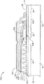
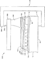
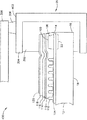
【解決手段】 検出器基板12上に検出器マトリクス104を形成し、該検出器基板12上に該出器マトリクスを取り囲むダム106を形成し、検出器マトリクス上にシンチレータ材料110を形成し、シンチレータ材料上へ少なくとも1つがダムの表面に延び、且つダムを過ぎて延びる密閉カバー118を形成する。
【選択図】 図2
Description
ジタルデータの作成において次第に普及している。幾つかの既知のデジタルX線イメージングシステムにおいて、線源からの放射線は、医学的診断用途で患者などの被検体に向かって配向される。放射線の一部は患者を透過して検出器に衝突し、そこで検出器が放射線を光フォトンに変換して該光フォトンが感知される。検出器は離散的画素、すなわちピクセルのマトリクスに分割され、各ピクセル領域に衝突する放射線の質又は強度に基いて出力信号をコード化する。放射線強度は放射線が患者を透過すると変化するので、出力信号に基づいて再構築された画像は、従来のX線用感光性フィルム技術により利用可能な画像像と同様の患者の組織投影を提供する。
12 検出器ベース面
16 側壁
18 裏面
20 有効検出器領域
22 ダム領域
24 接触フィンガー領域
28 接触フィンガー
100 密閉シール構造
102 接着領域
104 検出器マトリクス
106 ダム
108 厚さ
109 第2の面
110 シンチレータ材料
111 針構造
112 封入コーティング
114 反射層
116 薄膜マスク
118 密閉層
120 腐食保護層
Claims (10)
- 検出器基板12を備え、該基板が検出器ベース面14と、該検出器ベース面から垂直に延びる複数の側壁16とを含むX線検出器パネル組立体10を製造する方法であって、
前記検出器基板上に検出器マトリクス20を形成し、
前記検出器マトリクスを取り囲むダム106を前記検出器基板上に形成し、
前記検出器マトリクス上にシンチレータ材料110を形成し、
少なくとも1つが前記ダムの表面に延び且つ該ダムを過ぎて延びる密閉カバー118を前記シンチレータ材料上に形成する、
段階を含む方法。 - 前記密閉カバーを形成する段階が、
前記シンチレータ材料上に前記ダムを過ぎて延びる封入コーティング112を形成し、
前記封入コーティング上に前記ダムを過ぎて延びる反射層114を形成し、
前記反射層上に前記ダムを過ぎて延びる薄膜マスク116を形成する、
ことをさらに含む請求項1に記載の方法。 - 前記密閉カバーを形成する段階が、
前記ダムを過ぎて延び、且つ前記薄膜マスクを過ぎて延びる密閉層を前記薄膜マスク上に形成し、
前記ダムを過ぎて延び、且つ前記密閉層を過ぎて延びる腐食保護層120を前記密閉層上に形成する、
ことをさらに含む請求項1に記載の方法。 - 前記検出器ベース面14が胸壁側面26を含み、前記密閉カバーを形成する段階が、
前記ダムを過ぎて延び、且つ前記胸壁側面に隣接して少なくとも1つの側壁上に延びる密閉層を前記薄膜マスク上に形成し、
前記ダムを過ぎて延び、且つ前記胸壁側面に隣接して少なくとも1つの側壁上に延びる腐食保護層を前記密閉層上に形成する、
ことをさらに含む請求項3に記載の方法。 - 前記検出器ベース面が反対側にある裏面18と胸壁側面とを含み、前記密閉カバーを形成する段階が、
薄膜マスク上に前記ダムを過ぎて延びる密閉層を形成し、
前記密閉層上に前記ダムを過ぎて延びる腐食保護層を形成し、
末端チャネル304を少なくとも1つの側壁に接続する、
ことを含む請求項3に記載の方法。 - 前記末端チャネルを接続する段階が、前記末端チャネルを前記胸壁側面に接続することを含む請求項5に記載の方法。
- 前記密閉層と前記末端チャネルの間に空隙があるように前記密閉層と前記末端チャネル間に機械カバー308を結合することをさらに含む請求項6に記載の方法。
- 前記密閉カバーを形成する段階が、
前記シンチレータ材料上に前記ダム表面に延びる第1の封入層542を形成し、
前記第1の封入層上に前記検出器マトリクスと前記ダム表面の間の領域まで延びる反射層546を形成し、
前記反射層上に前記ダムの表面上の第1の封入層の端部まで延びる第2の封入層548を形成する、
ことをさらに含む請求項1に記載の方法。 - 検出器基板12と、
前記検出器基板上に形成された検出器マトリクス20と、
前記検出器基板上に形成され、前記検出器マトリクスを取り囲むダム106と、
前記検出器マトリクス上に形成されたシンチレータ材料110と、
前記シンチレータ材料上に形成された密閉カバー118と、
を備え、
前記密閉カバーの端部の少なくとも1つが、前記検出器マトリクスと前記ダムとを過ぎて延び、且つ該検出器マトリクスを過ぎて前記ダム上に延びることを特徴とするデジタルX線パネル10。 - 前記密閉カバーが、
前記シンチレータ材料上で前記ダムを過ぎて延びる封入層112と、
前記封入層上で前記ダムを過ぎて延びる反射層114と、
前記反射層上で前記ダムを過ぎて延びる薄膜マスク116と、
を備える請求項9に記載のデジタルX線パネル。
Applications Claiming Priority (1)
| Application Number | Priority Date | Filing Date | Title |
|---|---|---|---|
| US10/365,093 US7473903B2 (en) | 2003-02-12 | 2003-02-12 | Method and apparatus for deposited hermetic cover for digital X-ray panel |
Publications (3)
| Publication Number | Publication Date |
|---|---|
| JP2004245833A true JP2004245833A (ja) | 2004-09-02 |
| JP2004245833A5 JP2004245833A5 (ja) | 2007-03-22 |
| JP4445281B2 JP4445281B2 (ja) | 2010-04-07 |
Family
ID=32736392
Family Applications (1)
| Application Number | Title | Priority Date | Filing Date |
|---|---|---|---|
| JP2004033028A Expired - Fee Related JP4445281B2 (ja) | 2003-02-12 | 2004-02-10 | X線検出器パネル組立体を製造する方法及びデジタルx線パネル |
Country Status (4)
| Country | Link |
|---|---|
| US (1) | US7473903B2 (ja) |
| JP (1) | JP4445281B2 (ja) |
| DE (1) | DE102004005883A1 (ja) |
| FR (1) | FR2851051A1 (ja) |
Families Citing this family (20)
| Publication number | Priority date | Publication date | Assignee | Title |
|---|---|---|---|---|
| US7492019B2 (en) * | 2003-03-07 | 2009-02-17 | Ic Mechanics, Inc. | Micromachined assembly with a multi-layer cap defining a cavity |
| DE102005055176A1 (de) * | 2005-11-18 | 2007-05-31 | Siemens Ag | Flachbilddetektor |
| JP2007149842A (ja) * | 2005-11-25 | 2007-06-14 | Sanyo Electric Co Ltd | 半導体装置 |
| DE102006022138A1 (de) * | 2006-05-11 | 2007-11-15 | Siemens Ag | Szintillatorplatte |
| DE102006024893A1 (de) * | 2006-05-24 | 2007-12-06 | Siemens Ag | Szintillatorplatte |
| DE102006038969B4 (de) * | 2006-08-21 | 2013-02-28 | Siemens Aktiengesellschaft | Röntgenkonverterelement und Verfahren zu dessen Herstellung |
| JP5883556B2 (ja) * | 2010-06-04 | 2016-03-15 | 浜松ホトニクス株式会社 | 放射線イメージセンサ |
| JP2012168128A (ja) * | 2011-02-16 | 2012-09-06 | Canon Inc | 放射線検出装置及び放射線撮像システム |
| US8415628B1 (en) | 2011-10-31 | 2013-04-09 | General Electric Company | Hermetically sealed radiation detector and methods for making |
| WO2014187502A1 (en) * | 2013-05-24 | 2014-11-27 | Teledyne Dalsa B.V. | A moisture protection structure for a device and a fabrication method thereof |
| US10712454B2 (en) * | 2014-07-25 | 2020-07-14 | General Electric Company | X-ray detectors supported on a substrate having a metal barrier |
| CA2968415C (en) * | 2014-11-21 | 2020-10-27 | Anton Petrus Maria Van Arendonk | Mammography detector with small chest distance |
| JP6487263B2 (ja) * | 2015-04-20 | 2019-03-20 | 浜松ホトニクス株式会社 | 放射線検出器及びその製造方法 |
| US10299744B2 (en) | 2016-11-17 | 2019-05-28 | General Electric Company | Scintillator sealing for solid state x-ray detector |
| US10631801B2 (en) | 2016-11-17 | 2020-04-28 | General Electric Company | Scintillator sealing for solid state X-ray detector |
| US9871073B1 (en) | 2016-11-22 | 2018-01-16 | General Electric Company | Scintillator sealing for solid state X-ray detector |
| US9812510B1 (en) | 2016-12-14 | 2017-11-07 | General Electric Company | Packaging organic photodetectors |
| JP6877289B2 (ja) * | 2017-07-31 | 2021-05-26 | キヤノン株式会社 | 放射線検出装置、放射線検出システム、及び放射線出装置の製造方法 |
| KR102666048B1 (ko) * | 2019-05-29 | 2024-05-13 | 엘지디스플레이 주식회사 | 디지털 엑스레이 검출기와 이를 포함하는 디지털 엑스레이 검출 장치 및 이의 제조 방법 |
| CN114639689B (zh) * | 2020-12-15 | 2025-03-18 | 京东方科技集团股份有限公司 | 平板探测器、其制作方法及x射线成像系统 |
Family Cites Families (19)
| Publication number | Priority date | Publication date | Assignee | Title |
|---|---|---|---|---|
| US5187369A (en) * | 1990-10-01 | 1993-02-16 | General Electric Company | High sensitivity, high resolution, solid state x-ray imaging device with barrier layer |
| US5179284A (en) * | 1991-08-21 | 1993-01-12 | General Electric Company | Solid state radiation imager having a reflective and protective coating |
| US5231654A (en) * | 1991-12-06 | 1993-07-27 | General Electric Company | Radiation imager collimator |
| US5231655A (en) * | 1991-12-06 | 1993-07-27 | General Electric Company | X-ray collimator |
| US5463225A (en) * | 1992-06-01 | 1995-10-31 | General Electric Company | Solid state radiation imager with high integrity barrier layer and method of fabricating |
| US5399884A (en) * | 1993-11-10 | 1995-03-21 | General Electric Company | Radiation imager with single passivation dielectric for transistor and diode |
| US5435608A (en) * | 1994-06-17 | 1995-07-25 | General Electric Company | Radiation imager with common passivation dielectric for gate electrode and photosensor |
| US5430298A (en) * | 1994-06-21 | 1995-07-04 | General Electric Company | CT array with improved photosensor linearity and reduced crosstalk |
| US5517031A (en) * | 1994-06-21 | 1996-05-14 | General Electric Company | Solid state imager with opaque layer |
| US6037609A (en) * | 1997-01-17 | 2000-03-14 | General Electric Company | Corrosion resistant imager |
| US6167110A (en) * | 1997-11-03 | 2000-12-26 | General Electric Company | High voltage x-ray and conventional radiography imaging apparatus and method |
| KR20010043630A (ko) * | 1998-05-15 | 2001-05-25 | 더 보드 오브 트러스티스 오브 더 리랜드 스탠포드 쥬니어 유니버시티 | 치매의 치료를 위한 글루코코티코이드 수용체 길항제 |
| US6172371B1 (en) * | 1998-06-15 | 2001-01-09 | General Electric Company | Robust cover plate for radiation imager |
| US6414315B1 (en) * | 1999-10-04 | 2002-07-02 | General Electric Company | Radiation imaging with continuous polymer layer for scintillator |
| US6396046B1 (en) | 1999-11-02 | 2002-05-28 | General Electric Company | Imager with reduced FET photoresponse and high integrity contact via |
| US6350990B1 (en) * | 1999-11-04 | 2002-02-26 | General Electric Company | End cap and sealing method for imager |
| US6353654B1 (en) * | 1999-12-30 | 2002-03-05 | General Electric Company | Method and apparatus for compensating for image retention in an amorphous silicon imaging detector |
| JP4234304B2 (ja) * | 2000-05-19 | 2009-03-04 | 浜松ホトニクス株式会社 | 放射線検出器 |
| US6642524B2 (en) * | 2002-01-09 | 2003-11-04 | Ge Medical Systems Global Technology Company, Llc | Scintillator sealing for solid state X-ray detector |
-
2003
- 2003-02-12 US US10/365,093 patent/US7473903B2/en not_active Expired - Fee Related
-
2004
- 2004-02-05 DE DE102004005883A patent/DE102004005883A1/de not_active Withdrawn
- 2004-02-10 JP JP2004033028A patent/JP4445281B2/ja not_active Expired - Fee Related
- 2004-02-11 FR FR0401326A patent/FR2851051A1/fr not_active Withdrawn
Also Published As
| Publication number | Publication date |
|---|---|
| JP4445281B2 (ja) | 2010-04-07 |
| FR2851051A1 (fr) | 2004-08-13 |
| US20040155320A1 (en) | 2004-08-12 |
| US7473903B2 (en) | 2009-01-06 |
| DE102004005883A1 (de) | 2004-08-26 |
Similar Documents
| Publication | Publication Date | Title |
|---|---|---|
| JP4445281B2 (ja) | X線検出器パネル組立体を製造する方法及びデジタルx線パネル | |
| JP3077941B2 (ja) | 放射線検出素子及びその製造方法 | |
| CN100397096C (zh) | 放射线检测元件及其制造方法 | |
| JP4317921B2 (ja) | X線検出器アセンブリ | |
| JP2000284053A (ja) | 放射線検出素子 | |
| US20110147602A1 (en) | Radiographic imaging apparatus, radiographic imaging system, and method of producing radiographic imaging apparatus | |
| JPH05242841A (ja) | 防湿シール構造を有する平面x線イメージャ | |
| KR20010052994A (ko) | 방사선 이미지 센서 | |
| TWI591368B (zh) | Radiation detector and manufacturing method thereof | |
| EP1300693B1 (en) | Radiation detector and method of producing the same | |
| JP4099206B2 (ja) | シンチレータパネル及び放射線イメージセンサ | |
| WO2014199925A1 (ja) | 放射線検出器及びその製造方法 | |
| WO2001075478A1 (en) | Radiation detector and method of manufacture thereof | |
| JP3987438B2 (ja) | シンチレータパネル及び放射線イメージセンサ | |
| EP1300694B1 (en) | Radiation detector and method of manufacture thereof | |
| US7053381B2 (en) | Dual para-xylylene layers for an X-ray detector | |
| JP2004301516A (ja) | 放射線検出装置 | |
| JP4283863B2 (ja) | シンチレータパネル | |
| JPS60142300A (ja) | 螢光板及び放射線検出素子 | |
| CN114114373B (zh) | 闪烁体面板及其制作方法、放射线图像检测装置 | |
| JP2001330676A (ja) | 放射線検出器 | |
| EP4325255A1 (en) | Manufacturing method of a radiation imaging apparatus | |
| JP2007205935A (ja) | 放射線検出器 |
Legal Events
| Date | Code | Title | Description |
|---|---|---|---|
| A521 | Request for written amendment filed |
Free format text: JAPANESE INTERMEDIATE CODE: A523 Effective date: 20070206 |
|
| A621 | Written request for application examination |
Free format text: JAPANESE INTERMEDIATE CODE: A621 Effective date: 20070206 |
|
| A131 | Notification of reasons for refusal |
Free format text: JAPANESE INTERMEDIATE CODE: A131 Effective date: 20081202 |
|
| A601 | Written request for extension of time |
Free format text: JAPANESE INTERMEDIATE CODE: A601 Effective date: 20090224 |
|
| A602 | Written permission of extension of time |
Free format text: JAPANESE INTERMEDIATE CODE: A602 Effective date: 20090227 |
|
| A521 | Request for written amendment filed |
Free format text: JAPANESE INTERMEDIATE CODE: A523 Effective date: 20090402 |
|
| RD02 | Notification of acceptance of power of attorney |
Free format text: JAPANESE INTERMEDIATE CODE: A7422 Effective date: 20090402 |
|
| RD04 | Notification of resignation of power of attorney |
Free format text: JAPANESE INTERMEDIATE CODE: A7424 Effective date: 20090402 |
|
| A02 | Decision of refusal |
Free format text: JAPANESE INTERMEDIATE CODE: A02 Effective date: 20090512 |
|
| A521 | Request for written amendment filed |
Free format text: JAPANESE INTERMEDIATE CODE: A523 Effective date: 20090810 |
|
| A911 | Transfer to examiner for re-examination before appeal (zenchi) |
Free format text: JAPANESE INTERMEDIATE CODE: A911 Effective date: 20090928 |
|
| TRDD | Decision of grant or rejection written | ||
| A01 | Written decision to grant a patent or to grant a registration (utility model) |
Free format text: JAPANESE INTERMEDIATE CODE: A01 Effective date: 20091222 |
|
| A01 | Written decision to grant a patent or to grant a registration (utility model) |
Free format text: JAPANESE INTERMEDIATE CODE: A01 |
|
| A61 | First payment of annual fees (during grant procedure) |
Free format text: JAPANESE INTERMEDIATE CODE: A61 Effective date: 20100115 |
|
| R150 | Certificate of patent or registration of utility model |
Free format text: JAPANESE INTERMEDIATE CODE: R150 |
|
| FPAY | Renewal fee payment (event date is renewal date of database) |
Free format text: PAYMENT UNTIL: 20130122 Year of fee payment: 3 |
|
| R250 | Receipt of annual fees |
Free format text: JAPANESE INTERMEDIATE CODE: R250 |
|
| LAPS | Cancellation because of no payment of annual fees |