JP2004260176A - テープおよびその製造方法 - Google Patents
テープおよびその製造方法 Download PDFInfo
- Publication number
- JP2004260176A JP2004260176A JP2004045563A JP2004045563A JP2004260176A JP 2004260176 A JP2004260176 A JP 2004260176A JP 2004045563 A JP2004045563 A JP 2004045563A JP 2004045563 A JP2004045563 A JP 2004045563A JP 2004260176 A JP2004260176 A JP 2004260176A
- Authority
- JP
- Japan
- Prior art keywords
- tape
- conductive layer
- substrate
- conductive
- piezoelectric element
- Prior art date
- Legal status (The legal status is an assumption and is not a legal conclusion. Google has not performed a legal analysis and makes no representation as to the accuracy of the status listed.)
- Granted
Links
- 238000004519 manufacturing process Methods 0.000 title claims abstract description 16
- 239000000758 substrate Substances 0.000 claims description 122
- 239000000463 material Substances 0.000 claims description 37
- 238000000151 deposition Methods 0.000 claims description 14
- 229920000642 polymer Polymers 0.000 claims description 14
- 238000001465 metallisation Methods 0.000 claims description 12
- 239000000919 ceramic Substances 0.000 claims description 11
- 229910010293 ceramic material Inorganic materials 0.000 claims description 9
- 230000005290 antiferromagnetic effect Effects 0.000 claims description 6
- 238000009826 distribution Methods 0.000 claims description 3
- 238000005137 deposition process Methods 0.000 claims description 2
- 238000000034 method Methods 0.000 abstract description 44
- 238000010586 diagram Methods 0.000 abstract description 15
- 239000010410 layer Substances 0.000 description 71
- 229910052751 metal Inorganic materials 0.000 description 46
- 239000002184 metal Substances 0.000 description 46
- 230000008018 melting Effects 0.000 description 33
- 238000002844 melting Methods 0.000 description 33
- 239000004593 Epoxy Substances 0.000 description 25
- KDLHZDBZIXYQEI-UHFFFAOYSA-N Palladium Chemical compound [Pd] KDLHZDBZIXYQEI-UHFFFAOYSA-N 0.000 description 15
- 239000010409 thin film Substances 0.000 description 15
- 238000005304 joining Methods 0.000 description 12
- 239000000945 filler Substances 0.000 description 11
- 239000011521 glass Substances 0.000 description 9
- 239000011888 foil Substances 0.000 description 8
- 238000005498 polishing Methods 0.000 description 8
- 230000008021 deposition Effects 0.000 description 7
- 238000013461 design Methods 0.000 description 7
- 239000010408 film Substances 0.000 description 7
- 239000007791 liquid phase Substances 0.000 description 7
- 230000001052 transient effect Effects 0.000 description 7
- 239000004020 conductor Substances 0.000 description 6
- HFGPZNIAWCZYJU-UHFFFAOYSA-N lead zirconate titanate Chemical compound [O-2].[O-2].[O-2].[O-2].[O-2].[Ti+4].[Zr+4].[Pb+2] HFGPZNIAWCZYJU-UHFFFAOYSA-N 0.000 description 6
- 229910052451 lead zirconate titanate Inorganic materials 0.000 description 6
- 230000005855 radiation Effects 0.000 description 6
- 229910045601 alloy Inorganic materials 0.000 description 5
- 239000000956 alloy Substances 0.000 description 5
- 239000010931 gold Substances 0.000 description 5
- 239000010949 copper Substances 0.000 description 4
- 229910000765 intermetallic Inorganic materials 0.000 description 4
- 229910052763 palladium Inorganic materials 0.000 description 4
- 239000011248 coating agent Substances 0.000 description 3
- 238000000576 coating method Methods 0.000 description 3
- 229910052802 copper Inorganic materials 0.000 description 3
- 229910052737 gold Inorganic materials 0.000 description 3
- 229910052738 indium Inorganic materials 0.000 description 3
- 238000002834 transmittance Methods 0.000 description 3
- CSCPPACGZOOCGX-UHFFFAOYSA-N Acetone Chemical compound CC(C)=O CSCPPACGZOOCGX-UHFFFAOYSA-N 0.000 description 2
- 239000002885 antiferromagnetic material Substances 0.000 description 2
- 238000003491 array Methods 0.000 description 2
- 150000001875 compounds Chemical class 0.000 description 2
- 238000001514 detection method Methods 0.000 description 2
- NKZSPGSOXYXWQA-UHFFFAOYSA-N dioxido(oxo)titanium;lead(2+) Chemical compound [Pb+2].[O-][Ti]([O-])=O NKZSPGSOXYXWQA-UHFFFAOYSA-N 0.000 description 2
- APFVFJFRJDLVQX-UHFFFAOYSA-N indium atom Chemical compound [In] APFVFJFRJDLVQX-UHFFFAOYSA-N 0.000 description 2
- 238000003780 insertion Methods 0.000 description 2
- 230000037431 insertion Effects 0.000 description 2
- 238000007689 inspection Methods 0.000 description 2
- 239000011810 insulating material Substances 0.000 description 2
- 150000002739 metals Chemical class 0.000 description 2
- 239000000203 mixture Substances 0.000 description 2
- 238000012986 modification Methods 0.000 description 2
- 230000004048 modification Effects 0.000 description 2
- 238000007650 screen-printing Methods 0.000 description 2
- 229910052709 silver Inorganic materials 0.000 description 2
- 239000002344 surface layer Substances 0.000 description 2
- 230000003746 surface roughness Effects 0.000 description 2
- 229910052718 tin Inorganic materials 0.000 description 2
- 238000012546 transfer Methods 0.000 description 2
- 229920002799 BoPET Polymers 0.000 description 1
- RYGMFSIKBFXOCR-UHFFFAOYSA-N Copper Chemical compound [Cu] RYGMFSIKBFXOCR-UHFFFAOYSA-N 0.000 description 1
- WHXSMMKQMYFTQS-UHFFFAOYSA-N Lithium Chemical compound [Li] WHXSMMKQMYFTQS-UHFFFAOYSA-N 0.000 description 1
- 239000005041 Mylar™ Substances 0.000 description 1
- BQCADISMDOOEFD-UHFFFAOYSA-N Silver Chemical compound [Ag] BQCADISMDOOEFD-UHFFFAOYSA-N 0.000 description 1
- 239000004809 Teflon Substances 0.000 description 1
- 229920006362 Teflon® Polymers 0.000 description 1
- ATJFFYVFTNAWJD-UHFFFAOYSA-N Tin Chemical compound [Sn] ATJFFYVFTNAWJD-UHFFFAOYSA-N 0.000 description 1
- FKSZLDCMQZJMFN-UHFFFAOYSA-N [Mg].[Pb] Chemical compound [Mg].[Pb] FKSZLDCMQZJMFN-UHFFFAOYSA-N 0.000 description 1
- 238000010521 absorption reaction Methods 0.000 description 1
- NIXOWILDQLNWCW-UHFFFAOYSA-N acrylic acid group Chemical group C(C=C)(=O)O NIXOWILDQLNWCW-UHFFFAOYSA-N 0.000 description 1
- 239000000443 aerosol Substances 0.000 description 1
- 230000004075 alteration Effects 0.000 description 1
- PNEYBMLMFCGWSK-UHFFFAOYSA-N aluminium oxide Inorganic materials [O-2].[O-2].[O-2].[Al+3].[Al+3] PNEYBMLMFCGWSK-UHFFFAOYSA-N 0.000 description 1
- 230000005540 biological transmission Effects 0.000 description 1
- 230000015572 biosynthetic process Effects 0.000 description 1
- 239000000969 carrier Substances 0.000 description 1
- 238000004140 cleaning Methods 0.000 description 1
- 239000002131 composite material Substances 0.000 description 1
- PMHQVHHXPFUNSP-UHFFFAOYSA-M copper(1+);methylsulfanylmethane;bromide Chemical compound Br[Cu].CSC PMHQVHHXPFUNSP-UHFFFAOYSA-M 0.000 description 1
- 239000013078 crystal Substances 0.000 description 1
- 238000005520 cutting process Methods 0.000 description 1
- 230000000694 effects Effects 0.000 description 1
- 239000000835 fiber Substances 0.000 description 1
- PCHJSUWPFVWCPO-UHFFFAOYSA-N gold Chemical compound [Au] PCHJSUWPFVWCPO-UHFFFAOYSA-N 0.000 description 1
- 238000010438 heat treatment Methods 0.000 description 1
- 238000009413 insulation Methods 0.000 description 1
- 150000002500 ions Chemical class 0.000 description 1
- 229910052744 lithium Inorganic materials 0.000 description 1
- FUJCRWPEOMXPAD-UHFFFAOYSA-N lithium oxide Chemical compound [Li+].[Li+].[O-2] FUJCRWPEOMXPAD-UHFFFAOYSA-N 0.000 description 1
- 229910001947 lithium oxide Inorganic materials 0.000 description 1
- CPLXHLVBOLITMK-UHFFFAOYSA-N magnesium oxide Inorganic materials [Mg]=O CPLXHLVBOLITMK-UHFFFAOYSA-N 0.000 description 1
- 239000000395 magnesium oxide Substances 0.000 description 1
- AXZKOIWUVFPNLO-UHFFFAOYSA-N magnesium;oxygen(2-) Chemical compound [O-2].[Mg+2] AXZKOIWUVFPNLO-UHFFFAOYSA-N 0.000 description 1
- 238000013017 mechanical damping Methods 0.000 description 1
- 230000007935 neutral effect Effects 0.000 description 1
- 229910052758 niobium Inorganic materials 0.000 description 1
- 239000010955 niobium Substances 0.000 description 1
- GUCVJGMIXFAOAE-UHFFFAOYSA-N niobium atom Chemical compound [Nb] GUCVJGMIXFAOAE-UHFFFAOYSA-N 0.000 description 1
- 239000002245 particle Substances 0.000 description 1
- 239000012071 phase Substances 0.000 description 1
- 238000007639 printing Methods 0.000 description 1
- 229910052594 sapphire Inorganic materials 0.000 description 1
- 239000010980 sapphire Substances 0.000 description 1
- 230000035945 sensitivity Effects 0.000 description 1
- 239000004332 silver Substances 0.000 description 1
- 239000010944 silver (metal) Substances 0.000 description 1
- 238000005245 sintering Methods 0.000 description 1
- 239000006104 solid solution Substances 0.000 description 1
- VEALVRVVWBQVSL-UHFFFAOYSA-N strontium titanate Chemical compound [Sr+2].[O-][Ti]([O-])=O VEALVRVVWBQVSL-UHFFFAOYSA-N 0.000 description 1
- 238000012360 testing method Methods 0.000 description 1
Images


Classifications
-
- G—PHYSICS
- G01—MEASURING; TESTING
- G01N—INVESTIGATING OR ANALYSING MATERIALS BY DETERMINING THEIR CHEMICAL OR PHYSICAL PROPERTIES
- G01N29/00—Investigating or analysing materials by the use of ultrasonic, sonic or infrasonic waves; Visualisation of the interior of objects by transmitting ultrasonic or sonic waves through the object
- G01N29/22—Details, e.g. general constructional or apparatus details
- G01N29/24—Probes
- G01N29/2437—Piezoelectric probes
- G01N29/245—Ceramic probes, e.g. lead zirconate titanate [PZT] probes
-
- B—PERFORMING OPERATIONS; TRANSPORTING
- B06—GENERATING OR TRANSMITTING MECHANICAL VIBRATIONS IN GENERAL
- B06B—METHODS OR APPARATUS FOR GENERATING OR TRANSMITTING MECHANICAL VIBRATIONS OF INFRASONIC, SONIC, OR ULTRASONIC FREQUENCY, e.g. FOR PERFORMING MECHANICAL WORK IN GENERAL
- B06B1/00—Methods or apparatus for generating mechanical vibrations of infrasonic, sonic, or ultrasonic frequency
- B06B1/02—Methods or apparatus for generating mechanical vibrations of infrasonic, sonic, or ultrasonic frequency making use of electrical energy
- B06B1/06—Methods or apparatus for generating mechanical vibrations of infrasonic, sonic, or ultrasonic frequency making use of electrical energy operating with piezoelectric effect or with electrostriction
- B06B1/0607—Methods or apparatus for generating mechanical vibrations of infrasonic, sonic, or ultrasonic frequency making use of electrical energy operating with piezoelectric effect or with electrostriction using multiple elements
- B06B1/0622—Methods or apparatus for generating mechanical vibrations of infrasonic, sonic, or ultrasonic frequency making use of electrical energy operating with piezoelectric effect or with electrostriction using multiple elements on one surface
-
- G—PHYSICS
- G01—MEASURING; TESTING
- G01L—MEASURING FORCE, STRESS, TORQUE, WORK, MECHANICAL POWER, MECHANICAL EFFICIENCY, OR FLUID PRESSURE
- G01L1/00—Measuring force or stress, in general
- G01L1/16—Measuring force or stress, in general using properties of piezoelectric devices
-
- G—PHYSICS
- G01—MEASURING; TESTING
- G01N—INVESTIGATING OR ANALYSING MATERIALS BY DETERMINING THEIR CHEMICAL OR PHYSICAL PROPERTIES
- G01N29/00—Investigating or analysing materials by the use of ultrasonic, sonic or infrasonic waves; Visualisation of the interior of objects by transmitting ultrasonic or sonic waves through the object
- G01N29/22—Details, e.g. general constructional or apparatus details
- G01N29/24—Probes
- G01N29/2475—Embedded probes, i.e. probes incorporated in objects to be inspected
-
- H—ELECTRICITY
- H10—SEMICONDUCTOR DEVICES; ELECTRIC SOLID-STATE DEVICES NOT OTHERWISE PROVIDED FOR
- H10N—ELECTRIC SOLID-STATE DEVICES NOT OTHERWISE PROVIDED FOR
- H10N30/00—Piezoelectric or electrostrictive devices
- H10N30/01—Manufacture or treatment
- H10N30/07—Forming of piezoelectric or electrostrictive parts or bodies on an electrical element or another base
- H10N30/072—Forming of piezoelectric or electrostrictive parts or bodies on an electrical element or another base by laminating or bonding of piezoelectric or electrostrictive bodies
- H10N30/073—Forming of piezoelectric or electrostrictive parts or bodies on an electrical element or another base by laminating or bonding of piezoelectric or electrostrictive bodies by fusion of metals or by adhesives
-
- H—ELECTRICITY
- H10—SEMICONDUCTOR DEVICES; ELECTRIC SOLID-STATE DEVICES NOT OTHERWISE PROVIDED FOR
- H10N—ELECTRIC SOLID-STATE DEVICES NOT OTHERWISE PROVIDED FOR
- H10N30/00—Piezoelectric or electrostrictive devices
- H10N30/01—Manufacture or treatment
- H10N30/07—Forming of piezoelectric or electrostrictive parts or bodies on an electrical element or another base
- H10N30/074—Forming of piezoelectric or electrostrictive parts or bodies on an electrical element or another base by depositing piezoelectric or electrostrictive layers, e.g. aerosol or screen printing
-
- H—ELECTRICITY
- H10—SEMICONDUCTOR DEVICES; ELECTRIC SOLID-STATE DEVICES NOT OTHERWISE PROVIDED FOR
- H10N—ELECTRIC SOLID-STATE DEVICES NOT OTHERWISE PROVIDED FOR
- H10N39/00—Integrated devices, or assemblies of multiple devices, comprising at least one piezoelectric, electrostrictive or magnetostrictive element covered by groups H10N30/00 – H10N35/00
-
- G—PHYSICS
- G01—MEASURING; TESTING
- G01N—INVESTIGATING OR ANALYSING MATERIALS BY DETERMINING THEIR CHEMICAL OR PHYSICAL PROPERTIES
- G01N2291/00—Indexing codes associated with group G01N29/00
- G01N2291/02—Indexing codes associated with the analysed material
- G01N2291/028—Material parameters
- G01N2291/02827—Elastic parameters, strength or force
-
- G—PHYSICS
- G01—MEASURING; TESTING
- G01N—INVESTIGATING OR ANALYSING MATERIALS BY DETERMINING THEIR CHEMICAL OR PHYSICAL PROPERTIES
- G01N2291/00—Indexing codes associated with group G01N29/00
- G01N2291/26—Scanned objects
- G01N2291/269—Various geometry objects
- G01N2291/2694—Wings or other aircraft parts
Landscapes
- Engineering & Computer Science (AREA)
- Chemical & Material Sciences (AREA)
- General Physics & Mathematics (AREA)
- Physics & Mathematics (AREA)
- General Health & Medical Sciences (AREA)
- Pathology (AREA)
- Analytical Chemistry (AREA)
- Biochemistry (AREA)
- Health & Medical Sciences (AREA)
- Manufacturing & Machinery (AREA)
- Immunology (AREA)
- Life Sciences & Earth Sciences (AREA)
- Mechanical Engineering (AREA)
- Ceramic Engineering (AREA)
- Investigating Or Analyzing Materials By The Use Of Ultrasonic Waves (AREA)
- Transducers For Ultrasonic Waves (AREA)
- Piezo-Electric Or Mechanical Vibrators, Or Delay Or Filter Circuits (AREA)
- Force Measurement Appropriate To Specific Purposes (AREA)
- Testing Or Measuring Of Semiconductors Or The Like (AREA)
Abstract
【解決手段】テープであって、少なくとも部分的に可撓性のある第1の導電層と、少なくとも部分的に可撓性があり、前記第1の導電層に対向して配置される第2の導電層と、前記第1の導電層と前記第2の導電層との間に配置され接合されるセンサ、アクチュエータ、またはトランスデューサのうちの少なくとも1つからなる複数の素子と、前記第1の導電層と前記第2の導電層とに接続し、前記可テープに電力および制御信号を印加する電気接点網とを含む。
【選択図】図1
Description
Claims (8)
- テープであって、
少なくとも部分的に可撓性のある第1の導電層と、
少なくとも部分的に可撓性があり、前記第1の導電層に対向して配置される第2の導電層と、
前記第1の導電層と前記第2の導電層との間に配置され接合されるセンサ、アクチュエータ、またはトランスデューサのうちの少なくとも1つからなる複数の素子と、
前記第1の導電層と前記第2の導電層とに接続し、前記可テープに電力および制御信号を印加する電気接点網とを含むテープ。 - 請求項1に記載のテープにおいて、
前記複数のセンサ、アクチュエータ、またはトランスデューサは、分類されグループとして制御されるテープ。 - 請求項1に記載のテープにおいて、
前記センサ、アクチュエータ、またはトランスデューサのうちの少なくとも1つは、多様な異なる幾何学的形状に形成されるテープ。 - 請求項1に記載のテープにおいて、
前記センサ、アクチュエータ、またはトランスデューサのうちの少なくとも1つは、前記センサ、アクチュエータ、またはトランスデューサの密度が不均一となるように前記テープ上に配置された複数のセンサ、アクチュエータ、またはトランスデューサであるテープ。 - 請求項1に記載のテープにおいて、
前記第1の導電層および前記第2の導電層の少なくともいずれかは、前記センサ、アクチュエータ、またはトランスデューサのうちの少なくとも1つの形状および分布に対応してパターニングしたメタライゼーション層を有するポリマーテープであるテープ。 - 請求項1に記載のテープにおいて、
前記センサ、アクチュエータ、またはトランスデューサの少なくとも1つのうち、ある素子は圧電素子を含む1つの機能セラミック材料から構成され、他の素子は1つ以上の他の機能セラミック材料から構成されるテープ。 - 請求項1に記載のテープにおいて、
前記複数のアクチュエータ、センサ、またはトランスデューサは、堆積工程によって形成した反強磁性、電歪、または磁歪素子構造を含む複数の他の機能セラミック材料であり、
前記反強磁性またはその他の機能セラミック素子構造の第1の表面上に第1の電極が堆積され、前記反強磁性またはその他の機能セラミック素子構造の第2の表面上に第2の電極が堆積されるテープ。 - テープの製造方法であって、
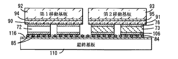
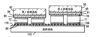
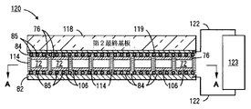
少なくとも1つの第1の基板表面上に材料を堆積して複数の素子構造を形成するステップと、
前記複数の素子構造の各表面上に電極を堆積するステップと、
前記素子構造を第2の基板に接合するステップであって、前記第2の基板は導電性をもつかまたは導電層を有し、かつキャリアプレート上に支持されるステップと、
前記少なくとも1つの第1の基板を前記素子構造から取外すステップと、
第2の側面電極を前記複数の素子構造の第2の表面上に堆積するステップと、
前記素子構造の第2の側面を他の基板に接合するステップであって、前記他の基板は導電性をもつかまたは導電層を有するステップと、
前記キャリアプレートを取外すステップとを含む方法。
Applications Claiming Priority (2)
| Application Number | Priority Date | Filing Date | Title |
|---|---|---|---|
| US10/376,527 | 2003-02-25 | ||
| US10/376,527 US6964201B2 (en) | 2003-02-25 | 2003-02-25 | Large dimension, flexible piezoelectric ceramic tapes |
Publications (2)
| Publication Number | Publication Date |
|---|---|
| JP2004260176A true JP2004260176A (ja) | 2004-09-16 |
| JP4933031B2 JP4933031B2 (ja) | 2012-05-16 |
Family
ID=32771496
Family Applications (1)
| Application Number | Title | Priority Date | Filing Date |
|---|---|---|---|
| JP2004045563A Expired - Fee Related JP4933031B2 (ja) | 2003-02-25 | 2004-02-23 | テープおよびその製造方法 |
Country Status (3)
| Country | Link |
|---|---|
| US (2) | US6964201B2 (ja) |
| EP (3) | EP1808896B1 (ja) |
| JP (1) | JP4933031B2 (ja) |
Cited By (8)
| Publication number | Priority date | Publication date | Assignee | Title |
|---|---|---|---|---|
| JP2008166757A (ja) * | 2006-12-29 | 2008-07-17 | Samsung Electro-Mechanics Co Ltd | 薄膜キャパシタ内蔵型配線基板の製造方法 |
| JP2009232283A (ja) * | 2008-03-24 | 2009-10-08 | Panasonic Electric Works Co Ltd | Baw共振装置の製造方法 |
| US7713366B2 (en) | 2005-10-25 | 2010-05-11 | Ngk Insulators, Ltd. | Piezoelectric/electrostrictive film and method for producing the same |
| JP2011066321A (ja) * | 2009-09-18 | 2011-03-31 | Tdk Corp | 薄膜素子の製造方法及び薄膜素子並びにその薄膜素子を用いたヘッドジンバルアセンブリ、及び、ハードディスクドライブ |
| JP2013161970A (ja) * | 2012-02-06 | 2013-08-19 | Ngk Insulators Ltd | 圧電素子の製造方法 |
| JP2013168654A (ja) * | 2004-12-20 | 2013-08-29 | Palo Alto Research Center Inc | 微細寸法セラミック厚膜素子アレイ、高精細形状セラミック厚膜素子アレイ及び高アスペクト比セラミック厚膜素子アレイの形成方法 |
| JP2015119511A (ja) * | 2013-12-16 | 2015-06-25 | 株式会社デンソー | センサ一体型のイオン伝導性高分子アクチュエータとその製造方法 |
| JP2015534667A (ja) * | 2012-09-04 | 2015-12-03 | ヨアノイム リサーチ フォルシュングスゲゼルシャフト エムベーハーJoanneum Research Forschungsgesellschaft Mbh | 印刷された圧電性圧力検知箔 |
Families Citing this family (86)
| Publication number | Priority date | Publication date | Assignee | Title |
|---|---|---|---|---|
| US7800199B2 (en) * | 2003-06-24 | 2010-09-21 | Oh Choonsik | Semiconductor circuit |
| FR2802340B1 (fr) * | 1999-12-13 | 2003-09-05 | Commissariat Energie Atomique | Structure comportant des cellules photovoltaiques et procede de realisation |
| KR100510821B1 (ko) * | 2003-06-09 | 2005-08-30 | 한국전자통신연구원 | 미세 구조물이 형성된 기판과 그 기판의 제조방법 |
| US7413919B2 (en) * | 2003-06-20 | 2008-08-19 | Acellent Technologies, Inc. | Method of manufacturing a structural health monitoring layer |
| US8071438B2 (en) * | 2003-06-24 | 2011-12-06 | Besang Inc. | Semiconductor circuit |
| US20060207967A1 (en) * | 2003-07-03 | 2006-09-21 | Bocko Peter L | Porous processing carrier for flexible substrates |
| US20050001201A1 (en) * | 2003-07-03 | 2005-01-06 | Bocko Peter L. | Glass product for use in ultra-thin glass display applications |
| WO2005084358A2 (en) * | 2004-03-03 | 2005-09-15 | Metis Design Corporation | Damage detection device |
| US7351608B1 (en) * | 2004-08-19 | 2008-04-01 | The United States Of America As Represented By The Director Of The National Security Agency | Method of precisely aligning components in flexible integrated circuit module |
| JP4078562B2 (ja) * | 2004-08-23 | 2008-04-23 | セイコーエプソン株式会社 | 圧電薄膜共振子の製造方法、圧電薄膜共振子、周波数フィルタ、発振器の製造方法、発振器、電子回路、および電子機器 |
| US7430911B2 (en) * | 2004-08-26 | 2008-10-07 | Acellent Technologies, Inc. | Method of detecting and analyzing changes in the external loading conditions of a structure |
| US7458266B2 (en) * | 2004-09-27 | 2008-12-02 | Samsung Electronics Co. Ltd. | Method and apparatus for detecting a load change upon a structure and analyzing characteristics of resulting damage |
| ES2555683T3 (es) * | 2004-10-07 | 2016-01-07 | Metis Design Corporation | Infraestructura de sensor con electrónica integrada |
| US7070669B1 (en) | 2004-12-20 | 2006-07-04 | Xerox Corporation | Method for forming ceramic thick film element arrays |
| US7488015B2 (en) * | 2004-12-22 | 2009-02-10 | Bayerische Motoren Werke Aktiengesellschaft | Vehicle systems and methods for detecting pedestrian impacts |
| US8030132B2 (en) * | 2005-05-31 | 2011-10-04 | Semiconductor Energy Laboratory Co., Ltd. | Manufacturing method of semiconductor device including peeling step |
| TWI256082B (en) * | 2005-06-01 | 2006-06-01 | Touch Micro System Tech | Method of segmenting a wafer |
| US20070018083A1 (en) * | 2005-06-13 | 2007-01-25 | Acellent Technologies, Inc. | Structural health monitoring layer having distributed electronics |
| US7387033B2 (en) * | 2005-06-17 | 2008-06-17 | Acellent Technologies, Inc. | Single-wire sensor/actuator network for structure health monitoring |
| US8336457B2 (en) * | 2005-06-22 | 2012-12-25 | Nanofoil Corporation | Reactive composite material structures with electrostatic discharge protection and applications thereof |
| US20070069021A1 (en) * | 2005-09-27 | 2007-03-29 | Palo Alto Research Center Incorporated | Smart floor tiles/carpet for tracking movement in retail, industrial and other environments |
| US7596078B2 (en) * | 2005-11-10 | 2009-09-29 | Acellent Technologies, Inc. | Method and apparatus for reducing crosstalk in a structural health monitoring system |
| US7395189B2 (en) | 2005-11-14 | 2008-07-01 | Acellent Technologies, Inc. | Method and apparatus for switching among elements of a structural health monitoring system |
| US7467857B2 (en) * | 2005-12-20 | 2008-12-23 | Palo Alto Research Center Incorporated | Micromachined fluid ejectors using piezoelectric actuation |
| US7533578B2 (en) * | 2006-04-18 | 2009-05-19 | Metis Design Corporation | Triangulation with co-located sensors |
| KR100734403B1 (ko) * | 2006-06-02 | 2007-07-02 | 삼성전기주식회사 | 전자소자 패키지 및 그 제조방법 |
| US7764005B2 (en) | 2006-08-08 | 2010-07-27 | Palo Alto Research Center Incorporated | Traveling wave grids with agitated surface using piezoelectric effect and acoustic traveling waves |
| US20100161283A1 (en) * | 2006-10-03 | 2010-06-24 | Xinlin Qing | Structural health monitoring network |
| US20080155357A1 (en) * | 2006-10-03 | 2008-06-26 | Acellent Technologies, Inc. | Structural health monitoring network |
| US7696676B2 (en) * | 2006-12-18 | 2010-04-13 | Lockheed Martin Corporation | Piezoelectric composite apparatus and related methods |
| US9823833B2 (en) * | 2007-06-05 | 2017-11-21 | Immersion Corporation | Method and apparatus for haptic enabled flexible touch sensitive surface |
| JP5268305B2 (ja) * | 2007-08-24 | 2013-08-21 | 株式会社半導体エネルギー研究所 | 半導体装置の作製方法 |
| US8201325B2 (en) * | 2007-11-22 | 2012-06-19 | International Business Machines Corporation | Method for producing an integrated device |
| US8209857B2 (en) * | 2009-06-19 | 2012-07-03 | The Regents Of The University Of Michigan | Method of making a thin film device |
| DE102010005403A1 (de) * | 2010-01-22 | 2011-07-28 | Epcos Ag, 81669 | Verfahren zur Herstellung eines piezoelektrischen Vielschichtbauelements und piezoelektrisches Vielschichtbauelement |
| JP5399970B2 (ja) * | 2010-03-31 | 2014-01-29 | パナソニック株式会社 | 強誘電体デバイスの製造方法 |
| CN101844130A (zh) * | 2010-05-14 | 2010-09-29 | 中国科学技术大学 | 阵列式硅微超声换能器及其制造方法 |
| JP5463510B2 (ja) * | 2010-06-22 | 2014-04-09 | 独立行政法人科学技術振興機構 | 物理量センサ及びその製造方法 |
| JP5814764B2 (ja) * | 2010-12-27 | 2015-11-17 | キヤノン株式会社 | 記録素子基板、記録ヘッド、および記録ヘッドの製造方法 |
| EP2489442A1 (en) | 2011-02-18 | 2012-08-22 | Aernnova Engineering Solutions Iberica | Integrated phased array transducer, system and methodology for structural health monitoring of aerospace structures |
| US10238166B2 (en) | 2011-06-28 | 2019-03-26 | Robert Rosenbaum | Instrumented article of fitness and method of determining caloric requirements |
| US10543662B2 (en) | 2012-02-08 | 2020-01-28 | Corning Incorporated | Device modified substrate article and methods for making |
| US10014177B2 (en) | 2012-12-13 | 2018-07-03 | Corning Incorporated | Methods for processing electronic devices |
| US10086584B2 (en) | 2012-12-13 | 2018-10-02 | Corning Incorporated | Glass articles and methods for controlled bonding of glass sheets with carriers |
| TWI617437B (zh) | 2012-12-13 | 2018-03-11 | 康寧公司 | 促進控制薄片與載體間接合之處理 |
| US9340443B2 (en) | 2012-12-13 | 2016-05-17 | Corning Incorporated | Bulk annealing of glass sheets |
| FR3000213B1 (fr) * | 2012-12-21 | 2015-05-15 | Eads Europ Aeronautic Defence | Dispositif reconfigurable de controle d'une structure composite par ultrasons |
| US9939900B2 (en) | 2013-04-26 | 2018-04-10 | Immersion Corporation | System and method for a haptically-enabled deformable surface |
| WO2014176528A1 (en) | 2013-04-26 | 2014-10-30 | Immersion Corporation | Passive stiffness and active deformation haptic output devices for flexible displays |
| US9033227B2 (en) * | 2013-05-20 | 2015-05-19 | Ncr Corporation | Methods and systems for performing security weight checks at checkouts |
| US10510576B2 (en) | 2013-10-14 | 2019-12-17 | Corning Incorporated | Carrier-bonding methods and articles for semiconductor and interposer processing |
| US10046542B2 (en) | 2014-01-27 | 2018-08-14 | Corning Incorporated | Articles and methods for controlled bonding of thin sheets with carriers |
| CN106457758B (zh) | 2014-04-09 | 2018-11-16 | 康宁股份有限公司 | 装置改性的基材制品及其制备方法 |
| JP6079931B2 (ja) * | 2014-04-18 | 2017-02-15 | 株式会社村田製作所 | 押圧センサ |
| US9690381B2 (en) | 2014-08-21 | 2017-06-27 | Immersion Corporation | Systems and methods for shape input and output for a haptically-enabled deformable surface |
| US9535550B2 (en) | 2014-11-25 | 2017-01-03 | Immersion Corporation | Systems and methods for deformation-based haptic effects |
| JP2018524201A (ja) | 2015-05-19 | 2018-08-30 | コーニング インコーポレイテッド | シートをキャリアと結合するための物品および方法 |
| US11905201B2 (en) | 2015-06-26 | 2024-02-20 | Corning Incorporated | Methods and articles including a sheet and a carrier |
| US10985078B2 (en) * | 2015-11-06 | 2021-04-20 | Lam Research Corporation | Sensor and adjuster for a consumable |
| FR3044168A1 (fr) * | 2015-11-20 | 2017-05-26 | Crystal Device Tech | Generateur a base de materiau piezoelectrique massif en structure souple |
| US10770646B2 (en) | 2016-03-01 | 2020-09-08 | Qualcomm Incorporated | Manufacturing method for flexible PMUT array |
| TW202216444A (zh) | 2016-08-30 | 2022-05-01 | 美商康寧公司 | 用於片材接合的矽氧烷電漿聚合物 |
| TWI810161B (zh) | 2016-08-31 | 2023-08-01 | 美商康寧公司 | 具以可控制式黏結的薄片之製品及製作其之方法 |
| GB2557894B (en) * | 2016-10-01 | 2019-12-11 | Peratech Holdco Ltd | Flexible sensor |
| US10680161B1 (en) | 2017-03-29 | 2020-06-09 | Apple Inc. | Electronic Devices with Piezoelectric Ink |
| CN106875850A (zh) * | 2017-04-18 | 2017-06-20 | 京东方科技集团股份有限公司 | 一种柔性显示屏及其变形驱动方法、显示装置 |
| CN111372772A (zh) | 2017-08-18 | 2020-07-03 | 康宁股份有限公司 | 使用聚阳离子聚合物的临时结合 |
| US11331692B2 (en) | 2017-12-15 | 2022-05-17 | Corning Incorporated | Methods for treating a substrate and method for making articles comprising bonded sheets |
| US10440848B2 (en) | 2017-12-20 | 2019-10-08 | Immersion Corporation | Conformable display with linear actuator |
| CN108039405B (zh) * | 2018-01-11 | 2023-10-20 | 中国工程物理研究院总体工程研究所 | 一种压电元件、压电传感器和速度及位移检测装置 |
| US11638353B2 (en) * | 2018-09-17 | 2023-04-25 | Hutchinson Technology Incorporated | Apparatus and method for forming sensors with integrated electrical circuits on a substrate |
| WO2020078541A1 (de) * | 2018-10-16 | 2020-04-23 | Fraunhofer-Gesellschaft zur Förderung der angewandten Forschung e.V. | Biegewandler als aktor, biegewandler als sensor, biegewandlersystem |
| CN110196125B (zh) * | 2019-04-19 | 2020-11-06 | 浙江大学 | 一种基于多孔结构的岛桥式柔性传感阵列装置 |
| US11061064B2 (en) * | 2019-05-15 | 2021-07-13 | Nanya Technology Corporation | Semiconductor device and method for detecting cracks |
| CN110265544A (zh) * | 2019-06-24 | 2019-09-20 | 京东方科技集团股份有限公司 | 压电传感器及制备方法、进行指纹识别的方法及电子设备 |
| US11231397B2 (en) * | 2019-07-26 | 2022-01-25 | The Boeing Company | Remote wide bandwidth ultrasonic inspection method and apparatus |
| JP7186685B2 (ja) * | 2019-09-20 | 2022-12-09 | 株式会社ジャパンディスプレイ | 圧力センサ |
| CN111053298B (zh) * | 2019-12-20 | 2022-03-15 | 深圳麦克韦尔科技有限公司 | 柔性发热体及其制造方法和柔性发热组件及气溶胶产生器 |
| FR3118178B1 (fr) * | 2020-12-23 | 2023-07-21 | Buerkert Werke Gmbh & Co Kg | Moyen de mesure de fluide |
| CN113267289B (zh) * | 2021-04-16 | 2022-08-16 | 上海交通大学 | 面向航空发动机的阵列式柔性压电传感器及其制备方法 |
| CN113877792B (zh) * | 2021-09-27 | 2023-01-13 | 北京信息科技大学 | 基于液态金属的大面积柔性压电换能器及其表面导电处理方法 |
| US12313478B2 (en) * | 2021-10-01 | 2025-05-27 | Sensitronics, LLC | Low drift force sensor with capacitive capability |
| CN114112405B (zh) * | 2021-11-23 | 2023-06-20 | 上海交通大学 | 一种用于航空发动机的多模态力学传感器及制备方法 |
| CN116454107A (zh) * | 2022-01-05 | 2023-07-18 | 重庆康佳光电技术研究院有限公司 | 显示背板、显示背板组件、显示装置、检测装置及方法 |
| JP2024000195A (ja) * | 2022-06-20 | 2024-01-05 | キオクシア株式会社 | 半導体装置の製造方法 |
| FR3144487A1 (fr) * | 2022-12-23 | 2024-06-28 | Commissariat À L’Energie Atomique Et Aux Energies Alternatives | Dispositif piézoélectrique |
Citations (9)
| Publication number | Priority date | Publication date | Assignee | Title |
|---|---|---|---|---|
| JPS6151884A (ja) * | 1984-08-22 | 1986-03-14 | Hitachi Ltd | 感圧素子 |
| JPH10125931A (ja) * | 1996-08-27 | 1998-05-15 | Seiko Epson Corp | 薄膜素子の転写方法,薄膜素子,薄膜集積回路装置,アクティブマトリクス基板および液晶表示装置 |
| JPH10249768A (ja) * | 1997-03-12 | 1998-09-22 | Tokai Rubber Ind Ltd | 力センサー |
| WO2000051190A1 (en) * | 1999-02-26 | 2000-08-31 | Active Control Experts, Inc. | Packaged strain actuator |
| JP2000275123A (ja) * | 1999-03-25 | 2000-10-06 | Tokai Rubber Ind Ltd | 分布センサ |
| JP2000337979A (ja) * | 1999-05-27 | 2000-12-08 | Tokai Rubber Ind Ltd | 分布センサ |
| US6335263B1 (en) * | 2000-03-22 | 2002-01-01 | The Regents Of The University Of California | Method of forming a low temperature metal bond for use in the transfer of bulk and thin film materials |
| JP2002102392A (ja) * | 2000-08-01 | 2002-04-09 | Head Sport Ag | 球技スポーツ用ラケットおよびその製造方法 |
| JP2003019176A (ja) * | 2001-07-07 | 2003-01-21 | Hirohide Miwa | 人体用広面積超音波照射子 |
Family Cites Families (29)
| Publication number | Priority date | Publication date | Assignee | Title |
|---|---|---|---|---|
| JPS5492307A (en) | 1977-12-29 | 1979-07-21 | Sony Corp | Driving circuit of electrostrictive converter |
| US4233477A (en) * | 1979-01-31 | 1980-11-11 | The United States Of America As Represented By The Secretary Of The Navy | Flexible, shapeable, composite acoustic transducer |
| US4670682A (en) | 1984-12-21 | 1987-06-02 | General Electric Company | Piezoelectric ceramic switching devices and systems and method of making the same |
| JPS63150979A (ja) | 1986-12-16 | 1988-06-23 | Toshiba Corp | 電気回路しや断器 |
| US4906840A (en) * | 1988-01-27 | 1990-03-06 | The Board Of Trustees Of Leland Stanford Jr., University | Integrated scanning tunneling microscope |
| JPH025325A (ja) | 1988-06-10 | 1990-01-10 | Fuji Electric Co Ltd | 圧電リレー |
| JP2794720B2 (ja) * | 1988-08-23 | 1998-09-10 | 松下電器産業株式会社 | 複合圧電振動子 |
| JPH02162782A (ja) | 1988-12-15 | 1990-06-22 | Murata Mfg Co Ltd | バイモルフ型変位素子の駆動方法 |
| EP0408306B1 (en) | 1989-07-11 | 1996-05-01 | Ngk Insulators, Ltd. | Piezoelectric/electrostrictive actuator having at least one piezoelectric/electrostrictive film |
| US4991283A (en) * | 1989-11-27 | 1991-02-12 | Johnson Gary W | Sensor elements in multilayer ceramic tape structures |
| JPH0423370A (ja) | 1990-05-15 | 1992-01-27 | Ube Ind Ltd | バイモルフ素子 |
| DE69223096T2 (de) | 1991-07-18 | 1998-05-28 | Ngk Insulators Ltd | Piezoelektrischer/elektrostriktiver Element mit einem keramischen Substrat aus stabilisiertem Zirkoniumdioxid |
| US5869189A (en) * | 1994-04-19 | 1999-02-09 | Massachusetts Institute Of Technology | Composites for structural control |
| US5486494A (en) * | 1994-07-22 | 1996-01-23 | Texas Instruments Incorporated | Method and apparatus for affixing spheres to a conductive sheet |
| US5585136A (en) | 1995-03-22 | 1996-12-17 | Queen's University At Kingston | Method for producing thick ceramic films by a sol gel coating process |
| US5691960A (en) * | 1995-08-02 | 1997-11-25 | Materials Systems, Inc. | Conformal composite acoustic transducer panel and method of fabrication thereof |
| EP1758169A3 (en) * | 1996-08-27 | 2007-05-23 | Seiko Epson Corporation | Exfoliating method, transferring method of thin film device, and thin film device, thin film integrated circuit device, and liquid crystal display device produced by the same |
| EP0907212A1 (en) | 1996-11-29 | 1999-04-07 | Ngk Insulators, Ltd. | Ceramic element, method of manufacturing ceramic element, display, relay device, and capacitor |
| JP3200026B2 (ja) * | 1997-04-04 | 2001-08-20 | 日本碍子株式会社 | 周設センサ |
| WO1999000252A1 (en) * | 1997-06-27 | 1999-01-07 | Seiko Epson Corporation | Piezoelectric vibrator unit, method for manufacturing the same, and ink-jet recording head |
| JPH1126834A (ja) | 1997-07-04 | 1999-01-29 | Toshio Fukuda | Pzt薄膜バイモルフ形の平行平板構造体、及びその製造方法 |
| US6071795A (en) | 1998-01-23 | 2000-06-06 | The Regents Of The University Of California | Separation of thin films from transparent substrates by selective optical processing |
| DK1066119T3 (da) * | 1998-03-26 | 2005-04-04 | Exogen Inc | Paneler fremstillet af fleksible transducerelementer |
| US6370964B1 (en) * | 1998-11-23 | 2002-04-16 | The Board Of Trustees Of The Leland Stanford Junior University | Diagnostic layer and methods for detecting structural integrity of composite and metallic materials |
| US6715192B2 (en) | 1998-12-28 | 2004-04-06 | Ngk Insulators, Ltd. | Method for manufacturing a piezoelectric/electrostrictive device |
| JP2000332313A (ja) | 1999-05-21 | 2000-11-30 | Matsushita Electric Ind Co Ltd | 薄膜圧電型バイモルフ素子及びその応用 |
| JP2001274528A (ja) * | 2000-01-21 | 2001-10-05 | Fujitsu Ltd | 薄膜デバイスの基板間転写方法 |
| JP4387623B2 (ja) * | 2000-12-04 | 2009-12-16 | キヤノン株式会社 | 圧電素子の製造方法 |
| US6771007B2 (en) * | 2002-04-17 | 2004-08-03 | The Boeing Company | Vibration induced perpetual energy resource |
-
2003
- 2003-02-25 US US10/376,527 patent/US6964201B2/en not_active Expired - Fee Related
-
2004
- 2004-02-23 JP JP2004045563A patent/JP4933031B2/ja not_active Expired - Fee Related
- 2004-02-25 EP EP07007909.0A patent/EP1808896B1/en not_active Expired - Lifetime
- 2004-02-25 EP EP04004266.5A patent/EP1453103B1/en not_active Expired - Lifetime
- 2004-02-25 EP EP10179398A patent/EP2270865A3/en not_active Withdrawn
- 2004-12-20 US US11/017,470 patent/US7118990B1/en not_active Expired - Fee Related
Patent Citations (10)
| Publication number | Priority date | Publication date | Assignee | Title |
|---|---|---|---|---|
| JPS6151884A (ja) * | 1984-08-22 | 1986-03-14 | Hitachi Ltd | 感圧素子 |
| JPH10125931A (ja) * | 1996-08-27 | 1998-05-15 | Seiko Epson Corp | 薄膜素子の転写方法,薄膜素子,薄膜集積回路装置,アクティブマトリクス基板および液晶表示装置 |
| JPH10249768A (ja) * | 1997-03-12 | 1998-09-22 | Tokai Rubber Ind Ltd | 力センサー |
| WO2000051190A1 (en) * | 1999-02-26 | 2000-08-31 | Active Control Experts, Inc. | Packaged strain actuator |
| JP2003527046A (ja) * | 1999-02-26 | 2003-09-09 | アクティブ コントロール エキスパーツ,インコーポレイテッド | パッケージングされたひずみアクチュエータ |
| JP2000275123A (ja) * | 1999-03-25 | 2000-10-06 | Tokai Rubber Ind Ltd | 分布センサ |
| JP2000337979A (ja) * | 1999-05-27 | 2000-12-08 | Tokai Rubber Ind Ltd | 分布センサ |
| US6335263B1 (en) * | 2000-03-22 | 2002-01-01 | The Regents Of The University Of California | Method of forming a low temperature metal bond for use in the transfer of bulk and thin film materials |
| JP2002102392A (ja) * | 2000-08-01 | 2002-04-09 | Head Sport Ag | 球技スポーツ用ラケットおよびその製造方法 |
| JP2003019176A (ja) * | 2001-07-07 | 2003-01-21 | Hirohide Miwa | 人体用広面積超音波照射子 |
Cited By (9)
| Publication number | Priority date | Publication date | Assignee | Title |
|---|---|---|---|---|
| JP2013168654A (ja) * | 2004-12-20 | 2013-08-29 | Palo Alto Research Center Inc | 微細寸法セラミック厚膜素子アレイ、高精細形状セラミック厚膜素子アレイ及び高アスペクト比セラミック厚膜素子アレイの形成方法 |
| US7713366B2 (en) | 2005-10-25 | 2010-05-11 | Ngk Insulators, Ltd. | Piezoelectric/electrostrictive film and method for producing the same |
| JP2008166757A (ja) * | 2006-12-29 | 2008-07-17 | Samsung Electro-Mechanics Co Ltd | 薄膜キャパシタ内蔵型配線基板の製造方法 |
| US7845073B2 (en) | 2006-12-29 | 2010-12-07 | Samsung Electro-Mechanics Co., Ltd. | Method of manufacturing circuit board embedding thin film capacitor |
| JP2009232283A (ja) * | 2008-03-24 | 2009-10-08 | Panasonic Electric Works Co Ltd | Baw共振装置の製造方法 |
| JP2011066321A (ja) * | 2009-09-18 | 2011-03-31 | Tdk Corp | 薄膜素子の製造方法及び薄膜素子並びにその薄膜素子を用いたヘッドジンバルアセンブリ、及び、ハードディスクドライブ |
| JP2013161970A (ja) * | 2012-02-06 | 2013-08-19 | Ngk Insulators Ltd | 圧電素子の製造方法 |
| JP2015534667A (ja) * | 2012-09-04 | 2015-12-03 | ヨアノイム リサーチ フォルシュングスゲゼルシャフト エムベーハーJoanneum Research Forschungsgesellschaft Mbh | 印刷された圧電性圧力検知箔 |
| JP2015119511A (ja) * | 2013-12-16 | 2015-06-25 | 株式会社デンソー | センサ一体型のイオン伝導性高分子アクチュエータとその製造方法 |
Also Published As
| Publication number | Publication date |
|---|---|
| US6964201B2 (en) | 2005-11-15 |
| EP1453103A3 (en) | 2006-04-12 |
| EP1808896A1 (en) | 2007-07-18 |
| EP1453103B1 (en) | 2013-09-04 |
| EP2270865A2 (en) | 2011-01-05 |
| US20060211217A1 (en) | 2006-09-21 |
| EP1808896B1 (en) | 2017-04-12 |
| JP4933031B2 (ja) | 2012-05-16 |
| EP1453103A2 (en) | 2004-09-01 |
| US20040163478A1 (en) | 2004-08-26 |
| US7118990B1 (en) | 2006-10-10 |
| EP2270865A3 (en) | 2012-04-18 |
Similar Documents
| Publication | Publication Date | Title |
|---|---|---|
| JP4933031B2 (ja) | テープおよびその製造方法 | |
| US7234214B2 (en) | Methods for making thick film elements | |
| KR100508222B1 (ko) | 공통접지전극을구비한복합소자음향프로브 | |
| JP4362996B2 (ja) | 格子状配列構造の圧電/電歪アクチュエータ及びその製造方法 | |
| JP4151420B2 (ja) | デバイスの製造方法 | |
| US7290336B2 (en) | Method of fabricating an array of multi-electroded piezoelectric transducers for piezoelectric diaphragm structures | |
| CN113826235A (zh) | 用于制造具有承载基底的显示器的方法、根据该方法制造的承载基底和确定用于柔性的显示器的覆盖玻璃 | |
| US20030102777A1 (en) | Ultrasonic transducer and method of manufacturing the same | |
| JP6478902B2 (ja) | 貫通配線基板の製造方法、及び電子デバイスの製造方法 | |
| US8551863B2 (en) | Method for manufacturing ferroelectric device | |
| KR20160018393A (ko) | 전극이 관통 배선과 접속된 디바이스, 및 그 제조 방법 | |
| CN110085127B (zh) | 柔性显示母板及柔性显示屏制作方法 | |
| JP2003526903A (ja) | 差動型pztアクチベータの電極パターンの形成 | |
| JP2001509901A (ja) | 音響プローブの製造方法 | |
| JPH1032454A (ja) | マイクロ圧電振動子 | |
| CN109534284B (zh) | 用于微电极与柔性排线之间热压焊接的方法 | |
| JP6021463B2 (ja) | 液体吐出ヘッド、および液体吐出ヘッドの製造方法 | |
| US20040049901A1 (en) | Method for making a multielement acoustic probe using a metallised and ablated polymer as ground plane | |
| JP2006245094A (ja) | 薄膜圧電体素子の製造方法および薄膜圧電体素子の転写方法 | |
| US20060232171A1 (en) | Piezoelectric diaphragm assembly with conductors on flexible film | |
| JPH03173652A (ja) | 圧電素子の貼着方法 | |
| CN114284424A (zh) | 一种压电器件、压电设备及其制作方法 | |
| JP3377922B2 (ja) | 積層型圧電アクチュエータ | |
| KR101873640B1 (ko) | 플렉서블 소자 패키징 방법 및 이에 의하여 제조된 플렉서블 소자 | |
| JP2010232456A (ja) | 圧電体素子の製造方法及び圧電体素子 |
Legal Events
| Date | Code | Title | Description |
|---|---|---|---|
| A621 | Written request for application examination |
Free format text: JAPANESE INTERMEDIATE CODE: A621 Effective date: 20070216 |
|
| A977 | Report on retrieval |
Free format text: JAPANESE INTERMEDIATE CODE: A971007 Effective date: 20101126 |
|
| A131 | Notification of reasons for refusal |
Free format text: JAPANESE INTERMEDIATE CODE: A131 Effective date: 20101207 |
|
| A601 | Written request for extension of time |
Free format text: JAPANESE INTERMEDIATE CODE: A601 Effective date: 20110307 |
|
| A602 | Written permission of extension of time |
Free format text: JAPANESE INTERMEDIATE CODE: A602 Effective date: 20110310 |
|
| A601 | Written request for extension of time |
Free format text: JAPANESE INTERMEDIATE CODE: A601 Effective date: 20110405 |
|
| A602 | Written permission of extension of time |
Free format text: JAPANESE INTERMEDIATE CODE: A602 Effective date: 20110408 |
|
| A601 | Written request for extension of time |
Free format text: JAPANESE INTERMEDIATE CODE: A601 Effective date: 20110427 |
|
| A602 | Written permission of extension of time |
Free format text: JAPANESE INTERMEDIATE CODE: A602 Effective date: 20110506 |
|
| A521 | Request for written amendment filed |
Free format text: JAPANESE INTERMEDIATE CODE: A523 Effective date: 20110602 |
|
| TRDD | Decision of grant or rejection written | ||
| A01 | Written decision to grant a patent or to grant a registration (utility model) |
Free format text: JAPANESE INTERMEDIATE CODE: A01 Effective date: 20120124 |
|
| A01 | Written decision to grant a patent or to grant a registration (utility model) |
Free format text: JAPANESE INTERMEDIATE CODE: A01 |
|
| A61 | First payment of annual fees (during grant procedure) |
Free format text: JAPANESE INTERMEDIATE CODE: A61 Effective date: 20120216 |
|
| R150 | Certificate of patent or registration of utility model |
Free format text: JAPANESE INTERMEDIATE CODE: R150 |
|
| FPAY | Renewal fee payment (event date is renewal date of database) |
Free format text: PAYMENT UNTIL: 20150224 Year of fee payment: 3 |
|
| R250 | Receipt of annual fees |
Free format text: JAPANESE INTERMEDIATE CODE: R250 |
|
| R250 | Receipt of annual fees |
Free format text: JAPANESE INTERMEDIATE CODE: R250 |
|
| R250 | Receipt of annual fees |
Free format text: JAPANESE INTERMEDIATE CODE: R250 |
|
| LAPS | Cancellation because of no payment of annual fees |